 | –≠–ª–µ–∫—Ç—Ä–æ–Ω–Ω—ã–π –∫–æ–º–ø–æ–Ω–µ–Ω—Ç: LA75503V | –°–∫–∞—á–∞—Ç—å:  PDF PDF  ZIP ZIP |
Ordering number : ENN6804
41301RM (OT) No. 6804-1/15
Overview
The LA75503V is an adjustment free VIF/SIF signal
processing IC for PAL TV/VCR.
It supports 38 MHz, 38.9 MHz, and 39.5 MHz as the IF
frequencies, as well as PAL sound multi-system (M/N,
B/G, I, D/K), and contains an on-chip sound carrier trap
and sound carrier BPF. To adjust the VCO circuit, AFT
circuit, and sound filter, 4-MHz external crystal or 4-MHz
external signal is needed.
Functions
∑ VIF amplifier
∑ VCO adjustment free PLL detection circuit
∑ Digital AFT circuit
∑ RF AGC
∑ Buzz canceller
∑ Equalizer amplifier
∑ Internal sound carrier BPF
∑ Internal sound carrier trap
∑ PLL-FM detector
∑ Reference oscillation circuit
Features
∑ Internal VCO adjustment free circuit eliminating need
for VCO coil adjustments.
∑ Internal sound carrier BPF and sound carrier trap enable
easy configuration of PAL sound multi-system at low
cost.
∑ Considerably reduces the number of required peripheral
parts.
∑ Use of digital AFT eliminates problem of AFT
tolerance.
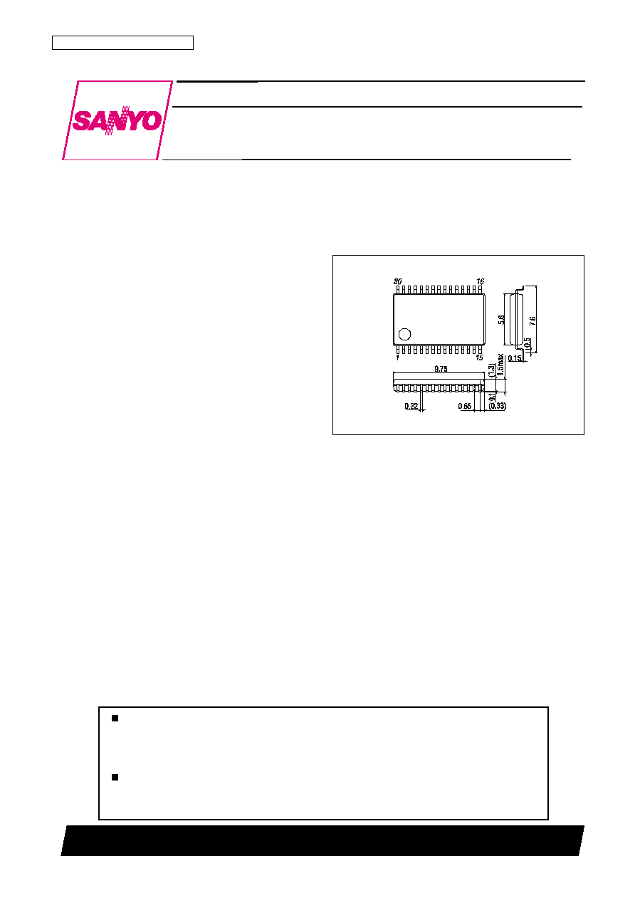
∑ Package: SSOP30 (275 mil)
Package Dimensions
unit: mm
3191A-SSOP30 (275 mil)
SANYO: SSOP30 (275 mil)
[LA75503V]
LA75503V
SANYO Electric Co.,Ltd. Semiconductor Company
TOKYO OFFICE Tokyo Bldg., 1-10, 1 Chome, Ueno, Taito-ku, TOKYO, 110-8534 JAPAN
Adjustment Free VIF/SIF Signal Processing IC
for PAL TV/VCR
Monolithic Linear IC
Any and all SANYO products described or contained herein do not have specifications that can handle
applications that require extremely high levels of reliability, such as life-support systems, aircraft's
control systems, or other applications whose failure can be reasonably expected to result in serious
physical and/or material damage. Consult with your SANYO representative nearest you before using
any SANYO products described or contained herein in such applications.
SANYO assumes no responsibility for equipment failures that result from using products at values that
exceed, even momentarily, rated values (such as maximum ratings, operating condition ranges, or other
parameters) listed in products specifications of any and all SANYO products described or contained
herein.
No. 6804-2/15
LA75503V
Parameter
Symbol
Conditions
Ratings
Unit
Maximum supply voltage
V
CC
max
7
V
Circuit voltage
V16
V
CC
V
V18
V
CC
V
I30
≠1
mA
Circuit current
I17
+0.5
mA
I6
≠10
mA
I4
≠3
mA
Allowable power dissipation
Pd max
Ta
70∞C (
*
Mounted on a printed circuit board)
550
mW
Operating temperature
Topr
≠20 to +70
∞C
Storage temperature
Tstg
≠55 to +150
∞C
Specifications
Maximum Ratings
at Ta = 25∞C
Parameter
Symbol
Conditions
Ratings
Unit
Recommended supply voltage
V
CC
5
V
Operating voltage range
V
CC
op
4.5 to 5.5
V
Operating Conditions
at Ta = 25∞C
Parameter
Symbol
Conditions
Ratings
Unit
min
typ
max
[VIF Block ]
Circuit current
I17
64.0
73.6
mA
Maximum RF AGC voltage
V14H
Collector load 30 k
VC2 = 9 V
8.5
9
--
V
Minimum RF AGC voltage
V14L
0.3
0.7
V
Input sensitivity
Vi
33
39
45
dBµV
AGC range
GR
58
dB
Maximum allowable input
Vimax
92
97
dBµV
No-signal video output voltage
V4
3.3
3.6
3.9
V
Synchronizing signal tip voltage
V4tip
1.0
1.3
1.6
V
Video output level
V
O
1.7
2.0
2.3
Vpp
Video signal-to-noise ratio
S/N
B/G
48
52
dB
C-S beating
IC-S
P/S = 10 dB
26
32
38
dB
Differential gain
DG
Vin = 80 dBµ
3
10
%
Differential phase
DP
2
10
deg
Black noise threshold voltage
VBTH
0.7
V
Black noise clamp voltage
VBCL
1.8
V
VIF input resistance
Ri
2.5
3.0
k
VIF input capacitance
Ci
3
6
PF
Maximum AFT voltage
V13H
4.3
4.7
5.0
V
Minimum AFT voltage
V13L
0
0.2
0.7
V
AFT tolerance 1
dfa1
f = 38.9 MHz
±35
±70
kHz
AFT tolerance 2
dfa2
f = 38.0 MHz
±35
±70
kHz
AFT tolerance 3
dfa3
f = 39.5 MHz
±35
±70
kHz
AFT detection sensitivity
Sf
RL = 100 k
//100 k
40
80
120
mV/kHz
AFT dead zone
fda
30
60
kHz
APC pull-in range (U)
fpu
1.5
2.0
MHz
APC pull-in range (L)
fpl
1.5
2.0
MHz
VCO maximum frequency range (U)
dfu
1.5
2.0
MHz
VCO maximum frequency range (L)
dfl
1.5
2.0
MHz
VCO control sensitivity
2.0
4.0
8.0
kHz/mV
Electrical Characteristics
at Ta = 25∞C, V
CC
= 5.0 V, fp = 38.9 MHz
Note:
*
Circuit board dimensions: 65
◊
72
◊
1.6 mm
3
, material: paper phenol.
Continued on next page.
No. 6804-3/15
LA75503V
Continued from preceding page.
Parameter
Symbol
Conditions
Ratings
Unit
min
typ
max
N trap1 (4.75 MHz)
NT1
wrt 1 MHz
≠30
≠35
dB
N trap2 (5.25 MHz)
NT2
wrt 1 MHz
≠19
≠24
dB
BG trap1 (5.75 MHz)
BT1
wrt 1 MHz
≠27
≠32
dB
BG trap2 (6.1 MHz)
BT2
wrt 1 MHz
≠20
≠25
dB
BG trap3 (5.85 MHz)
BT3
wrt 1 MHz
≠27
≠32
dB
I trap1 (6.25 MHz)
IT1
wrt 1 MHz
≠25
≠30
dB
I trap2 (6.8 MHz)
IT2
wrt 1 MHz
≠15
≠20
dB
DK trap1 (6.75 MHz)
DT1
wrt 1 MHz
≠25
≠30
dB
Group delay 1 NTSC (3.0 MHz)
NGD1
wrt 1 MHz
10
40
70
ns
Group delay 1-1 NTSC (3.5 MHz)
NGD1-1
wrt 1 MHz
70
120
170
ns
Group delay 2 BG (4 MHz)
BGD2
wrt 1 MHz
30
60
90
ns
Group delay 2-1 BG (4.4 MHz)
BGD2-1
wrt 1 MHz
100
150
200
ns
Group delay 3 I (4 MHz)
IGD3
wrt 1 MHz
0
30
60
ns
Group delay 3-1 I (4.4 MHz)
IGD3-1
wrt 1 MHz
30
60
90
ns
Group delay 4 DK (4 MHz)
DGD4
wrt 1 MHz
0
15
30
ns
Group delay 4-1 DK (4.4 MHz)
DGD4-1
wrt 1 MHz
0
30
60
ns
[1st SIF Block]
Conversion gain
Vg
fp = 5.5 MHz, Vi = 500µV
26
32
38
dB
SIF carrier output level
So
Vi = 10 mV
100
mVrms
First SIF maximum input
Simax
So ±2 dB
106
dBµV
First SIF input resistance
Ris
5.0
6.0
k
First SIF input capacitance
Cis
3
6
pF
[SIF Block]
Limiting sensitivity
Vi(lim)
fp = 5.5 MHz,
F = ±30 kHz at 400 Hz
46
52
58
dBµV
FM detector output voltage
Vo(FM)
560
700
850
mVrms
AM rejection ratio
AMR
AM = 30% at 400 Hz
50
60
dB
Total harmonic distortion
THD
f = 5.5 MHz,
F = ±30 kHz
0.3
1.0
%
FM detector output S/N
S/N(FM)
55
60
dB
BPF 3-dB bandwidth
BW
±100
kHz
PAL de-emphasis
Pdeem
fm = 3 kHz
≠3
dB
NTSC de-emphasis
Ndeem
fm = 2 kHz
≠3
dB
PAL/NT audio voltage gain difference
GD
6
dB
[Others]
4-MHz level (during external input)
X4MIN
Terminated
86
dBµ
SIF system SW threshold voltage
V10, V11
1.4
V
IF system SW threshold resistance
V12
270
k
Split/inter SW
V16
0.5
V
System Switching
No. 6804-4/15
LA75503V
∑ SIF system switch
The SIF system is switched by setting pins A (pin 13) and B (pin 14) to GND or OPEN.
A
B
B/G
I
D/K
M/N
FM DET LEVEL
De-emphasis
GND
GND
O
6 dB
75 µs
GND
OPEN
O
0 dB
50 µs
OPEN
GND
O
0 dB
50 µs
OPEN
OPEN
O
0 dB
50 µs
Note: "O" indicates that the system is selected.
∑ IF system switch
38.9 MHz is selected as the IF frequency by leaving pin 15 (crystal oscillation) open. 38 MHz is selected by adding
220 k
between pin 15 and GND. This device can also select 39.5 MHz operation by adding a 220 k
resistor between
pin 15 and V
CC
.
∑ Split/inter carrier switch
Inter carrier is selected by setting the first SIF input (pin 20) to GND.
Sound Trap
The trapping point of the sound trap is set approximately 250 kHz above the SIF center frequency of each mode to
improve the video S/N. Therefore, design using split specifications is preferable.
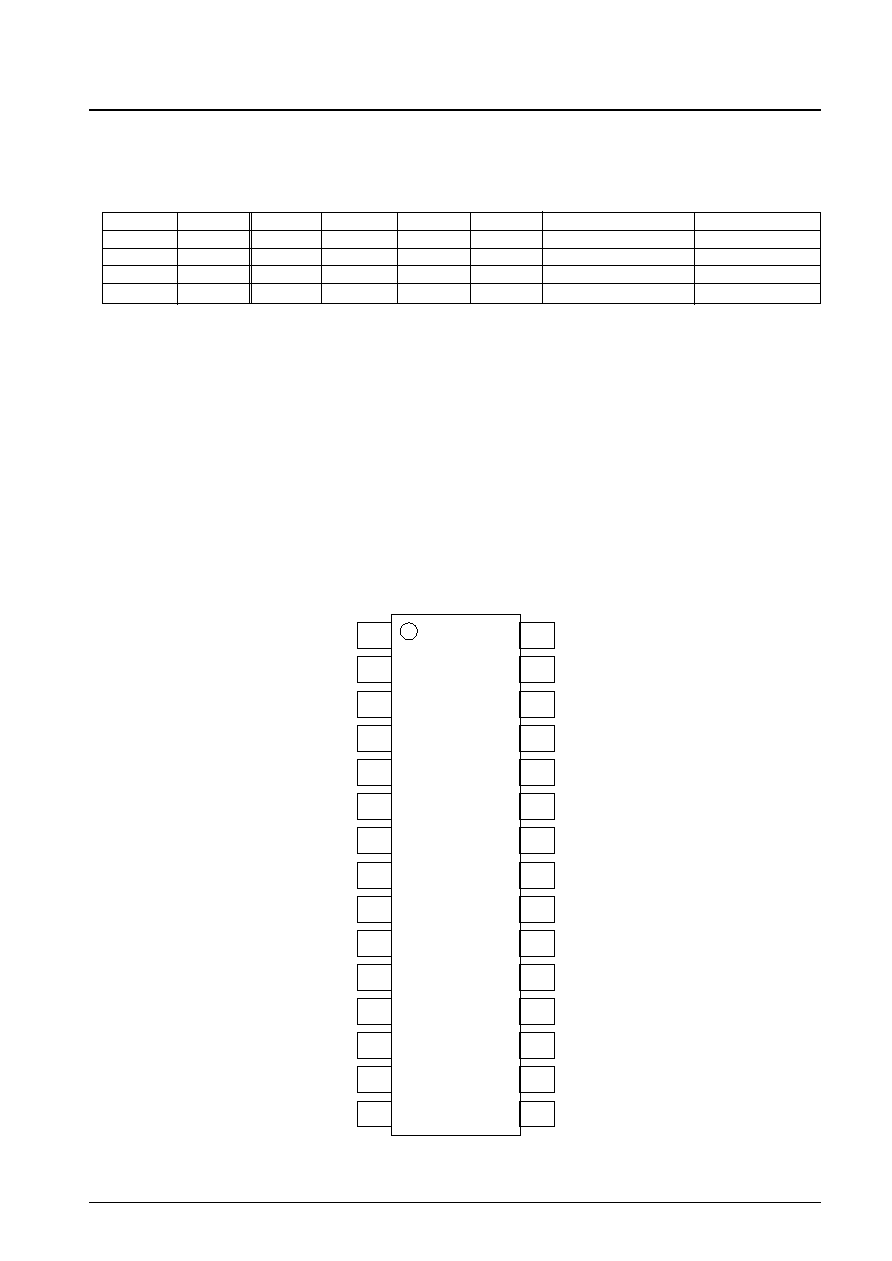
Pin Assignment
25
2
1
SIF INPUT
FM FILTER
NC
1st SIF OUT
NC
VIDEO DET OUT
EQ FILTER
SIF AGC FILTER
APC FILTER
FLL FILTER
VCO COIL
VCO COIL
SYSTEM SW [A]
SYSTEM SW [B]
REF OSC
FM DET OUT
FM NOISE FILTER
RF AGC VR
SIF PLL FILTER
NC
FILTER CONTROL CAPACITOR
VIF INPUT
VIF INPUT
GND
VCC
1st SIF INPUT
NC
IF AGC FILTER
RF AGC OUT
AFT OUT
3
4
5
6
7
8
9
22
23
24
26
27
28
29
30
LA75503V
10
11
12
19
20
21
13
14
15
16
17
18
Top view
No. 6804-5/15
LA75503V
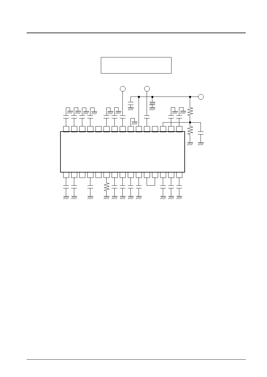
Test Circuit
Input Impedance Measuring Circuit (VIF, First SIF input impedance)
30 29 28 27 26 25 24 23 22 21 20 19 18 17 16
1
2
3
4
5
6
7
8
9
10 11
12 13 14 15
100
µ
F
+
15 k
10 k
1 k
VIF INPUT
Impedance analyzer
*:
0.01
µ
F in case of unspecified capacitor
1st SIF INPUT
VCC
LA75503V
Top view