 | –≠–ª–µ–∫—Ç—Ä–æ–Ω–Ω—ã–π –∫–æ–º–ø–æ–Ω–µ–Ω—Ç: LA7567GM | –°–∫–∞—á–∞—Ç—å:  PDF PDF  ZIP ZIP |

Any and all SANYO products described or contained herein do not have specifications that can handle
applications that require extremely high levels of reliability, such as life-support systems, aircraft's
control systems, or other applications whose failure can be reasonably expected to result in serious
physical and/or material damage. Consult with your SANYO representative nearest you before using
any SANYO products described or contained herein in such applications.
SANYO assumes no responsibility for equipment failures that result from using products at values that
exceed, even momentarily, rated values (such as maximum ratings, operating condition ranges, or other
parameters) listed in products specifications of any and all SANYO products described or contained
herein.
Overview
The LA7567GM is an NTSC SPLIT support VIF/SIF IF
IC that adopts a semi-adjustment-free system. The VIF
block adopts a technique that makes AFT adjustment
unnecessary by adjusting the VCO, thus simplifying the
adjustment steps in the manufacturing process. PLL
detection is adopted in the FM detector. A 5-V power-
supply voltage is used to match that used in most
multimedia systems. In addition, this IC also includes a
buzz canceller to suppress Nyquist buzz and provide high
audio quality.
Functions
[VIF]
∑ VIF amplifier ∑ PLL detector ∑ BNC ∑ RF AGC
∑ EQ amplifier ∑ AFT ∑ IF AGC ∑ Buzz canceller
[First SIF]
∑ First SIF ∑ First SIF detector ∑ AGC
[SIF]
∑ Multi-format SIF converter ∑ Limiter amplifier ∑ PLL
FM detector
Features
∑ Both AFT and SIF inductors built in, thus making
adjustment of external inductance unnecessary.
∑ Built-in buzz canceller for excellent audio performance.
∑ V
CC
= 5 V, low power dissipation (250 mW)
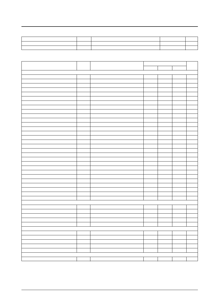
Package Dimensions
unit: mm
3112A-MFP24S
Monolithic Linear IC
D1401RM (OT) No. 6803-1/14
1
12
24
13
12.5
(0.75)
1.0
0.15
0.35
5.4
7.6
0.63
1.7max
1.5
0.1
SANYO: MFP24S
[LA7567GM]
SANYO Electric Co.,Ltd. Semiconductor Company
TOKYO OFFICE Tokyo Bldg., 1-10, 1 Chome, Ueno, Taito-ku, TOKYO, 110-8534 JAPAN
TV and VCR VIF/SIF IF Signal-Processing Circuit with
NTSC SPLIT Support
LA7567GM
Ordering number : ENN6803
Parameter
Symbol
Conditions
Ratings
Unit
Maximum supply voltage
V
CC
max
6
V
Circuit voltage
V13, V17
V
CC
V
I6
≠3
mA
Circuit current
I10
≠10
mA
I24
≠2
mA
Allowable power dissipation
Pd max
TA
50∞C, Independent IC
420
mW
*
: Mounted on a printed circuit board
720
mW
Operating temperature
Topr
≠20 to +70
∞C
Storage temperature
Tstg
≠55 to +150
∞C
Specifications
Maximum Ratings
at Ta = 25∞C
Note: When mounted on a 65
◊
72
◊
1.6 mm paper/phenolic resin printed circuit board.
No. 6803-2/14
LA7567GM
Parameter
Symbol
Conditions
Ratings
Unit
Recommended supply voltage
V
CC
5
V
Operating supply voltage range
V
CC
op
4.5 to 5.5
V
Operating Conditions
at Ta = 25∞C
Parameter
Symbol
Conditions
Ratings
Unit
min
typ
max
[VIF Block]
Circuit current
I5
40
47.5
54.5
mA
Maximum RF AGC voltage
V14H
V
CC
≠ 0.5
V
CC
V
Minimum RF AGC voltage
V14L
0
0.5
V
Input sensitivity
V
IN
S1 = OFF
27
33
39
dBµV
AGC range
G
R
53
58
dB
Maximum allowable input
V
IN
max
90
96
dBµV
No-signal state video output voltage
V6
2.1
2.4
2.7
V
Synchronizing signal tip voltage
V6 tip
0.7
1.0
1.3
V
Video output level
V
O
0.95
1.1
1.25
Vp-p
Black noise threshold voltage
V
BTH
0.5
0.8
1.1
V
Black noise clamp voltage
V
BCL
1.2
1.5
1.8
V
Video signal-to-noise ratio
S/N
48
52
dB
C-S beat
IC-S
38
43
dB
Frequency characteristics
f
C
6 MHz
≠3.0
≠1.5
dB
Differential gain
DG
3.0
6.5
%
Differential phase
DP
3
5
deg
No-signal state AFT voltage
V13
2.0
2.5
3.0
V
Maximum AFT voltage
V13H
4.0
4.4
5.0
V
Minimum AFT voltage
V13L
0
0.18
1.00
V
AFT detection sensitivity
Sf
14
21
28
mV/kHz
VIF input resistance
R
IN
45.75 MHz
1.5
k
VIF input capacitance
C
IN
45.75 MHz
3
pF
APC pull-in range (U)
f
PU
0.7
1.5
MHz
APC pull-in range (L)
f
PL
≠2.0
≠1.4
MHz
AFT tolerance frequency 1
dfa1
≠200
0
+200
kHz
VCO1 maximum variability range (U)
dfu
1.0
1.5
MHz
VCO1 maximum variability range (L)
dfl
≠2.0
≠1.4
MHz
VCO control sensitivity
B
1.2
3.2
5.0
kHz/mV
Sync ratio
VS
25.0
28.5
31.5
%
[First SIF Block]
Conversion gain
VG
27
33
39
dB
4.5 MHz output level
S
O
53
115
180
mVrms
First SIF maximum input
S
IN
max
8
16
mVrms
First SIF input resistance
R
IN
(SIF)
41.25 MHz
2
k
First SIF input capacitance
C
IN
(SIF)
41.25 MHz
3
pF
[SIF Block]
Limiting sensitivity
Vli (lim)
44
50
56
dBµV
FM detector output voltage
V
O
(FM)
4.5 MHz ±25 kHz
*
350
450
570
mVrms
AMR rejection ratio
AMR
50
60
dB
Total harmonic distortion
THD
0.3
0.8
%
SIF S/N
S/N (FM)
59
65
[SIF Converter]
Maximum output level
V max
110
116
122
dBµV
Electrical Characteristics
at Ta = 25∞C, V
CC
= 5.0 V, fp = 45.75 MHz
Note:
*
The FM detector output level can be reduced and the FM dynamic range can be increased by inserting a resistor and a capacitor in series between
pin 23 and ground.
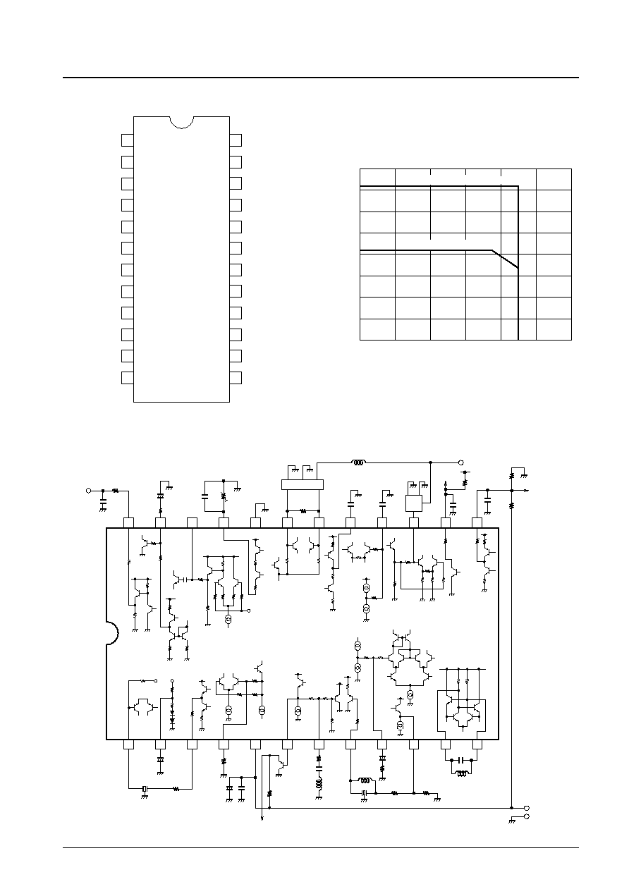
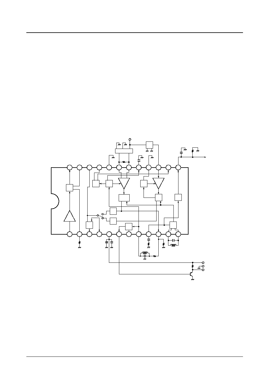
Pin Assignment
Internal Equivalent Circuit and External Components
No. 6803-3/14
LA7567GM
1
2
3
4
5
6
7
8
9
10
11
12
13
14
15
16
17
18
19
20
21
22
23
24
2nd SIF INPUT
BIAS FILTER
MIX OUT
CER.OSC
VCC
VIDEO OUT
EQ FILTER
EQ INPUT
APC FILTER
VIDEO DET OUT
VCO COIL
VCO COIL
AFT OUT
RF AGC OUT
1st SIF INPUT
1st SIF AGC FILTER
IF AGC FILTER
VIF
VIF
GND
RF AGC VR
1st SIF OUT
(NICAM OUT)
FM FILTER
FM DET OUT
A13679
LA7567GM
Top view
SAW(P)
+
+
+
VCO
COIL
100
k
100
k
7.5k
330
150
3k
330
10k
10k
-
B
300
1k
30pF
620
1k
1k
400
400
1k
30k
1k
1k
1k
1k
10k
2k
2k
1k
100
2k
6k
500
3.3k
200
9.2k
1.2k
1.2k
1k
1k
1k
2k
200
10k
18k
SAW
(S)
24
23
22
21
20
19
18
17
16
15
14
13
1
2
3
4
5
6
7
8
9
10
11
12
100
µ
F
0.47
µ
F
0.47 to 1
µ
F
0.01
µ
F
VIDEO
OUT
0.01
µ
F
0.01
µ
F
1
µ
F
0.022
µ
F
0.01
µ
F
0.01
µ
F
0.01
µ
F
AUDIO
OUT PUT
RFAGC
VR
RF AGC
OUT PUT
IF
9V
IN PUT
GND
BPF
AFT
OUTPUT
V
CC
V
V
V
1V
6MHz
T00134
Allowable power dissipation, Pd max -- W
Ambient temperature, Ta -- ∞C
0
80
100
60
70
40
20
-20
0
Pd max -- Ta
200
100
400
300
600
500
800
700
720
420
Independent IC
Mounted on a printed circuit board
AC Characteristics Test Circuit
Test Circuit
No. 6803-4/14
LA7567GM
+
+
+
+
100
k
100
k
30k
100
k
1.5
k
7.5k
330
560
10k
10k
150
51
10k
-
B
51
51
FM
DET
RF
AGC
IF
AGC
AGC
1st
DET
VCO
EQ
AMP
MIX
HPF
HPF
VIDEO
DET
HPF
AFT
LIM
AMP
VIF
AMP
24
23
22
21
20
19
18
17
16
15
14
13
1
2
3
4
5
6
7
8
9
10
11
12
1st
AMP
1
µ
F
0.01
µ
F
0.47
µ
F
0.01
µ
F
1
µ
F
(M
)
(D)
(A)
(E)
0.01
µ
F
0.01
µ
F
0.01
µ
F
0.01
µ
F
0.01
µ
F
0.01
µ
F
0.01
µ
F
0.01
µ
F
1000
pF
24pF
(M
)
(F)
(B)
FM DET OUT
GND
IF AGC
1st SIF IN
2nd SIF IN
CONV.OUT
VIDEO
OUT
VIF IN
RF AGC
9V
OUT
V
CC
GND
AFT
OUT
T00135
RF AGC
V
R
1st SIF OUT
(NICAM OUT)
S
2
S1
+
100
k
100
k
10k
330
10k
24
23
22
21
20
19
18
17
16
15
14
13
1
2
3
4
5
6
7
8
9
10
11
12
100
µ
F
0.01
µ
F
0.01
µ
F
0.01
µ
F
0.01
µ
F
0.01
µ
F
0.01
µ
F
0.01
µ
F
0.01
µ
F
0.01
µ
F
0.01
µ
F
0.01
µ
F
0.01
µ
F
V
CC
T00136
1st SIF IN
VIF IN
Impedance
analyzer
LA7567GM
No. 6803-5/14
LA7567GM
Application Circuit Diagrams
NT (US) SPLIT
+
+
2.2k
100
k
100
k
1k
7.5k
330
560
10k
150
330
10k
-
B
FM
DET
SAW
(S)
RF
AGC
IF
AGC
AGC
1st
DET
VCO
EQ
AMP
MIX
HPF
HPF
VIDEO
DET
SAW(P)
HPF
AFT
LIM
AMP
VIF
AMP
24
23
22
21
20
19
18
17
16
15
14
13
1
2
3
4
5
6
7
8
9
10
11
12
1st
AMP
100
µ
F
1
µ
F
0.01
µ
F
15
µ
H
0.47
µ
F
0.01
µ
F
(M
)
0.022
µ
F
1
µ
H
0.01
µ
F
0.01
µ
F
1000
pF
(M
)
AF OUT
GND
TSF1241
IN PUT
RF AGC
OUT
GND
VIDEO
OUT
BPF
AFT
OUT
V
CC
T00138
+
1
µ
F
30k
9V
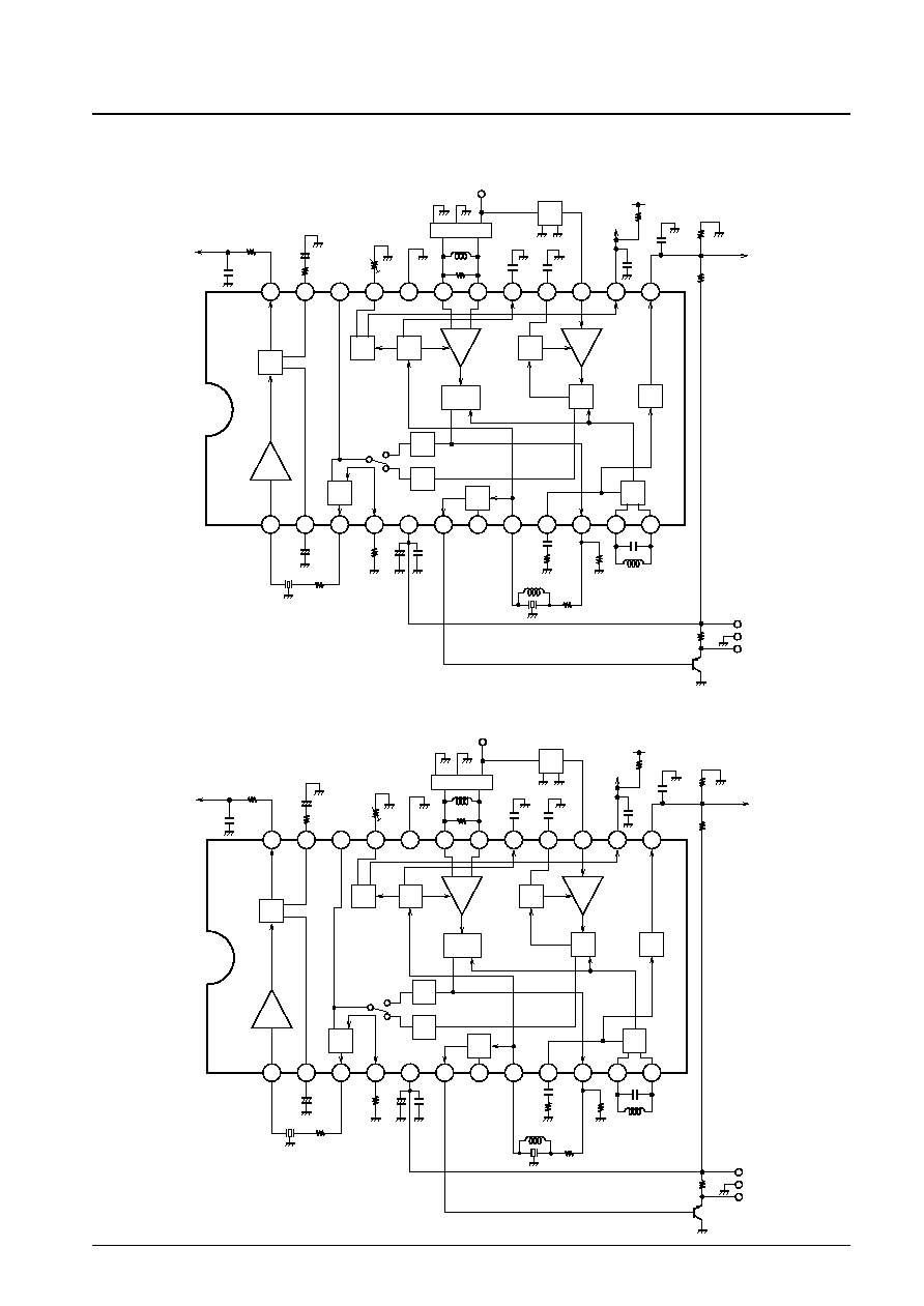
JAPAN SPLIT
+
+
+
1
µ
F
2.2k
100
k
100
k
1k
7.5k
330
560
10k
150
330
10k
-
B
FM
DET
SAW
(S)
RF
AGC
IF
AGC
AGC
1st
DET
VCO
EQ
AMP
MIX
HPF
HPF
VIDEO
DET
SAW(P)
HPF
AFT
LIM
AMP
VIF
AMP
24
23
22
21
20
19
18
17
16
15
14
13
1
2
3
4
5
6
7
8
9
10
11
12
1st
AMP
100
µ
F
1
µ
F
0.01
µ
F
15
µ
H
0.47
µ
F
0.01
µ
F
(M
)
0.022
µ
F
0.01
µ
F
0.01
µ
F
1000
pF
(M
)
AF OUT
GND
TSF1137
IN PUT
RF AGC
OUT
GND
VIDEO
OUT
BPF
AFT
OUT
V
CC
T00139
30k
9V

No. 6803-6/14
LA7567GM
NT (US) INTER
+
+
GND
+
1
µ
F
2.2k
100
k
100
k
7.5k
330
560
100k
150
330
10k
-
B
FM
DET
RF
AGC
IF
AGC
AGC
1st
DET
VCO
EQ
AMP
MIX
HPF
HPF
VIDEO
DET
SAW(P)
HPF
AFT
LIM
AMP
VIF
AMP
24
23
22
21
20
19
18
17
16
15
14
13
1
2
3
4
5
6
7
8
9
10
11
12
1st
AMP
100
µ
F
1
µ
F
0.01
µ
F
15
µ
H
0.47
µ
F
0.01
µ
F
22
µ
H
(M
)
0.022
µ
F
0.01
µ
F
1000
pF
62pF
(M
)
AF OUT
TSF5220
IN PUT
RF AGC
OUT
V
CC
GND
VIDEO
OUT
BPF
AFT
OUT
*
INTER
16PIN
GND
T00140
30k
9V
Sample Application Circuit
When the SIF, first SIF, AFT, and RF AGC circuits are not used:
∑ When the SIF circuit is not used:
Leave pins 1, 23, and 24 open.
Connect pin 2 to ground through a 2-k
resistor.
∑ When the first SIF circuit is not used:
Leave pins 3, 4, 15 and 22 open.
Connect pin 16 to ground.
∑ When the AFT circuit is not used:
Since there is no way to defeat the AFT circuit, connect a 100-k
resistor and a 0.01-µF capacitor in parallel between
pin 13 and ground.
∑ When the RF AGC circuit is not used:
Leave pins 14 and 21 open.
Insert a 0.01-µF capacitor between pin 21 and ground for oscillation prevention.
No. 6803-7/14
LA7567GM
2.2k
100
k
1k
330
560
2k
150
FM
DET
SAW
(S)
RF
AGC
IF
AGC
AGC
1st
DET
VCO
EQ
AMP
MIX
HPF
HPF
VIDEO
DET
SAW(P)
HPF
AFT
LIM
AMP
VIF
AMP
24
23
22
21
20
19
18
17
16
15
14
13
1
2
3
4
5
6
7
8
9
10
11
12
1st
AMP
+
100
µ
F
0.01
µ
F
15
µ
H
0.47
µ
F
(M
)
GND
TSF5315
IN PUT
GND
VIDEO
OUT
AFT
OUT
V
CC
T00141

No. 6803-8/14
LA7567GM
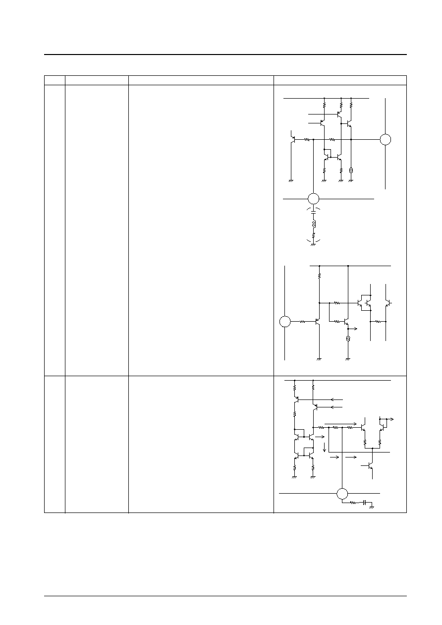
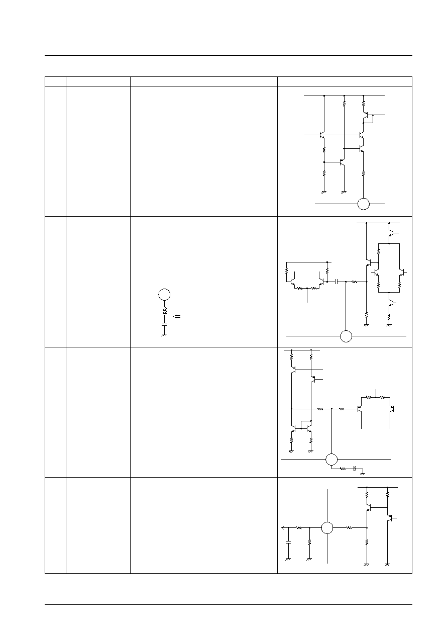
Pin Descriptions
Pin No.
Pin
Description
Equivalent circuit
1
SIF INPUT
∑ SIF input. The input impedance is about 1 k
. Since
buzzing and buzz beating can occur if interference enters
this input pin, care must be taken when design the pattern
layout for this pin. Note that the video and chrominance
signals are especially likely to interfere with the audio
signal. Also, the VIF carrier signal can also cause
interference.
1
1k
1k
A13680
2
FM power supply filter
∑ FM detector bias line filter input. Used to improve the FM
detector signal-to-noise ratio.
C1 should be at least 0.47 µF, and 1 µF is recommended.
If the FM detector is not used, connect pin 2 to ground
through a 2-k
resistor. This stops the FM detector VCO.
2
A13681
C1
3.6V
5k
5k
18k
3
4
SIF converter
∑ Pin 3 is the SIF converter output. The signal is passed
through a 6-MHz bandpass filter and input to the SIF
circuit.
3
4
A13682
A12030
200
10k
400
4(R)
5
V
CC
∑ Use the shortest distance possible when decoupling V
CC
and ground.
Continued on next page.
No. 6803-9/14
LA7567GM
Continued from preceding page.
Pin No.
Pin
Description
Equivalent circuit
6
7
8
EQ amp
∑ Equalizer circuit. This circuit is used to correct the video
signal frequency characteristics.
Pin 8 is the EQ amplifier input. This amplifier amplifies a
1.5-V p-p video signal to 2-V p-p.
∑ Notes on equalizer amplifier design
The equalizer amplifier is designed as a voltage follower
amplifier with a gain of about 0 dB. When used for
frequency characteristics correction, a capacitor, inductor,
and resistor must be connected in series between pin 7
and ground.
∑ Approach used in the equalizer amplifier
If vi is the input signal and vo is the output signal, then:
Where G is the voltage-follower amplifier gain.
Assume:
vin: Imaginary short
G: About 0 dB
vin
0.
Then:
∑ R1 is the IC internal resistance, and is 1 k
. In the
application design, simply select Z to correspond to the
desired characteristics. However, since the EQ amplifier
gain will be maximum at the resonant point defined by Z,
care is required to assure that distortion does not occur.
6
7
8
2k
200
EQ INPUT
EQ OUTPUT
AGC
C
R
L =Z
1k
A13683
A13684
9
APC FILTER
∑ PLL detector APC filter connection. The APC time constant
is switched internally in the IC. When locked, the VCO is
controlled by loop A and the loop gain is reduced. When
unlocked and during weak field reception, the VCO is
controlled by loop B and the loop gain is increased.
For this APC filter we recommend:
R = 150 to 390
C = 0.47 µF
9
1k
1k
1k
A
B
FROM
APC DET
A13685
C
+
R
R1
---- +1 (vi + vin) = Vo
◊
G
2
voG
R1
AV = ---- = ---- +1
vi
Z
Continued on next page.
No. 6803-10/14
LA7567GM
Continued from preceding page.
Pin No.
Pin
Description
Equivalent circuit
10
Composite video output
∑ Output for the video signal that includes the SIF carrier.
A resistor must be inserted between pin 10 and ground to
acquire adequate drive capability.
R
430
10
2k
15pF
2pF
A13686
11
12
VCO tank
∑ VCO tank circuit used for video signal detection.
See the coil specifications provided separately for details
on the tank circuit. This VCO is a vector synthesis VCO.
11
12
A13687
13
AFT OUTPUT
∑ AFT output. The AFT center voltage is generated by an
external bleeder resistor. The AFT gain is increased by
increasing the resistance of this external bleeder resistor.
However, this resistor must not exceed 390 k
.
This circuit includes a control function that controls the AFT
voltage to naturally approach the center voltage during
weak field reception.
13
A13688
14
RF AGC OUTPUT
∑ RF AGC output. This output controls the tuner RF AGC.
A protective 100-
resistor is inserted in series with the
open collector output. Determine the external bleeder
resistor value in accordance with the specifications of the
tuner.
14
100
To tuner
9V
A13689
15
1st SIF INPUT
∑ First SIF input. A DC cut capacitor must be used in the
input circuit.
∑ If a SAW filter is used:
The first SIF sensitivity can be increased by inserting an
inductor between the SAW filter and the IC to neutralize the
SAW filter output capacitance and the IC input
capacitance.
∑ When used in an intercarrier system:
This pin (pin 15) may be left open.
2k
2k
A13690
15
Continued on next page.
No. 6803-11/14
LA7567GM
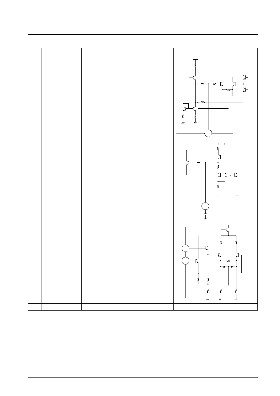
Continued from preceding page.
Pin No.
Pin
Description
Equivalent circuit
16
1st SIF AGC FILTER
∑ First SIF AGC filter connection.
This IC adopts an average value AGC technique. The first
SIF conversion gain is about 30 dB, and the AGC range is
over 50 dB. A 0.01 µF capacitor is normally used in filter
connected to this pin.
∑ When used in an intercarrier system:
Connect this pin (pin 16) to ground. The IC internal switch
will operate to connect the intercarrier output to the SIF
converter input.
16
1k
1k
INTER/SPLIT SW
LO=INTER
A13691
17
IF AGC FILTER
∑ IF AGC filter connection
The signal peak-detected by the built-in AGC detector is
converted to the AGC voltage at pin 17. Additionally, a
second AGC filter (a lag-lead filter) used to create the dual
time constants is provided internally in the IC.
Use a 0.022-µF capacitor as the external capacitor, and
adjust the value according to the sag, AGC speed, and
other characteristics.
17
1k
A13692
18
19
VIF input
∑ VIF amplifier input.
The input circuit is a balanced circuit, and the input circuit
constants are:
R
1.5 k
C
3 pF
18
19
A13693
20
GND
Continued on next page.
No. 6803-12/14
LA7567GM
Continued from preceding page.
Pin No.
Pin
Description
Equivalent circuit
21
RF AGC VR
∑ RF AGC VR connection.
This pin sets the tuner RF AGC operating point. Also, the
FM output and the video output can both be muted at the
same time by connecting this pin to ground.
20k
20k
560
A13694
21
4.2V
22
NICAM output
∑ First SIF output.
Internally, this is an emitter-follower output with a 600-
resistor attached. When used in an intercarrier system, the
buzz characteristics can be improved by forming a
chrominance carrier trap with this pin.
22
20k
20k
6k
620
23
FM filter
∑ Connection for a filter used to hold the FM detector output
DC voltage fixed. Normally, a 1-µF electrolytic capacitor
should be used. The capacitance should be increased if
the low band (around 50 Hz) frequency characteristics
need to be improved.
∑ The FM detector output level can be reduced and the FM
dynamic range can be increased by inserting a resistor and
a capacitor in series between pin 23 and ground.
1k
1k
A13696
23
C
+
R
24
FM Detector output
∑ Audio FM detector output. A 300-
resister is inserted in
series with an emitter-follower output.
∑ For applications that support stereo:
Applications that input this signal to a stereo decoder may
find that the input impedance is reduced, the left and right
signals are distorted, and that the stereo characteristics are
degraded. If this problem occurs, add a resistor between
pin 24 and ground.
R1
5.1 k
∑ For applications that support mono:
Create an external deemphasis circuit.
t = C
◊
R2
R2
300
3.3k
C
R1
A13697
24
22
A13695
Forms a chrominance killer trap.

Notes on Sanyo SAW Filters
There are two types of SAW filters, which differ in the piezoelectric substrate material, as follows:
∑ Lithium tantalate (LiTaO3) SAW filter
TSF11
s
s s
s
... Japan
TSF12
s
s s
s
... US
Although lithium tantalate SAW filters have the low temperature coefficient of ≠18 ppm/∞C, they suffer from a large
insertion loss. However, it is possible, at the cost of increasing the number of external components required, to
minimize this insertion loss by using a matching circuit consisting of coils and other components at the SAW filter
output. At the same time as minimizing insertion loss, this technique also allows the frequency characteristics, level,
and other aspects to be varied, and thus provides increased circuit design flexibility. Also, since the SAW filter
reflected wave level is minimal, the circuit can be designed with a small in-band ripple level.
∑ Lithium niobate (LiNbO3) SAW filter
TSF52
s
s s
s
... US
TSF53
s
s s
s
... PAL
Although lithium niobate SAW filters have the high temperature coefficient of ≠72 ppm/∞C, they feature an insertion
loss about 10 dB lower than that of lithium tantalate SAW filters. Accordingly, there is no need for a matching circuit
at the SAW filter output. Although the in-band ripple is somewhat larger than with lithium tantalate SAW filters, since
they have a low impedance and a small field slew, they are relatively immune to influences from peripheral circuit
components and the geometry of the printed circuit board pattern. This allows stable out-of-band trap characteristics to
be acquired. Due to the above considerations, lithium tantalate SAW filters are used in applications for the US and
Japan that have a high IF frequency, and lithium niobate SAW filters are used in PAL and US applications that have a
low IF frequency.
Notes on SAW Filter Matching
In SAW filter input circuit matching, rather than matching the IF frequency, flatter video band characteristics can be
acquired by designing the tuning point to be in the vicinity of the audio carrier rather than near the chrominance carrier.
The situation shown in figure on the right makes it easier to acquire flat band characteristics than that in figure on the
left.
With the Tuning Set to the IF frequency
With the Tuning Set to the Vicinity of S and C
No. 6803-13/14
LA7567GM
A13698
Coil Specifications
The high band is reduced
SAW filter
characteristics
The high band is extended
Frequency
Frequency
Toko Co., Ltd. 2-1-17 Higashi-yukigaya, Ohta-ku, Tokyo, Japan
TEL: +81-3-3727-1167
JAPAN f = 58.75 MHz
US f = 45.75 MHz
PAL f = 38.9 MHz
VCO coil
Test production no. V291XCS-3220Z
Test production no. 291XCS-3188Z
Test production no. 292GCS-7538Z
Toko Co., Ltd.
Toko Co., Ltd.
Toko Co., Ltd.
SAW filter
Picture
Picture
Picture
(SPLIT)
TSF1137U
TSF1241
TSF5315
Sound
Sound
Sound
SAW filter
TSF5220
TSF5321
(INTER)
TSF5221
TSF5344
S
t = 5 t
0.12 ¯
C = 24 pF
A12048
S
t = 6 t
0.12 ¯
C = 24 pF
A12049
S
t = 7 t
0.12 ¯
C = 24 pF
A12050
PS No. 6803-14/14
LA7567GM
This catalog provides information as of December, 2001. Specifications and information herein are
subject to change without notice.
Specifications of any and all SANYO products described or contained herein stipulate the performance,
characteristics, and functions of the described products in the independent state, and are not guarantees
of the performance, characteristics, and functions of the described products as mounted in the customer's
products or equipment. To verify symptoms and states that cannot be evaluated in an independent device,
the customer should always evaluate and test devices mounted in the customer's products or equipment.
SANYO Electric Co., Ltd. strives to supply high-quality high-reliability products. However, any and all
semiconductor products fail with some probability. It is possible that these probabilistic failures could
give rise to accidents or events that could endanger human lives, that could give rise to smoke or fire,
or that could cause damage to other property. When designing equipment, adopt safety measures so
that these kinds of accidents or events cannot occur. Such measures include but are not limited to protective
circuits and error prevention circuits for safe design, redundant design, and structural design.
In the event that any or all SANYO products (including technical data, services) described or contained
herein are controlled under any of applicable local export control laws and regulations, such products must
not be exported without obtaining the export license from the authorities concerned in accordance with the
above law.
No part of this publication may be reproduced or transmitted in any form or by any means, electronic or
mechanical, including photocopying and recording, or any information storage or retrieval system,
or otherwise, without the prior written permission of SANYO Electric Co., Ltd.
Any and all information described or contained herein are subject to change without notice due to
product/technology improvement, etc. When designing equipment, refer to the "Delivery Specification"
for the SANYO product that you intend to use.
Information (including circuit diagrams and circuit parameters) herein is for example only; it is not
guaranteed for volume production. SANYO believes information herein is accurate and reliable, but
no guarantees are made or implied regarding its use or any infringements of intellectual property rights
or other rights of third parties.
Notes on VCO Tank Circuits
∑ Built-in capacitor VCO tank circuits
When the power is turned on, the heat generated by the IC is transmitted through the printed circuit board to the VCO
tank circuit. At this point, the VCO coil frame functions as a heat sink and the IC heat is dissipated. As a result, it
becomes more difficult to transmit heat to the VCO tank circuit's built-in capacitor, and the influence of drift at power
on is reduced. Therefore, it suffices to design the circuit so that the coil and capacitor thermal characteristics cancel.
Ideally, it is better to use a coil with a core material that has low temperature coefficient characteristics.
∑ External capacitor VCO tank circuits
When an external capacitor is used, heat generated by the IC is transmitted through the printed circuit board directly to
the VCO tank circuit external capacitor. While this capacitor is heated relatively early after the power is turned on, the
coil is not so influenced as much by this heat, and as a result the power-on drift is increased. Accordingly, a coil whose
core material has low temperature coefficient characteristics must be used. It is also desirable to use a capacitor with
similarly low temperature coefficient characteristics.
Note: Applications that use an external capacitor here must use a chip capacitor. If an ordinary capacitor is used,
problems such as the oscillator frequency changing with the capacitor orientation may occur.