 | –≠–ª–µ–∫—Ç—Ä–æ–Ω–Ω—ã–π –∫–æ–º–ø–æ–Ω–µ–Ω—Ç: LA7578N | –°–∫–∞—á–∞—Ç—å:  PDF PDF  ZIP ZIP |
Document Outline
- LA6511
- LA6524
- LA6530M
- LA6537M
- ˇ˛
- LA7583
- LA7625, 7626
- LA7832
- LA7833
- LA8608V
- LB1640N
- LB1837M
- LB1839M

IF Signal Processing (Super PLL-II VIF + SIF)
Circuit for TVs and VCRs
Overview
The LA7578N is an intercarrier-type VIF + SIF IC that
supports excellent sound quality and image quality.
The pin assignment of the LA7578N is identical to that of the
LA7577N, allowing the LA7577N to be used for split systems
while the LA7578N is used for intercarrier systems. In
addition, the LA7578N suppresses Nyquist buzz interference
by using a PLL detection system with a buzz canceller in order
to provide the best sound quality possible.
Functions
[VIF Block]
.
VIF amplifier
.
PLL detector
.
VCO
.
Equalizer amplifier
.
APC filter
.
Lock detection
.
B/W NC
.
RF AGC
.
AFT
.
APC detector
.
IF AGC
.
Buzz canceller
[SIF Block]
.
Limiter amplifier
.
FM quadrature detector
[Mute]
.
Audio mute (pin 2)
.
AV mute (pin 4)
.
IS-15 switch (pin 13)
Package Dimensions
unit : mm
3067-DIP24S
[LA7578N]
SANYO : DIP24S
Features
.
Excellent buzz and buzz-beat characteristics due to PLL
detection system with buzz canceller.
.
Built-in APC time constant switch.
.
Duplicate time constant system suited for high-speed AGC.
.
Excellent DG and DP characteristics.
.
RF AGC adjustment is simple.
Ordering number: EN 4952
Monolithic Linear IC
LA7578N
SANYO Electric Co.,Ltd. Semiconductor Bussiness Headquarters
TOKYO OFFICE Tokyo Bldg., 1-10, 1 Chome, Ueno, Taito-ku, TOKYO, 110 JAPAN
81095HA (II)No.4952 - 1/18
Specifications
Maximum Ratings
at Ta = 25 ∞C
Parameter
Symbol
Conditions
Ratings
Unit
Maximum supply voltage
V
CC
max
13.8
V
Allowable power dissipation
Pd max
Ta
%
50 ∞C
1200
mW
Circuit voltage
V
3
, V
13
V
CC
V
V
14
V
CC
V
Circuit current
I
1
≠1
mA
I
17
≠10
mA
I
21
≠3
mA
I
10
3
mA
Operating temperature
Topr
Note 1
≠20 to +70
∞C
Storage temperature
Tstg
≠55 to +150
∞C
Note : The current that flows into the IC is positive (no signal); the current that flows out of the IC is negative.
Note 1 : ≠20 to +75 ∞C at V
CC
= 9 V
Operating Conditions
at Ta = 25 ∞C
Parameter
Symbol
Conditions
Ratings
Unit
Recommended supply voltage
V
CC
9 or 12
V
Operating supply voltage range
V
CC
op
8.2 to 13.2
V
Note:
.
Always turn on the protective resistance when drawing a line directly out from the IC at usage. (Pins 2, 11, 12, etc.)
.
A capacitor with favorable humidity characteristics should be used for pin 13. (ex. OS capacitor)
.
Pin 8 (NC) should always be open.
Operating Characteristics
at Ta = 25 ∞C, V
CC
= 12 V
Parameter
Symbol
Conditions
min
typ
max
Unit
[VIF Block]
Circuit current
I
9
V
13
= 5 V, S1 = ON
42
48
57
mA
No-signal video output voltage
V
21
V
13
= 5 V, S1 = ON
6.6
7
7.4
V
Maxinum RF AGC voltage
V
10H
V
13
= 7 V, S1 = OFF
10.6
11
11.4
V
Mininum RF AGC voltage
V
10L
V
13
= 7 V, S1 = ON
0
0.5
V
No-signal AFT voltage
V
14
V
13 = 5 V, S1 = ON
3.0
5.9
8.0
V
Input sensitivity
Vi
S1 = OFF
33
39
45
dB/µV
AGC range
GR
S1 = ON
60
66
dB
Maxinum allowable Input
Vi max
S1 = ON
100
105
dB/µV
Video output amplitude
V
O
(video)
S1 = ON
1.95
2.25
2.55
Vp-p
Output S/N
S/N
S1 = ON
49
55
dB
Sync signal tip voltage
V
21
(tip)
Vi = 10 mV, S1 = ON
4.15
4.45
4.75
V
920 kHz beat level
I
920
P = 0, C = ≠4 dB, S = ≠14 dB, S1 = ON
37
43
dB
Frequency characteristics
fc
P = 0, S = ≠14 dB
6
8
MHz
Differential gain
DG
Vi = 10 mV, 87.5% mod,
fp = 58.75 MHz
3
6
%
Differential phase
DP
2
5
deg
Maxinum AFT voltage
V
14H
11
11.5
12
V
Mininum AFT voltage
V
14L
0
0.4
1.0
V
White noise threshold voltage
V
WTH
8.9
9.3
9.7
V
White noise clamp voltage
V
WCL
5.3
5.7
6.1
V
Black noise threshold voltage
V
BTH
S1 = ON
3.4
3.7
4.0
V
Black noise clamp voltage
V
BCL
S1 = ON
5.3
5.7
6.1
V
Continued on next page.
LA7578N
No.4037-2/18
Continued from preceding page.
Parameter
Symbol
Conditions
min
typ
max
Unit
AFT detection sensitivity
Sf
50
70
100
mV/kHz
VIF input resistance
Ri (VIF)
f = 58.75 MHz
0.8
1.3
1.75
k
VIF input capacity
Ci (VIF)
f = 58.75 MHz
3.0
6.0
pF
APC pull-in range (U)
f
PU
-2
S1 = ON
0.6
1.6
MHz
APC pull-in range (L)
f
PL
-2
S1 = ON
≠1.6
≠0.8
MHz
VCO maximum variable range
f
U
V
18 = 3 V, S1 = ON
0.6
1.6
MHz
f
L
V
18 = 7 V, S1 = ON
≠1.6
≠0.8
MHz
VCO control sensitivity
V
18 = 5 V to 4.6 V
1.5
3.1
6.2
kHz/mV
SIF output signal voltage
V
O
(SIF)
P/S = 20 dB
120
170
240
mVrms
[SIF Block] : V13 = 5 V
SIF limiting sensitivity
Vi (lim)
33
39
dB/µV
FM detection output voltage
V
O
400
600
790
mVrms
AMR
AMR
40
49
dB
Distortion
THD
0.5
1.0
%
SIF S/N
S/N (SIF)
60
78
dB
[Mute Defeat]
AFT defeat start voltage
VD
11
0.5
2.3
V
AV mute
V
4TH
0.5
1.9
V
FM mute
V
2TH
0.5
2.0
V
AFT defeat voltage
VD
14
5.4
6
6.6
V
Operating Characteristics
at Ta = 25 ∞C, V
CC
= 9 V
Parameter
Symbol
Conditions
min
typ
max
Unit
[VIF Block]
Circuit current
I
9
V
13
= 5 V, S1 = ON
36
41
49
mA
No-signal video output voltage
V
21
V
13
= 5 V, S1 = ON
5.0
5.4
5.8
V
Maxinum RF AGC voltage
V
10H
V
13
= 7 V, S1 = OFF
7.6
8
8.4
V
Mininum RF AGC voltage
V
10L
V
13
= 7 V, S1 = ON
0
0.5
V
No-signal AFT output voltage
V
14
V
13
= 5 V, S1 = ON
2.6
4.5
6.0
V
Input sensitivity
Vi
S1 = OFF
37
43
49
dB/µV
Video output amplifude
V
O
(video)
S1 = OFF
1.5
1.75
2.0
Vp-p
Sync signal tip voltage
V
21
(tip)
Vi = 10 mV, S1 = ON
3.25
3.55
3.85
V
Maximum AFT voltage
V
14H
8
8.5
9.0
V
Minimum AFT voltage
V
14L
0.3
1.0
V
White noise threshold voltage
V
WTH
6.8
7.2
7.6
V
White noise clamp voltage
V
WCL
4.0
4.4
4.8
V
Black noise threshold voltage
V
BTH
S1 = ON
2.5
2.8
3.1
V
Black noise clamp voltage
V
BCL
S1 = ON
3.7
4.1
4.5
V
AFT detection sensitivity
Sf
30
43
60
mV/kHz
SIF output signal voltage
V
O
(SIF)
P/S = 20 dB
90
130
180
mVrms
[SIF Block]
FM detection output voltage
V
O
V
13
= 5 V
400
600
790
mVrms
[Mute defeat voltage]
AFT defeat start voltage
VD
11
0.5
1.6
V
AV mute
V
4TH
0.5
1.1
V
FM mute
V
2TH
0.5
1.9
V
AFT defeat voltage
VD
14
3.9
4.5
5.1
V
LA7578N
No.4037-3/18
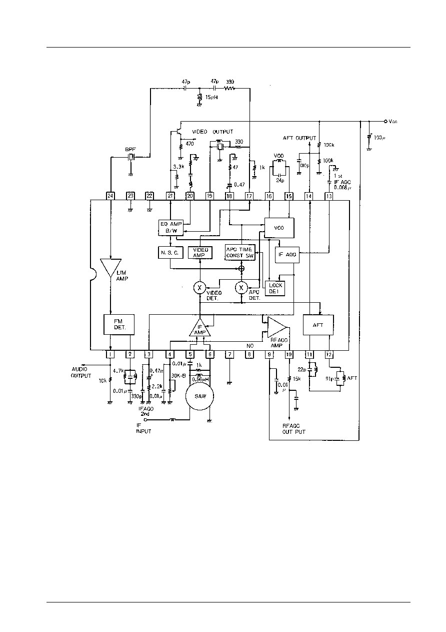
Sample Application Circuit (JAPAN)
Unit (resistance :
, capacitance: F)
Pins 22 and 23 are grounded inside the IC.
LA7578N
No.4037-4/18
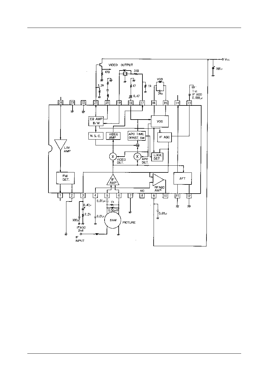
Sample Application Circuit (JAPAN)
When using no SIF, 1stSIF, AFT, RFAGC.
Unit (resistance :
, capacitance : F)
1.
When using no SIF circuit:
Pin1 = Open
Pin2 = GND
Pin24 = Open
2.
When using no AFT circuit:
Pin11, 12 = GND
Pin14 = Open
3.
When using no RFAGC circuit:
Connect a capacitor of 0.01 µF across Pin 4 and GND.
Pin10 = Open
LA7578N
No.4037-5/18