 | –≠–ª–µ–∫—Ç—Ä–æ–Ω–Ω—ã–π –∫–æ–º–ø–æ–Ω–µ–Ω—Ç: LA7615 | –°–∫–∞—á–∞—Ç—å:  PDF PDF  ZIP ZIP |

Ordering number : ENN5841
91799RM (OT) No. 5841-1/39
Overview
The LA7615 is an NTSC color TV IC that supports
computer control over an I
2
C bus. In addition to improved
quality and increased functionality in color TV products,
this IC supports the development of a TV set product line
in software and the simplification of end product design.
The provision of an I
2
C bus means that this product can
also respond to desires for increased total manufacturing
productivity, including improved automation of computer
controlled production lines.
Functions
∑ I
2
C bus control, VIF, SIF, Y, C, and deflection circuits
integrated on a single chip.
Features
∑ Pursuit of higher integration levels
The LA7615 integrates VIF, SIF, luminance,
chrominance, and deflection (horizontal and vertical
synchronization) circuits, A/V switching, and power
supply control on a single chip.
∑ Bus control for reduced external component counts and
mechanical adjustment points
All the LA7615 signal-processing circuits can be
controlled and adjusted digitally over the I
2
C bus. All
adjustments, both those required during manufacture and
the user controls, can be controlled over the I
2
C bus, and
both function selection and characteristics settings can
be performed in software over the I
2
C bus. This
increases flexibility in designing a product line of TV
sets and also enhances productivity by allowing mixed
production runs.
While this device supports multifunction and good
performance, it is also economical in that it achieves
reduced power and reduced pin count.
Package Dimensions
unit: mm
3071-DIP64S
57.2
0.95
0.48
1.78
1.01
4.0
0.51min
5.0max
19.05
16.8
0.25
3.2
33
64
32
1
SANYO: DIP64S
[LA7615]
LA7615
SANYO Electric Co.,Ltd. Semiconductor Company
TOKYO OFFICE Tokyo Bldg., 1-10, 1 Chome, Ueno, Taito-ku, TOKYO, 110-8534 JAPAN
Single-Chip NTSC Color TV IC
Monolithic Linear IC
Any and all SANYO products described or contained herein do not have specifications that can handle
applications that require extremely high levels of reliability, such as life-support systems, aircraft's
control systems, or other applications whose failure can be reasonably expected to result in serious
physical and/or material damage. Consult with your SANYO representative nearest you before using
any SANYO products described or contained herein in such applications.
SANYO assumes no responsibility for equipment failures that result from using products at values that
exceed, even momentarily, rated values (such as maximum ratings, operating condition ranges, or other
parameters) listed in products specifications of any and all SANYO products described or contained
herein.

No. 5841-2/39
LA7615
Parameter
Symbol
Conditions
Ratings
Unit
V2 max
9.6
V
Maximum supply voltage
V17 max
9.6
V
V32 max
9.6
V
V60 max
9.6
V
Maximum supply current
I24 max
30
mA
Allowable power dissipation
Pd max
Ta
65∞C
1.5
W
Operating temperature
Topr
≠10 to +65
∞C
Storage temperature
Tstg
≠55 to +150
∞C
Specifications
Maximum Ratings
at Ta = 25∞C
Parameter
Symbol
Conditions
Ratings
Unit
V2
7.6
V
Recommended supply voltage
V17
7.6
V
V32
7.6
V
V60
7.6
V
Recommended supply current
I24
24
mA
V2 op
7.3 to 7.9
V
Operating supply voltage range
V17 op
7.3 to 7.9
V
V32 op
7.3 to 7.9
V
V60 op
7.3 to 7.9
V
Operating supply current range
I24 op
20 to 30
mA
Operating Conditions
at Ta = 25∞C
Functional Description
<VIF/SIF Functions>
In addition to a PLL synchronous detection system, the IF block also adopts a split system in which the VIF signal and
the SIF signal are processed separately.
∑ Low-level VCO
The LA7615 achieves a significant reduction in beat generation due to interference by lowering the VCO oscillator
level from that used in earlier ICs.
∑ Adjustment-free VCO coil implemented using bus control
By compensating for manufacturing variations in the VCO coil using bus control, the LA7615 eliminates coil
adjustment from the manufacturing line.
∑ Built-in 4.5 MHz trap
The LA7615 incorporates an on-chip trap that also provides a video equalizer function. Thus the number of external
trap, inductor, and capacitor components is reduced.
∑ Built-in SIF FM detector: 4.5 MHz quadrature detection
∑ The video signal and FM demodulated signal levels can be controlled from the serial bus.
The improved precision associated with controlling the output level over the serial bus makes it easier to design the
interface with the following stage.
∑ Built-in buzz canceler
Allows high performance to be maintained even during stereo reception.
∑ Built-in video switch (INT/EXT(AUX) switching circuit)
Built-in AUX input switching circuit means that the dedicated switching ICs required can be reduced. Also, the ability to
control this switch from the serial bus makes it easier to design the peripheral wiring pattern.
∑ Dedicated IF video signal output pin
The provision of this pin makes it easier to design end products that support PIP and similar features.
<Luminance and Chrominance Circuits>
These blocks have been designed to minimize the use of external components as much as possible. The filter circuits are
now integrated on the same chip, and not only the adjustment circuits, but also the function selection and characteristics
modifications functions can be controlled over the serial bus. As a result, basically all the signal processing from input to
output can be performed with only the addition of the chrominance circuit VCO crystal and the APC filter circuit.
Furthermore, this IC also supports high image quality systems and responds to needs from a diverse range of end
products.
∑ Two independent inputs for the luminance and chrominance signals and switching between the Y1/C1 and Y2/C2 inputs
∑ Video muting on/off switch
∑ Built-in filters (The filter f0 adjustment function can be used to select the filter characteristics.)
Chrominance system: Bandpass filter (symmetric and asymmetric types)
Luminance system: Color trap and delay line
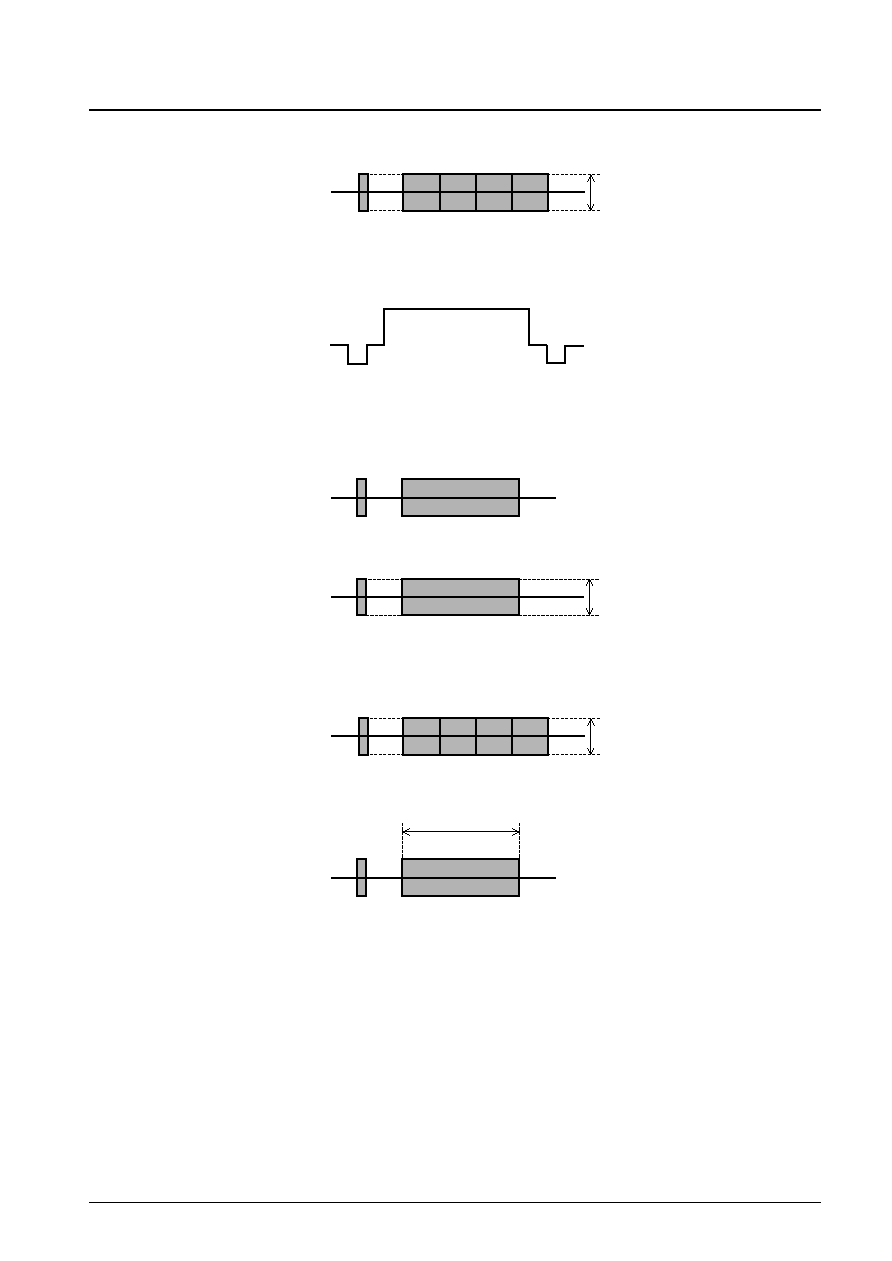
<Luminance System Circuit>
∑ Built-in high image quality variable-type luminance system filter (color trap and delay line)
Luminance filter mode selection (f0 adjustment)
Four modes are provided: 3.58 MHz trap, 4.2 MHz trap, 5.0 MHz wide, and 10.0 MHz high band.
∑ Peaking (sharpness) control
Aperture type control implemented using the delay line
The emphasis frequency is automatically selected according to the f0 mode using the delay line.
One of the four frequencies 2.2, 2.6, 3.0, or 4.9 MHz is emphasized according to which of the f0 modes (3.58 MHz
trap, 4.2 MHz trap, 5.0 MHz wide, or 10.0 MHz high band) is used.
∑ Adaptive coring
For low-level signals, the above peaking is suppressed to reduce the image contamination due to that peaking.
The coring level is automatically adjusted according to the amplitude of the input signal.
∑ Black stretch circuit: Can be turned on or off under control of the serial bus interface.
∑ SYO (Selected luminance (Y) output)
One of the Y1/Y2 inputs is selected, and that input signal is output as the sync separator circuit signal directly.
However, the DC level of that signal is clamped at 1/2 VCC.
Also, this signal can be used for closed captions or as a velocity modulation.
∑ Support for analog/digital OSD
Amplitude level limiting is applied to digital input signals internally to the IC.
∑ Contrast and brightness controls
∑ ABL (automatic beam limiter)
Three-pin system (IB IN, BRT ABL FILT, and CONTRAST ABL FILT pins), mode switching under control of serial
bus data.
∑ R, G, and B output drive and bias adjustments
∑ Sub-bias (brightness) control
The DC level of each of the R, G, and B signals can be adjusted over a 4-step (2-bit) range.
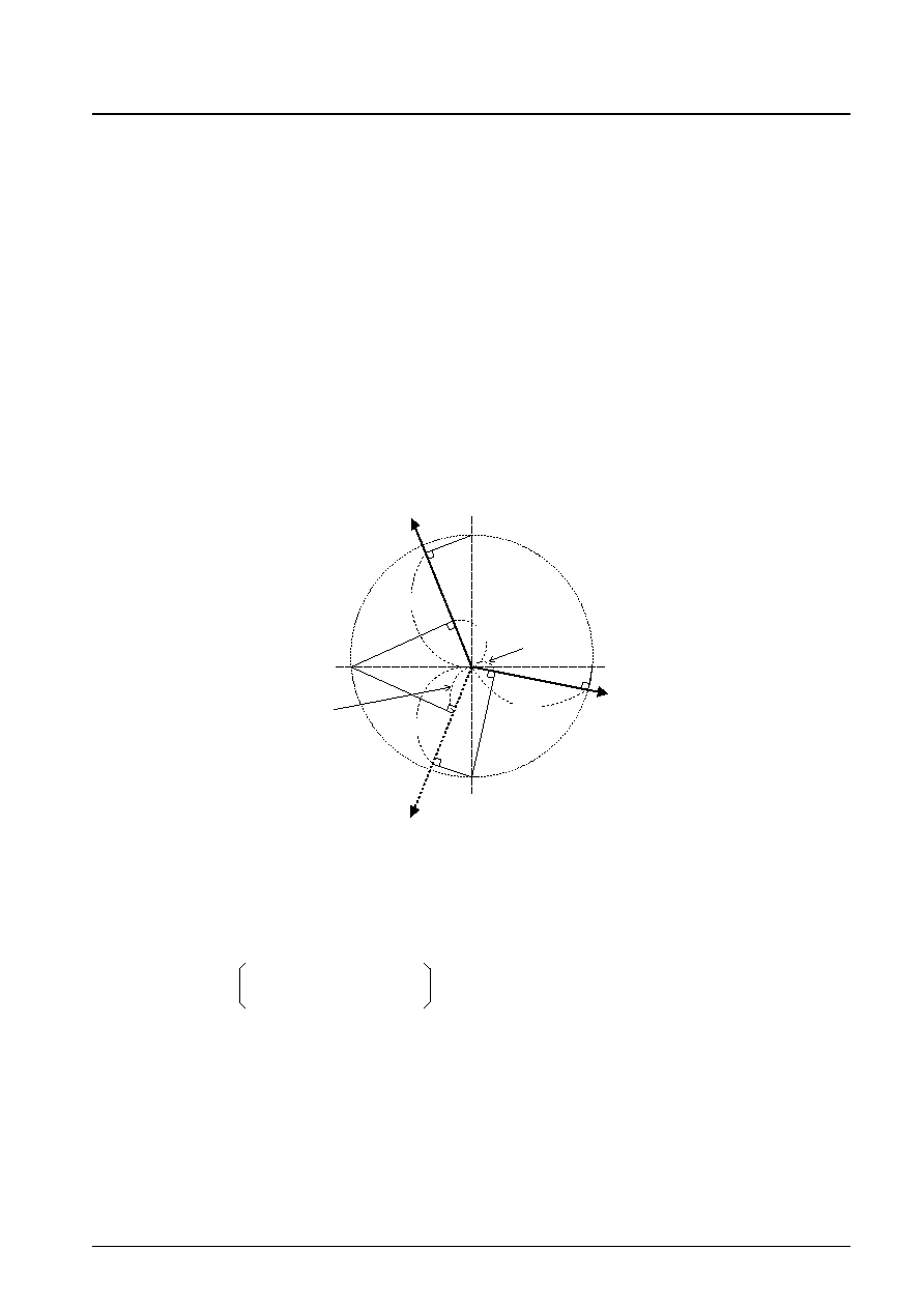
<Chrominance Circuit>
∑ Built-in chrominance bandpass filter
Chrominance system filter mode selection: bandpass filter peaking/symmetric type selection and chrominance
bandpass filter bypass on/off setting
∑ Auto Flesh: Flesh tone correction (on/off)
∑ Overload (on/off)
Limits the saturation of the color when the ratio of the burst and color signals is large, i.e. when the color is highly
saturated.
∑ Color phase and saturation controls
∑ Demodulation angle: 104∞
No. 5841-3/39
LA7615
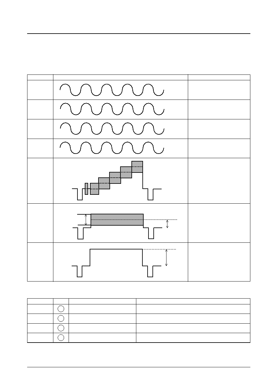
<f0 Mode Selection>
*
: Reference values
Mode f0 =
Y signal
Chroma signal
Trap f0
*
Total delay
BPF
*
Total 500 ns delay
0
3.58 MHz
500 ns
Asymmetric (peaking type)
515 ns
1
4.2 MHz
510 ns
Symmetric
535 ns
2
5.0 MHz
520 ns
3
10.0 MHz
265 ns
Bypass
265 ns

<Deflection Circuits>
Dedicated sync separator circuit input pin
The horizontal deflection circuit adopts a dual AFC circuit, and the horizontal oscillator uses the 32fH (503 kHz) pulse
signal as the horizontal decrement counter clock.
The following are the main settings for the horizontal output system that can be controlled over the serial bus interface.
These settings support even more efficient end product design.
∑ AFC gain (first loop gain control)
∑ APC gain (second loop gain control)
∑ Horizontal duty cycle
∑ Horizontal phase
*: The vertical deflection circuit adopts a decrement counter system, and provides constantly adjustment-free and stable
vertical synchronization for any type of signal, from TV on air, to weak reception conditions, to VCR signals.
Furthermore, this circuit uses an internal capacitor to implement a ramp generator, and allows the corrections
described later in this document to be applied to correct image distortion and other problems due to manufacturing
variations in the TV tube itself.
<Horizontal Circuit Functions>
∑ High-stability adjustment-free horizontal oscillator that uses a ceramic oscillator element
∑ Dual AFC circuit
∑ Multi-mode control of the AFC gain (first loop gain)
∑ Horizontal duty and phase controls
∑ Geometrical distortion correction: East-west DC (horizontal size)
East-west amplitude (horizontal pin-cushion distortion correction)
Corner pin
East-west corner 1
East-west corner 2
Tilt adjustment
∑ Sync killer
<Vertical Circuit Functions>
∑ Forcible non-standard mode support (standard mode: 262.5 H)
∑ Vertical size/linearity and vertical DC (vertical position) adjustments, vertical S-curve correction
∑ V-comp adjustment (Corrects for changes in the vertical size due to variations in the luminance.)
∑ Vertical killer
<Power System>
PWM circuits have come to be widely used in TV set power supplies in recent years. This IC integrates parts of the
power supply circuit (the pulse generator and its control system) and allows the supply voltage (high B) to be adjusted
over the serial bus.
No. 5841-4/39
LA7615
No. 5841-5/39
LA7615
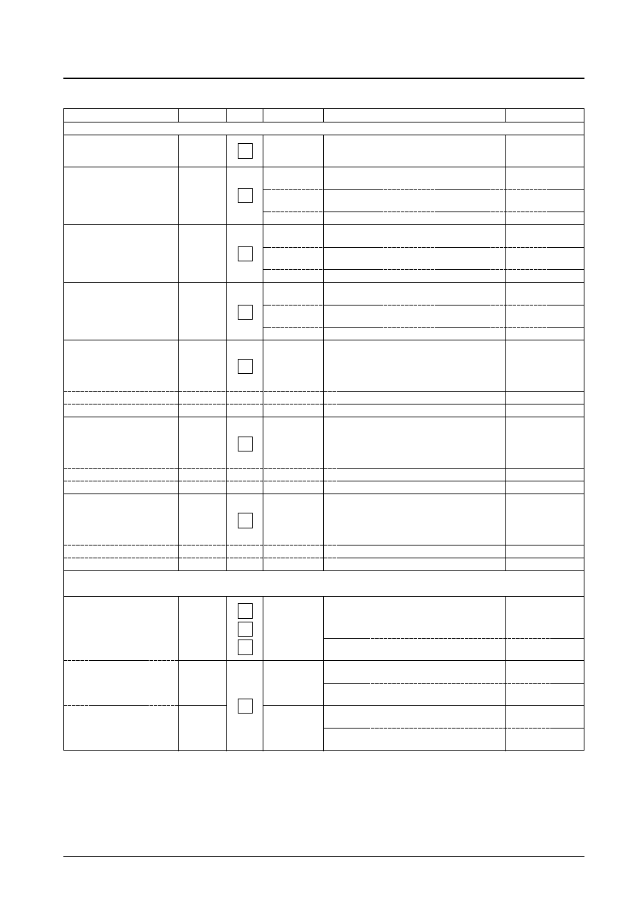
Bus Control
General Functions
ON/OFF SW
1 bit
Video muting switch
1 bit
VIF/SIF
Video signal switching
1 bit
RF AGC delay
6 bits
IF AGC SW
1 bit
PLL tuning
7 bits
APC detector adjustment
6 bits
AFT defeat switch
1 bit
Noise inverter defeat switch
1 bit
Video level
3 bits
Sound 4.5 MHz trap
4 bits
FM level
4 bits
F0 fast (FM detection speed)
1 bit
Luminance/Chrominance Systems
Y/C input selection (one of two inputs) switch
1 bit
Luminance (Y) F0 adjustment (filter control)
2 bits
Chrominance signal bandpass filter mode switch
1 bit
Chrominance signal bandpass filter bypass switch
1 bit
Black stretch on/off switch
1 bit
Peaking (sharpness) control
5 bits
Coring on/off switch
1 bit
Auro flesh on/off
1 bit
Overload switch
1 bit
Contrast control
6 bits
Brightness control
6 bits
Tint control
7 bits
Saturation control
7 bits
RGB bias adjustment
6 bits each
RGB bias adjustment
7 bits each
Sub-brightness control
2 bits each
Brightness ABL operating point control
3 bits
Brightness ABL mode defeat switch
1 bit each
Emergency ABL defeat switch
1 bit
Deflection System
AFC gain (sync killer)
2 bits
APC gain
2 bits
Horizontal duty adjustment
2 bits
Horizontal phase adjustment
4 bits
Geometrical distortion correction
EAST-WEST DC
5 bits
EAST-WEST AMPLITUDE
4 bits
East-west corner 1/2
3 bits each
Tilt adjustment
4 bits
Vertical linearity adjustment
4 bits
Vertical S-curve correction
4 bits
Vertical size adjustment
7 bits
Vertical DC adjustment
6 bits
Standard/nonstandard mode switch
1 bit
VERTICAL KILL
1 bit
V-COMP adjustment
3 bits
DAC REF. (+B TRIM)
4 bits
Others: Status Register
POWER ON RESET
1 bit
X-ray protection switch
1 bit
Horizontal lock detection
1 bit
AFT and RF AGC status discrimination
2 bits each
No. 5841-6/39
LA7615
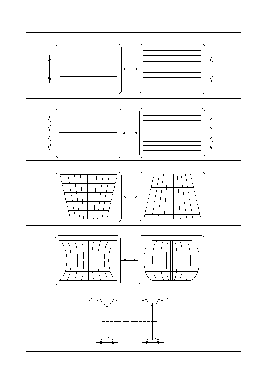
A10048
A10049
A10050
A10051
A10052
Wide
Vertical Linearity
Vertical S-Curve Correction
Tilt
East-West Amp
Corner Pin
The distortion correction operation is symmetric left to right.
Narrow
Narrow
Wide
Wide
Wide
Narrow
Narrow
Narrow
Wide
East-west corner 1
East-west corner 2
No. 5841-7/39
LA7615
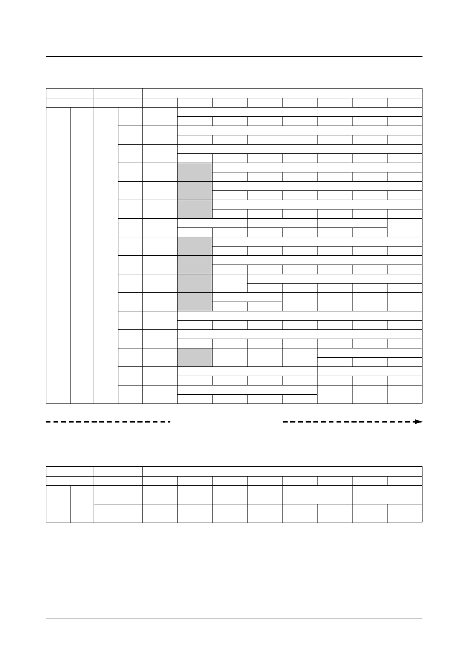
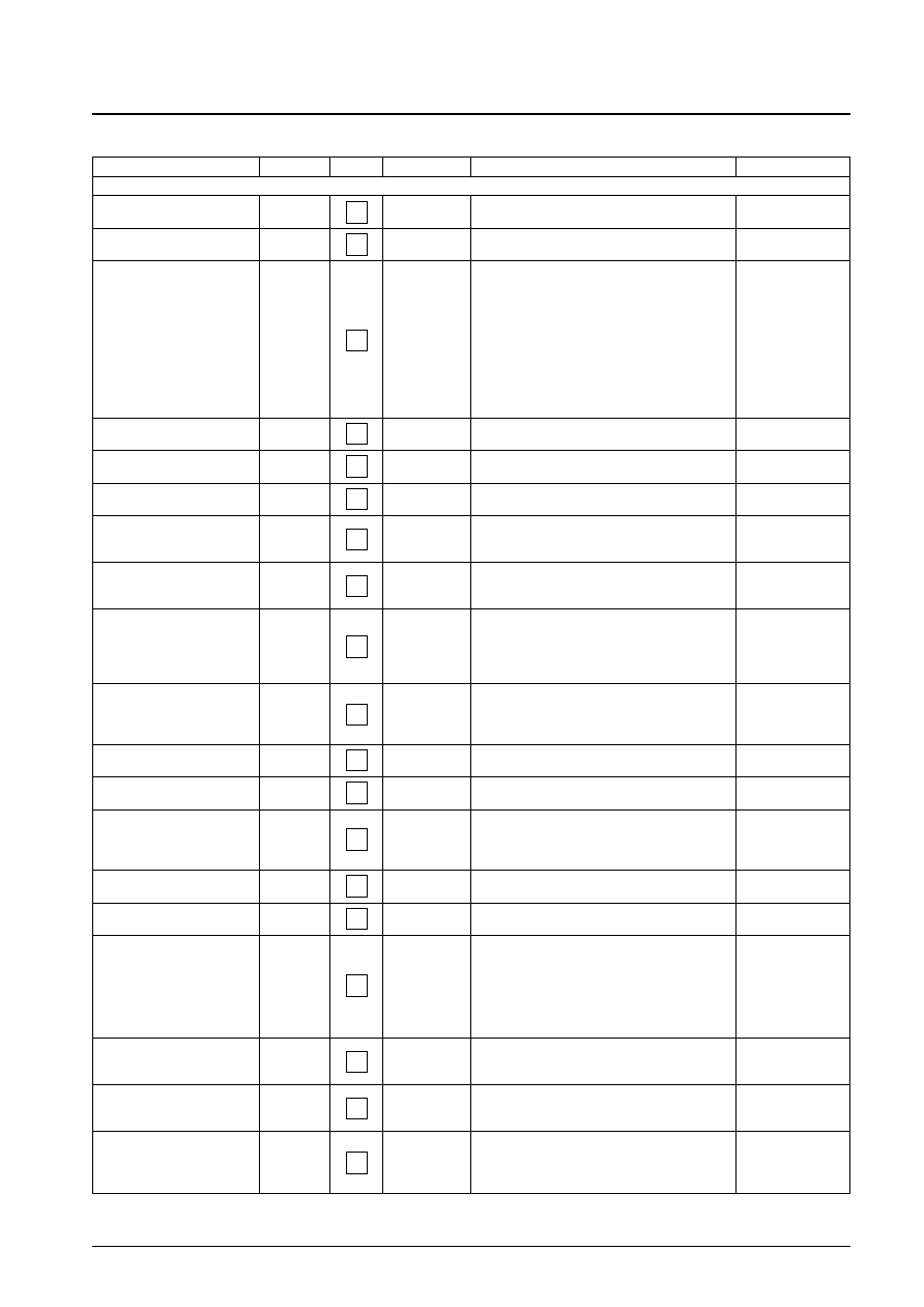
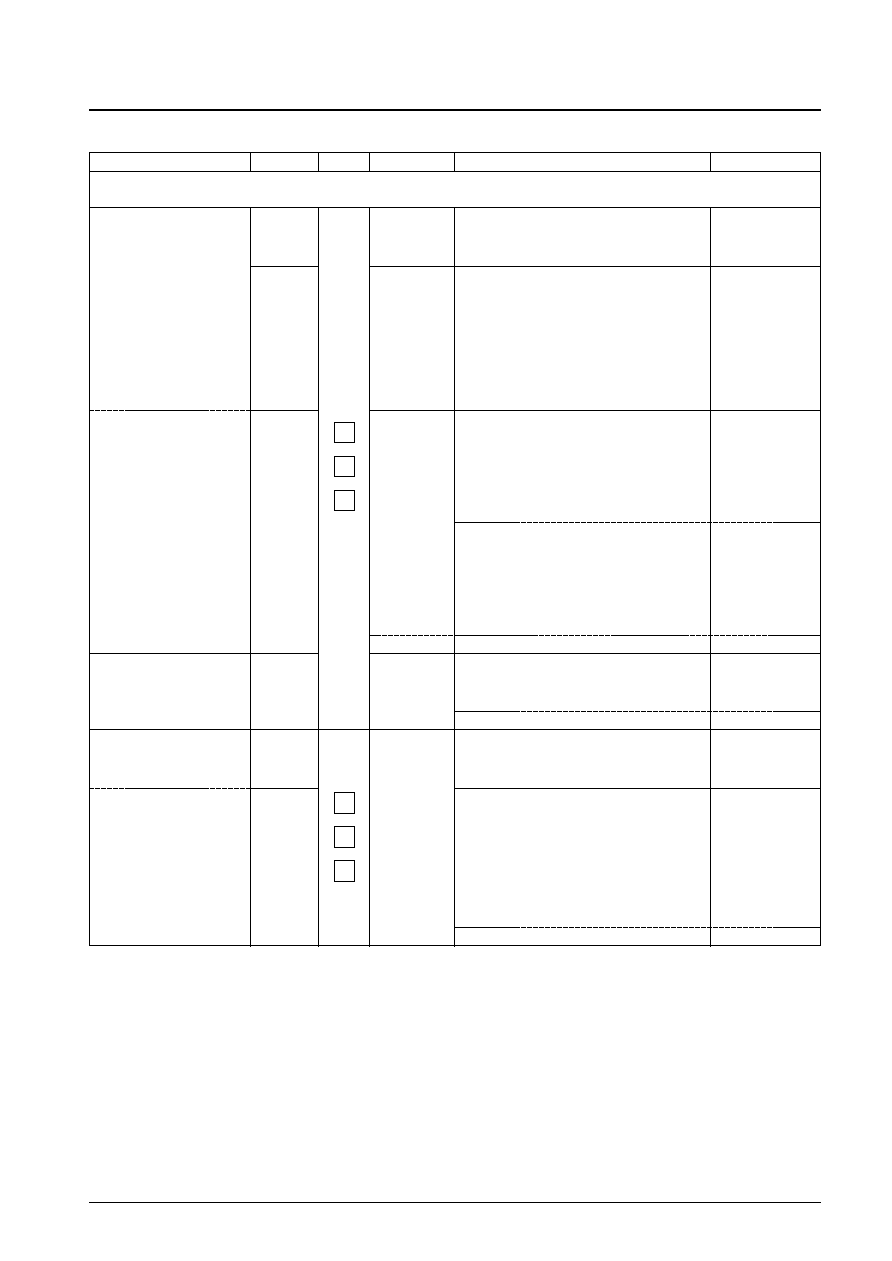
Bus : Control Register Bit Allocation Map
Control Register Bit Allocations
IC address
Sub address
MSB
Data bits
LSB
IC Add7
Add0
• Add7
Add0
Bit 7
Bit 6
Bit 5
Bit 4
Bit 3
Bit 2
Bit 1
Bit 0
1011
1010
0000
0000
1
On/Off
Video
AFC gain/sync kill
mute
(b1)
(b0)
0001
1
APC gain
B+ trim
(b1)
(b0)
(b3)
(b2)
(b1)
(b0)
0010
1
Hor duty cycle
Horizontal phase
(b1)
(b0)
(b3)
(b2)
(b1)
(b0)
0011
1
BNI
RF AGC delay
defeat
(b5)
(b4)
(b3)
(b2)
(b1)
(b0)
0100
1
IF AGC
AFT
FM level
defeat
defeat
(b4)
(b3)
(b2)
(b1)
(b0)
0101
1
VCO free running
(b6)
(b5)
(b4)
(b3)
(b2)
(b1)
(b0)
0110
1
4.5 MHz trap
(b3)
(b2)
(b1)
(b0)
(b2)
(b1)
(b0)
0111
1
Video
IF APC offset adjust.
switch
(b5)
(b4)
(b3)
(b2)
(b1)
(b0)
1000
1
Vertical
Vertical DC
kill
(b5)
(b4)
(b3)
(b2)
(b1)
(b0)
1001
1
Countdown mode
East-west DC
(b1)
(b0)
(b4)
(b3)
(b2)
(b1)
(b0)
1010
1
East-west amp
(b3)
(b2)
(b1)
(b0)
1011
1
Vertical comp.
East-west tilt
(b2)
(b1)
(b0)
(b3)
(b2)
(b1)
(b0)
1100
1
Vertical size
(b6)
(b5)
(b4)
(b3)
(b2)
(b1)
(b0)
1101
1
Vertical linearity
(b3)
(b2)
(b1)
(b0)
1110
1
FM mode
Vertical S-correction
switch
(b3)
(b2)
(b1)
(b0)
1111
1
East-west bottom corner
East-west top corner
(b2)
(b1)
(b0)
(b2)
(b1)
(b0)
Bits are transmitted in this order
No. 5841-8/39
LA7615
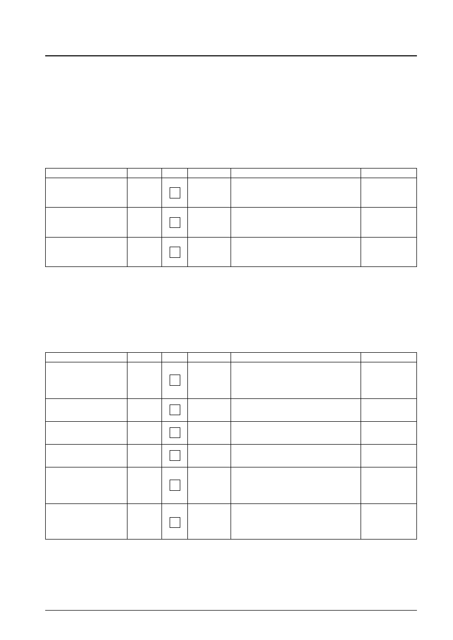
Bus : Control Register Bit Allocation Map
Control Register Bit Allocations (cont)
IC address
Sub address
MSB
Data bits
LSB
IC Add7
0
Add7
Add0
Bit 7
Bit 6
Bit 5
Bit 4
Bit 3
Bit 2
Bit 1
Bit 0
1011
1010
0001
0000
1
Red bias
(b6)
(b5)
(b4)
(b3)
(b2)
(b1)
(b0)
0001
1
Green bias
(b6)
(b5)
(b4)
(b3)
(b2)
(b1)
(b0)
0010
1
Blue bias
(b6)
(b5)
(b4)
(b3)
(b2)
(b1)
(b0)
0011
1
Red drive
(b5)
(b4)
(b3)
(b2)
(b1)
(b0)
0100
1
Green drive
(b5)
(b4)
(b3)
(b2)
(b1)
(b0)
0101
1
Blue drive
(b5)
(b4)
(b3)
(b2)
(b1)
(b0)
0110
1
Blue sub bias
Red sub bias
Green sub bias
Y/C
(b1)
(b0)
(b1)
(b0)
(b1)
(b0)
switch
0111
1
Brightness control
(b5)
(b4)
(b3)
(b2)
(b1)
(b0)
1000
1
Pix control
(b5)
(b4)
(b3)
(b2)
(b1)
(b0)
1001
1
Coring
Peaking control
switch
(b4)
(b3)
(b2)
(b1)
(b0)
1010
1
F0 select
Chroma
Auto
Chrom
Over
(b1)
(b0)
BPF
flesh
bypass
load
1011
1
Tint control
(b6)
(b5)
(b4)
(b3)
(b2)
(b1)
(b0)
1100
1
Color control
(b6)
(b5)
(b4)
(b3)
(b2)
(b1)
(b0)
1101
1
ABL
Mid Stp
EMG
Bright ABL threshold
defeat
defeat
defeat
(b2)
(b1)
(b0)
1110
1
Test register 1
Test register 2
(b3)
(b2)
(b1)
(b0)
(b2)
(b1)
(b0)
1111
1
Test regster 3
Black Stretch
Blanking
Reserved
(b3)
(b2)
(b1)
(b0)
defeat
defeat
IC address
Sub address
MSB
Data bits
LSB
IC Add7
Add0
Add7
Add0
Bit 7
Bit 6
Bit 5
Bit 4
Bit 3
Bit 2
Bit 1
Bit 0
1011
1010
0001
0000
Pon
XRay
Horiz
On/off
AFT status
RF AGC status
lock
0001
1
1
1
1
1
1
1
1
Bits are transmitted in this order
Table 8 : Status Register Bit Allocation Map
Status Register Bit Allocations
No. 5841-9/39
LA7615
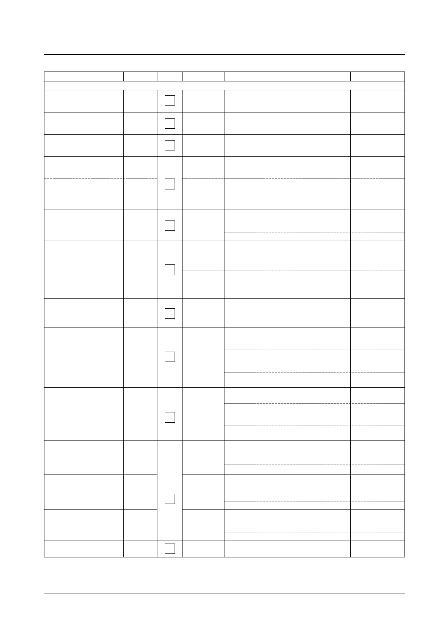
Bus : Control Register Truth Table
Control Register Truth Table
Register
0 HEX
1 HEX
2 HEX
3 HEX
On/off
Off
On
na
na
Video mute
Active
Mute
na
na
AFC gain/sync Kill
Sync Kill
Low gain (auto mode)
Mid gain
High gain
BNI defeat
Enable BNI
Defeat
na
na
IF AGC defeat
Enable AGC
Defeat
na
na
AFT defeat
Enable AFT
Defeat
na
na
Video switch
IF video
Aux video
na
na
Vertical Kill
Vertical active
Vertical Killed
na
na
Countdown mode
Standard
Non-standard
50 Hz
48 Hz
FM mode switch
Normal
Fast
na
na
Y/C switch
Y1/C1 IN
Y2/C2 IN
na
na
Coring switch
Defeat
Enable
na
na
F0 select
3.58 Trap
4.20 Trap
5.00 APF
10.0 APF
Chrom BPF
Symmetrical
Peaker
na
na
Autoflesh
Off
On
na
na
Chroma bypass
BPF
Bypass
na
na
Over load
Off
Active
na
na
Bright ABL defeat
Enable
Defeat
na
na
Bright mid stop defeat
Enable
Defeat
na
na
Emergency ABL defeat
Enable
Defeat
na
na
Black Str defeat
Enable
Defeat
na
na
Blanking defeat
Enable
Defeat
na
na
Bus : Status Register Truth Table
Status Register Truth Table
Register
0 HEX
1 HEX
2 HEX
3 HEX
POR
Inactive
Low standby detected
na
na
XRP
Inactive
XRP fault detected
na
na
Horizontal lock
Locked
Unlocked
na
na
On/off
Off
On
na
na
AFT
IF frequency in high
IF frequency in range
na
IF frequency is low
RF AGC
RF AGC voltage is Low.
RF AGC voltage is in range.
na
RF AGC voltage is High.
No. 5841-10/39
LA7615
Initial Condition
Function
On/off
1 HEX
Video mute
0 HEX
AFC gain & sync Kill
1 HEX
APC gain
3 HEX
B+ trim
8 HEX
Horizontal duty
1 HEX
Horizontal phase
8 HEX
BNI defeat
0 HEX
RF AGC delay
20 HEX
IF AGC defeat
0 HEX
AFT defeat
0 HEX
FM level
10 HEX
IF VCO free running
40 HEX
4.5 trap
8 HEX
Video level
4 HEX
Video switch
0 HEX
IF APC offset
20 HEX
Vertical Kill
0 HEX
Vertical DC
20 HEX
Countdown mode
0 HEX
East/west DC
10 HEX
East/west amplitude
8 HEX
Vertical comp.
0 HEX
East/west tilt
8 HEX
Vertical size
40 HEX
Vertical linearity
8 HEX
FM mode switch
0 HEX
Vertical S-correction
8 HEX
East/west bottom
0 HEX
East/west top corner
0 HEX
Red bias
00 HEX
Green bias
00 HEX
Blue bias
00 HEX
Red drive
3F HEX
Green drive
3F HEX
Blue drive
3F HEX
Blue sub bias
2 HEX
Red sub bias1
2 HEX
Green sub bias
2 HEX
Y/C switch
0 HEX
Brightness control
20 HEX
Pix control
20 HEX
Coring switch
0 HEX
Peaking control
00 HEX
F0 select
1 HEX
Chroma BPF
0 HEX
Autoflesh
0 HEX
Chroma bypass
0 HEX
Over load
0 HEX
Tint control
40 HEX
Color control
40 HEX
Bright ABL defeat
0 HEX
Bright mid stop
0 HEX
Emergency ABL defeat
0 HEX
Bright ABL threshold
0 HEX
Test registers 1, 2, 3
0 HEX
Black strech defeat
1 HEX
Blanking defeat
0 HEX
Power Up Sequence <Reference>
No. 5841-11/39
LA7615
6.3VDC
7.3VDC
3.0VDC
time
2ms
ON/OFF
= 0
ON/OFF
= 1
Mute
= 0
Initialize
TR1 to TR2
Initialize
TR3 to TR31
Standby
Vcc
ON/OFF
BIT
Registers
(TR1-TR2)
XRP BIT
(STATUS)
Pon BIT
(STATUS)
Registers
(TR3-TR31)
Video.Mute
BIT
Run.Vcc
stable
A10053
After Standby Vcc reaches 3.0VDC, the microcontroller has to wait 2ms in order to intitialize the HC Interface in LA7615.
No. 5841-12/39
LA7615
Parameter
Symbol
Conditions
Ratings
Unit
min
typ
max
[Circuit Voltages and Currents]
Horizontal supply voltage
HV
CC
7.2
7.6
8
V
IF power supplly current (V2)
I2 (IFI
CC
)
IF AGC : 5 V
28
43
58
mA
Vertical supply current (V17)
I17 (DEFI
CC
)
10
13
16
mA
Video/chrominance supply current (V32)
I32 (YCI
CC
)
65
85
105
mA
FM supply current (V60)
I60 (FMI
CC
)
5.5
8.5
11.5
mA
[VIF Block]
No signal AFT output voltage
V14
With no input signal
2.8
3.8
4.8
Vdc
No signal video output voltage
V53
With no input signal
4.7
4.9
5.1
Vdc
APC pull-in range (U)
f
PU
After APC, PLL, and D/A converter
1
MHz
adjustment
APC pull-in range (L)
f
PL
After APC, PLL, and D/A converter
1
MHz
adjustment
Maximum RF AGC voltage
V
4H
CW = 91 dBµ, DAC = 0
7.7
8.2
9.0
Vdc
Minimum RF AGC voltage
V
4L
CW = 91 dBµ, DAC = 63
0
0.2
0.4
Vdc
RF AGC Delay Pt (@DAC = 0)
RF
AGC0
DAC = 0
96
dBµ
RF AGC Delay Pt (@DAC = 63)
RF
AGC63
DAC = 63
86
dBµ
Maximum AFT output voltage
V
14H
CW = 93 dBµ, frequency change
6.2
6.5
7.6
Vdc
Minimum AFT output voltage
V
14L
CW = 93 dBµ, frequency change
0.5
0.9
1.2
Vdc
AFT detection sensitivity
Sf
CW = 93 dBµ, frequency change
33
25
17
mV/kHz
4.5 MHz attenuation
T
RAP
V100 kHz/V4.5 MHz
≠35
≠32
dB
Video output amplitude
V
O
53
93 dBµ, 87.5% Video MOD
1.8
2
2.2
Vp-p
Synchronizing signal tip level
V53
TIP
93 dBµ, 87.5% Video MOD
2.4
2.6
2.8
Vdc
Input sensitivity
V
IN
Output ≠3 dB
43
46
dBµ
Vide/sync ratio (@100 dBµ)
V/S
100 dBµ, 87.5% Video MOD
2.4
2.5
3
Differential gain
DG
93 dBµ, 87.5% Video MOD
2
10
%
Differential phase
DP
93 dBµ, 87.5% Video MOD
2
10
deg
Video signal-to-noise ratio
S/N
CW = 93 dBµ
55
58
dB
920 kHz beat level
I920
V3.58 MHz/V920 kHz
≠57
≠50
dB
[SIF Block]
[1st.SIF]
4.5 MHz conversion gain
SG
G
21
26
31
dB
4.5 MHz output level
SV
O
91
96
101
dB
First SIF maximum input
SV
M
≠1
0
+1
dB
[SIF Block]
FM detection output voltage
S
OADJ
414
424
434
mVrms
FM limiting sensitivity
S
LS
50
dBµ
FM detector output bandwidth
S
F
50
100k
Hz
FM detector output distortion
S
THD
1
%
AM rejection ratio
S
AMR
40
dB
SIF. Signal-to-noise ratio
S
SN
74
dB
[Chrominance Block]
ACC amplitude characteristics 1
ACC
M
1
Input: +6 dB/0 dB, 0 dB = 40 IRE
0.8
1.0
1.2
times
ACC amplitude characteristics 2
ACC
M
2
Input: ≠14 dB/0 dB
0.8
1.0
1.1
times
B-Y/Y amplitude ratio
CLR
BY
75
100
120
%
Color control characteristics 1
CLR
MN
Color: max/normal
1.7
2.0
2.3
times
Color control characteristics 2
CLR
MN
Color: max/min
33
40
50
dB
Color control sensitivity
CLR
SE
1
2
4
%/bit
Tint center
TIN
CEN
TINT NOM
≠10
+5
deg
Tint control max
TIN
MAX
TINT max
30
45
60
deg
Tint control min
TIN
MIN
TINT min
≠60
≠45
≠30
deg
Tint control sensitivity
TIN
SE
0.7
2.0
deg/bit
Demodulated output ratio: B-Y/R-Y
BR
1.06
1.19
1.32
Demodulated output ratio: G-Y/R-Y
GR
0.34
0.40
0.46
Electrical Characteristics
at Ta = 25∞C, V
CC
= V2 = V17 = V32 = V60 = 7.6 V, I
CC
= I24 = 24 mA
Continued on next page.
No. 5841-13/39
LA7615
Continued from preceding page.
Parameter
Symbol
Conditions
Ratings
Unit
min
typ
max
Demodulation angle B-Y/R-Y
AN
GBR
99
104
109
deg
Demodulation angle G-Y/R-Y
ANGGR
≠146
≠136
≠127
deg
Killer operating point
KILL
0 dB = 40IRE
≠32
≠26
≠22
dB
Chrominance V
CO
free-running frequency
CV
CO
F
Deviation from 3.579545 MHz
≠250
+250
Hz
Chrominance pull-in range (+)
PUL
IN+
350
Hz
Chrominance pull-in range (≠)
PUL
IN≠
≠350
Hz
Auto Flesh characteristics: 73∞
AF
073
8
20
30
deg
Auto Flesh characteristics: 118∞
AF
118
≠7
0
+7
deg
Auto Flesh characteristics: 163∞
AF
163
≠30
≠20
≠8
deg
Overload characteristics 1
OVL1
3.2
4.7
Overload characteristics 2
OVL2
4.2
6.8
Overload characteristics 3
OVL3
4.5
8.5
[Chrominance Bandpass Filter Block]
Peaking amplitude characteristics: 3.08 MHz
C
PE308
Referenced to 3.48 MHz
≠5
≠3
≠1
dB
Peaking amplitude characteristics: 3.88/3.28 MHz
C
PE
Referenced to 3.28 MHz
≠0.5
+1.5
+3.5
dB
Peaking amplitude characteristics: 4.08/3.08 MHz
C
PE05
Referenced to 3.08 MHz
≠5.0
2.5
≠1
dB
Bandpass amplitude characteristics: 3.08 MHz
C
BP308
Referenced to 3.48 MHz
≠5
≠3
≠1
dB
Bandpass amplitude characteristics: 3.88/3.28 MHz
C
BP
Referenced to 3.28 MHz
≠2
0
+2
dB
Bandpass amplitude characteristics: 4.08/3.08 MHz
C
BP05
Referenced to 3.08 MHz
≠2.5
0
+2.5
dB
[Video Block]
Video overall gain (at maximum contrast)
CONT63
10
12
14
dB
Contrast adjustment characteristics (normal/max)
CONT32
≠7.5
≠6.0
≠4.5
dB
Contrast adjustment characteristics (min/max)
CONT0
≠15
≠12
≠9
dB
Video frequency characteristics: f0 = 3
Y
f03
≠6.0
≠3.5
0.0
dB
Chrominance trap level: f0 = 0
C
trap
≠23
≠15
dB
DC restoration
C
lampG
95
100
105
%
Luminance delay: f0 = 1
Y
DLY
480
505
530
ns
Maximum black stretch gain
BKSTmax
12
16
20
IRE
Black stretch threshold (40 IRE
black)
BKST
TH
≠2
0
+2
IRE
Sharpness variation range
(normal)
Sharp16
4
6
8
dB
(max)
Shaprp31
9.0
11.5
14.0
dB
(min)
Shapr0
≠6.0
≠3.5
≠1.0
dB
Horizontal/vertical blanking output level
RGB
BLK
1.4
1.7
2.0
V
[OSD Block]
OSD fast switch threshold
FS
TH
1.7
1.9
2.2
V
RGB output level: red
R
OSDH
120
165
200
IRE
RGB output level: green
G
OSDH
70
120
140
IRE
RGB output level: blue
B
OSDH
85
120
155
IRE
Analog OSD output level
R
RGB
1.12
1.4
1.68
Ratio
Gain matching Linearity
LR
RGB
45
50
60
%
Continued on next page.
No. 5841-14/39
LA7615
Continued from preceding page.
Parameter
Symbol
Conditions
Ratings
Unit
min
typ
max
Analog OSD green output level
G
RGB
0.8
1.0
1.2
Ratio
Gain matching Linearity
LG
RGB
45
50
60
%
Analog OSD blue output level
B
RGB
0.8
1.0
1.2
Ratio
Gain matching Linearity
LB
RGB
45
50
60
%
[RGB Output (cutoff and drive) Block]
Brightness control (normal)
BRT32
2.0
2.35
2.7
V
High brightness (max)
BRT63
15
20
25
IRE
Low brightness (min)
BRT60
≠25
≠20
≠5
IRE
Cutoff control
(min)
Vbias0
1.6
2.0
2.4
V
(bias control) (max)
Vbias128
2.8
3.2
3.6
V
Cutoff contrad Resolution
Vbiassns
3
4
6
mV/bit
Sub-bias control resolution
Vsbiassns
160
220
280
mV/bit
Drive adjustment: maximum output
RGBout63
2.4
3.0
3.6
Vp-p
Output attenuation
RGBout0
7
9
11
dB
[Deflection Block]
Sync separator circuit sensitivity
S
sync
10
15
IRE
Horizontal free-running frequency deviation
f
H
15.634
15.734
15.834
kHz
Horizontal pull-in range
f
H PULL
±400
Hz
Horizontal output pulse width @0
Hduty0
ON time, Hduty : 0
36.0
37.5
39.0
µs
Horizontal output pulse width @1
Hduty1
ON time, Hduty : 1
34.3
35.8
37.5
µs
Horizontal output pulse width @2
Hduty2
ON time, Hduty : 2
32.5
34.0
35.5
µs
Horizontal output pulse width @3
Hduty3
ON time, Hduty : 3
30.5
32.0
33.5
µs
Horizontal output pulse saturation voltage
V
H
sat
0.4
V
Horizontal output pulse phase
HPH
CEN
9.5
10.5
11.5
µs
Horizontal position adjustment range
HPHrange
4 bits
±2
µs
Horizontal position adjustment maximum variation
HPHstep
350
ns
X-ray protection circuit operating voltage
V
XRAY
2.7
3.0
3.3
V
POR circuit operating voltage
V
POR
5.5
6.3
6.7
V
[Vertical Screen Size Adjustment]
Vertical ramp output amplitude @64
Vsize64
V
SIZE
: 1000000
1.44
1.74
2.04
Vp-p
Vertical ramp output amplitude @0
Vsize0
V
SIZE
: 0000000
0.72
1.02
1.32
Vp-p
Vertical ramp output amplitude @127
Vsize127
V
SIZE
: 1111111
2.14
2.44
2.64
Vp-p
[High Voltage Dependency Vertical Size Correction]
Vertical size correction @3
Vsizecomp
V
COMP
: 11
0.96
0.97
0.98
ratio
[Vertical Screen Position Adjustment]
Vertical ramp DC voltage @32
Vdc32
V
DC
: 1000000
3.686
3.876
4.484
Vdc
Vertical ramp DC voltage @0
Vdc0
V
DC
: 0000000
3.344
3.557
3.762
Vdc
Vertical ramp DC voltage @63
Vdc63
V
DC
: 1111111
4.104
4.294
4.484
Vdc
Vertical linearity @8
Vlin8
V
LIN
: 1000
0.93
0.985
1.04
ratio
Vertical linearity @0
Vlin0
V
LIN
: 0000
0.77
0.84
0.92
ratio
Vertical linearity @15
Vlin15
V
LIN
: 1111
1.13
1.18
1.25
ratio
Vertical S-curve correction @8
VScor8
V
S
: 1000
0.77
0.84
0.92
ratio
Vertical S-curve correction @0
VScor0
V
S
: 0000
0.92
1.00
1.08
ratio
Vertical S-curve correction @15
VScor15
V
S
: 1111
0.62
0.72
0.78
ratio
Continued on next page.
No. 5841-15/39
LA7615
Continued from preceding page.
Parameter
Symbol
Conditions
Ratings
Unit
min
typ
max
[Horizontal Size Adjustment]
East/west DC voltage @16
EWdc16
EW
DC
: 10000
3.60
4.00
4.40
Vdc
East/west DC voltage @0
EWdc0
EW
DC
: 00000
2.70
3.05
3.40
Vdc
East/west DC voltage @31
EWdc31
EW
DC
: 11111
4.80
5.10
5.40
Vdc
[Pin cushion Distortion Correction]
East/west parabola amplitude @8
EWamp8
EW
AMP
: 1000
0.58
0.73
0.88
Vp-p
East/west parabola amplitude @0
EWamp0
EW
AMP
: 0000
0.15
0.30
0.45
Vp-p
East/west parabola amplitude @15
EWamp15
EW
AMP
: 1111
0.95
1.15
1.35
Vp-p
[Trapezoidal Distortion Correction]
East/west parabola tilt @8
EWtilt4
EW
TILT
: 1000
≠0.14
0
+0.14
V
East/west parabola tilt @0
EWtilt0
EW
TILT
: 0000
≠0.37
≠0.23
≠0.09
V
East/west parabola tilt @15
EWtilt7
EW
TILT
: 1111
0.09
0.23
0.37
V
[Corner Distortion Correction]
East/west parabola corner, top
EWcorTOP
COR
TOP
: 111-000
0.15
0.25
0.35
V
East/west parabola corner, bottom
EWcorTOP
COR
BOTTOM
: 111-000
0.15
0.25
0.35
V
[Sandcastle Output]
Burst gate pulse peak value
V
BGP
5.0
5.7
6.5
V
Burst gate pulse phase
Td
BGP
4.6
5.1
5.6
µs
Burst gate pulse width
PW
BGP
2.35
2.85
3.35
µs
Blanking pulse peak value
V
BLK
3.4
3.9
4.4
V
[D/A Converter Output]
Pin 30 D/A converter voltage @0
V
DAC
0
+B TRIM : 0000
2.75
3.00
3.25
V
Pin 30 D/A converter voltage @8
V
DAC
8
+B TRIM : 1000
3.15
3.40
3.65
V
Pin 30 D/A converter voltage @15
V
DAC
15
+B TRIM : 1111
3.55
3.80
4.05
V
Circuit Voltage and Current Test Conditions
at Ta = 25∞C, V
CC
= V
2
= V
17
= V
32
= V
60
= 7.6 V, I
CC
= I
24
= 24 mA
Parameter
Symbol
Test point
Input signal
Test procedure
Bus condition
[Circuit Voltage and Current]
Horizontal supply voltage
IF current drain (pin 2)
Vertical current drain (pin 17)
Video, chrominance, current drain
(pin 32)
FM power supply current (pin 60)
HV
CC
I
2
(IFI
CC
)
I
17
(DEFI
CC
)
I
32
(YCV
CC
)
I
60
(FMV
CC
)
No signal
No signal
Apply a 24-mA current to pin 24 and measure
the voltage on pin 24 at that time.
Apply 7.6 V to pin 2 and measure the DC
current (in mA) that flows into the IC.
(With 5 V applied to the IF AGC)
Apply 7.6 V to pin 17 and measure the DC
current (in mA) that flows into the IC.
Apply 7.6 V to pin 32 and measure the DC
current (in mA) that flows into the IC.
Apply 7.6 V to pin 60 and measure the DC
current (in mA) that flows into the IC.
Initial
Initial
Initial
Initial
Initial
24
2
17
32
60
VIF Block - Input Signals and Test Conditions
1. All input signals are input to VIF IN in the test circuit diagram.
2. The input signal voltages are all taken to be the voltage at VIF IN in the test circuit diagram.
3. The signals and their levels are as follows.
No. 5841-16/39
LA7615
Input signal
Input signal
Waveform
Condition
SG1
45.75 MHz
SG2
42.17 MHz
SG3
41.25 MHz
SG4
Variable frequency
SG5
45.75 MHz
87.5% video modulation
10-step waveform
(subcarrier: 3.58 MHz)
SG6
45.75 MHz
87.5% video modulation
Sweep signal
(APL: 50 IRE, sweep signal level: 40 IRE)
SG7
45.75 MHz
87.5% video modulation
Flat field signal
CW
A10054
CW
A10055
CW
A10056
CW
A10057
A10058
50 IRE
40 IRE
A10059
100 IRE
A10060
4. Before testing, adjust the D/A converter in the order presented below.
Parameter
Test point
Input signal
Adjustment
APC DAC
PLL DAC
Video level DAC
Trap
No signal, with pin 11 connected to ground
SG1, 93 dBµ
SG7, 93 dBµ
SG6, 93 dBµ
Set the pin 14 DC voltage to be as close to 3.8 V as possible.
Set the pin 14 DC voltage to be as close to 3.8 V as possible.
Set the pin 53 output level to be 2.0 ±0.2 Vpp.
Lower the D/A converter from its maximum (15) and set the circuit so that the
4.5 MHz component is at least ≠32 dB below the 100 kHz component.
14
14
53
53
No. 5841-17/39
LA7615
(Test Conditions)
Parameter
Symbol
Test point
Input signal
Test procedure
Bus condition
[VIF Block]
No signal AFT output voltage
No signal video output voltage
APC pull-in range (U), (L)
Maximum RF AGC voltage
Minimum RF AGC voltage
Video output amplitude
RF AGC Delay Pt
(@DAC = 0)
RF AGC Delay Pt
(@DAC = 63)
Input sensitivity
Video/Sync ratio
(@100 dBµ)
Differential gain
Differential phase
Video signal-to-noise ratio
Synchronizing signal tip level
4.5 MHz attenuation
920 kHz beat level
Maximum AFT output voltage
Minimum AFT output voltage
AFT detection sensitivity
V14
V53
f
PU
, f
PL
V4
H
V4
L
V
O
53
RF
AGC
0
RF
AGC
63
V
IN
V/S
DG
DP
S/N
V53 TIP
TRAP
I920
V14
H
V14
L
Sf
No signal
No signal
SG4 93 dBµ
SG1
91 dBµ
SG1
91 dBµ
SG7
93 dBµ
SG1
SG1
SG7
SG7
100 dBµ
SG5
93 dBµ
SG5
93 dBµ
SG1
93 dBµ
SG1
93 dBµ
SG6
93 dBµ
SG1
SG2
SG3
SG4
93 dBµ
44.75 MHz
SG4
93 dBµ
46.75 MHz
SG4
93 dBµ
Connect the pin 11 to ground and measure the pin
14 DC voltage.
Connect the pin 11 to ground and measure the pin
53 DC voltage.
Monitor pin 53 with an oscilloscope, and modify SG4
to have a frequency higher than 45.75 MHz so that
the PLL goes to the unlocked state. (Beating should
appear at this point.) Gradually decrease the SG4
frequency until the PLL circuit locks, and measure
the lock frequency.
Also, and modify SG4 to have a frequency lower
than 45.75 MHz so that the PLL goes to the
unlocked state. Gradually increase the SG4
frequency until the PLL circuit locks, and measure
the lock frequency.
Set the RF AGC D/A converter to 0 and measure the
pin 4 DC voltage.
Set the RF AGC D/A converter to 63 and measure
the pin 4 DC voltage.
Monitor the pin 53 with an oscilloscope, and
measure the peak-to-peak value of the waveform.
Set the RF AGC D/A converter to 0 and determine
the input level such that the pin 4 DC voltage
becomes 3.8 ±0.5 V.
Set the RF AGC D/A converter to 63 and determine
the input level such that the pin 4 DC voltage
becomes 3.8 ±0.5 V.
Monitor the pin 53 with an oscilloscope, and
measure the peak-to-peak value of the waveform.
Gradually decrease the input level and determine the
input level such that the output goes down to a level
lower than the video amplitude (V
O
53) by ≠3 dB.
Monitor the pin 53 with an oscilloscope, and
measure the peak-to-peak values of the sync
waveform (Vs) and the luminance signal (Vy) to
determine the ratio Vy/Vs.
Measure the pin 53 with a vectorscope.
Measure the pin 53 with a vectorscope.
Pass the noise voltage signal generated at pin 53
through a 4 to 10 MHz bandpass filter and measure
that signal(V
sn
) with an rms voltmeter. Determine the
value of the formula 20log(1.43/Vsn).
Measure the pin 53 DC voltage.
Measure the values of the 100 kHz and 4.5 MHz
components and determine their ratio.
Input the 93 dBµ SG1 signal, and measure the pin
11 DC voltage (V11). Mix the three signals SG1 = 87
dBµ, SG2 = 82 dBµ, and SG3 = 63 dBµ, and input
that signal to VIF IN. Apply the voltage V11 to pin 11
using an external power supply. Measure the
difflerence of the 3.58 MHz and 920 kHz
components using a spectrum analyzer.
Measure the pin 14 DC voltage.
Measure the pin 14 DC voltage.
Gradually change the SG4 frequency and
determined the frequency change
f required to
change the pin 14 DC voltage from 2.5 V to 5.0 V.
Sf = 2500/
f [mV/kHz]
The adjusted values
from item 4.
The adjusted values
from item 4.
The adjusted values
from item 4.
The adjusted values
from item 4.
The adjusted values
from item 4.
The adjusted values
from item 4.
The adjusted values
from item 4.
The adjusted values
from item 4.
The adjusted values
from item 4.
The adjusted values
from item 4.
The adjusted values
from item 4.
The adjusted values
from item 4.
The adjusted values
from item 4.
The adjusted values
from item 4.
The adjusted values
from item 4.
The adjusted values
from item 4.
14
53
53
4
4
53
4
4
53
53
53
53
53
53
53
53
14
14
14
First SIF Block - Input Signals and Test Conditions
For each of the test items, set up the following conditions unless otherwise specified.
1.
PIF.IN: 45.75 MHz, 93 dBµ, CW
2.
Bus control conditions: Set the following 4 items to their adjusted values.
(See the VIF block test description for details on the adjustment procedure.)
∑ APC DET.ADJ
∑ PLL tuning
∑ 4.5 MHz trap
∑ Video level
3.
Apply the input signal to the pin 12, using a signal with a frequency of 41.25 MHz CW.
SIF Block - Input Signals and Test Conditions
For each of the test items, set up the following conditions unless otherwise specified.
1.
Connect pin 13 (SIF AGC) to ground.
2.
Bus control conditions: IF.AGC.SW = 1.
3.
SW:IF1 = off
4.
Apply the input signal to pin 61. The carrier frequency should be 4.5 MHz.
No. 5841-18/39
LA7615
Parameter
Symbol
Test point
Input signal
Test procedure
Bus condition
4.5 MHz conversion gain
4.5 MHz output level
First SIF maximum input
SC
G
SV
O
SV
M
60 dBµ
88 dBµ
96 dBµ
Measure the pin 59 output 4.5 MHz component (mV
rms). Let SV1 be this measured value and perform
the following calculation.
SC
G
= 20
◊
log(SV1
◊
1000) ≠ 60 [dB]
Measure the pin 59 output 4.5 MHz component (mV
rms). Let SV2 be this measured value and perform
the following calculation.
SC
O
= 20
◊
log(SV2
◊
1000) [dB]
Measure the pin 59 output 4.5 MHz component (mV
rms). Let SV3 be this measured value and perform
the following calculation.
SC
M
= 20
◊
log(SV3/SV1) [dB]
59
Parameter
Symbol
Test point
Input signal
Test procedure
Bus condition
FM detector output voltage
FM limiting sensitivity
FM detector output bandwidth
FM detector output distortion
AM rejection ratio
SIF signal-to-noise ratio
SO
ADJ
SLS
SF
S
THD
S
AMR
S
SN
90 dBµ,
fm = 1 kHz,
FM = ±25 kHz
fm = 1 kHz,
FM = ±25 kHz
90 dBµ,
FM ±25 kHz
90 dBµ,
fm = 1 kHz,
FM ±25 kHz
90 dBµ,
fm = 1 kHz,
AM = 30%
90 dBµ, CW
Adjust the D/A converter (FM.LEVEL) so that the pin
5 FM detector output 1 kHz component is as close to
424 mV rms as possible. Measure the output (mV
rms) at that time.
Let SV1 be the measured value at this time.
Determine the input level (dBµ) such that the pin 5
FM detector output 1 kHz component is down ≠3 dB
from SV1.
Determine the modulation frequency bandwidth (Hz)
for a ≠3 dB drop in the pin 5 FM detector output
1 kHz component with respect to SV1.
Determine the distortion in the pin 5 FM detector
output 1 kHz component.
Measure (in mV rms) the pin 5 FM detector output
1 kHz component.
Let SV2 be the measured value at this time and
perform the following calculation.
S
AMR
= 20
◊
log(SV1/SV2) [dB]
Set the SW:IF1 switch to the on state.
Measure the noise level (mV rms) on pin 5.
Let SV3 be the measured value at this time and
perform the following calculation.
S
SN
= 20
◊
log(SV1/SV3) [dB]
FM.LEVEL =
adjusted value.
FM.LEVEL =
adjusted value.
FM.LEVEL =
adjusted value.
FM.LEVEL =
adjusted value.
FM.LEVEL =
adjusted value.
5
5
5
5
5
5
59
59

Video Block - Input Signals and Test Conditions
[Input Signals]
<C
IN
input signal>
*: chrominance burst signal: 40 IRE
<Y
IN
input signal>
0 IRE signal (L-0): NTSC standard synchronizing signal
No. 5841-19/39
LA7615
H SYNC
4.7
µ
s
(H/V SYNC : 40 IRE : 286 mV)
Pedestal level
A10061
X IRE signal (L-X)
A10062
X IRE (X = 0 to 100)
0 IRE
CW signal (L-CW)
A10063
50 IRE
Black stretch 0 IRE signal (L-BK)
A10064
50
µ
s
5
µ
s
100 IRE
A10065
A
B
0.35 V
0.7 V
0.0 VDC
RGB input signal 2 (O-2)
A10066
20
µ
s
30
µ
s
1.0 VDC
0.0 VDC
20 IRE CW signal
20 µs each
(Point A)
<R/G/B IN input signal>
RGB input signal 1 (O-1)
[ 100 IRE : 714 mV ]
No. 5841-20/39
LA7615
(Test Conditions)
Parameter
Symbol
Test point
Input signal
Test procedure
Bus bits/input signal
[Video Block]
Overall video gain (at maximum
contrast)
Contrast adjustment
characteristics (normal/max)
Contrast adjustment
characteristics (normal/max)
Video frequency characteristics
f0 = 1 (sharp 0)
f0 = 3 (sharp 15)
Chrominance trap level
f0 = 0 (sharp 0)
DC restoration
Luminance delay f0 = 1
Maximum black stretch gain
Black stretch threshold
black(40 IRE
black)
Sharpness (peaking) variability
characteristics
(normal)
(maximum)
(minimum)
Horizontal/vertical blanking
output level
CONT63
CONT32
CONT0
Yf03
Ctrap
ClampG
Y
DLY
BKSTmax
BKST
TH
Sharp16
Sharp31
Sharp0
RGB
BLK
L-50
L-50
L-50
L-CW
L-CW
L-0
L-100
L-50
L-BK
L-40
L-CW
L-CW
L-CW
L-100
Measure the output signal 50 IRE amplitude (CNT
HB
Vp-p) and calculate CONT63 = 20log(CNT
HB
/0.357).
Measure the output signal 50 IRE amplitude (CNT
CB
Vp-p) and calculate CONT32 = 20log(CNT
CB
/0.357).
Measure the output signal 50 IRE amplitude (CNT
LB
Vp-p) and calculate CONT0 = 20log(CNT
LB
/0.357).
With the input signal CW = 100 kHz, measure the
amplitude of the CW signal in the output signal
(PEAK
DC
Vp-p).
With the input signal CW = 10 MHz, measure the
amplitude of the CW signal in the output signal
(F03 Vp-p).
Calculate Yf3 = 20log(F03/PEAK
DC
).
With the input signal CW = 3.58 MHz, measure the
amplitude of the CW signal in the output signal
(F00 Vpp).
Calculate Ctrap = 20∑log(F00/PEAK
DC
).
Measure the output signal 0 IRE DC level
(BRTPL (V)).
Measure the output signal 0 IRE DC level (DRVPH
(V)) and the 100 IRE amplitude (DRV
H
Vpp).
Calculate
ClampG = 100
◊
(1 + (DRVP
H
≠ BRTPL)/DRV
H
)).
Measure the time difference (amount of delay)
between the rise of the input signal 50 IRE
amplitude, and rise of the output signal 50 IRE
amplitude.
Measure the 0 IRE DC level at point A in the output
signal when the black stretch function is defeated
(black stretch off). (BKST1 (V))
Measure the 0 IRE DC level at point A in the output
signal when the black stretch function is on.
(BKST2 (V))
Calculate
BKSTmax = 2
◊
50
◊
(BKST1 ≠ BKST2)/CNT
HB
.
Measure the 40 IRE DC level in the output signal
when the black stretch function is on. (BKST3 (V))
Measure the 40 IRE DC level in the output signal
when the black stretch function is defeated
(black stretch off). (BKST4 (V))
Calculate
BKST
TH
= 50
◊
(BKST4 ≠ BKST3)/CNT
HB
.
With the input signal CW = 2.2 MHz, measure the
amplitude of the CW signal in the output signal
(F00S16 Vp-p).
Calculate Sharp16 = 20log(F00S16/PEAK
DC
).
With the input signal CW = 2.2 MHz, measure the
amplitude of the CW signal in the output signal
(F00S31 Vp-p).
Calculate Sharp31 = 20log(F00S31/PEAK
DC
).
With the input signal CW = 2.2 MHz, measure the
amplitude of the CW signal in the output signal
(F00S0 Vp-p).
Calculate Sharp0 = 20log(F00S0/PEAK
DC
).
Measure the DC level of the output signal during the
blanking period (RGB
BLK
(V)).
TR24: Contrast
111111
TR24: Contrast
000000
TR26: F0 Adjust 01
TR26: F0 Adjust 11
TR25: Sharpness
01111
TR26: F0 Adjust 00
TR23: Brightness
000000
TR24: Contrast
111111
TR23: Brightness
000000
TR24: Contrast
111111
TR31: BKST Defeat
1
TR31: BKST Defeat
0
TR31: BKST Defeat
0
TR31: BKST Defeat
1
TR26: F0 Adjust 00
TR25: Sharpness
10000
TR25: Sharpness
11111
TR25: Sharpness
00000
38
38
38
38
38
38
38
38
38
38
38
Continued on next page.
No. 5841-21/39
LA7615
Continued from preceding page.
Parameter
Symbol
Test point
Input signal
Test procedure
Bus bits/input signal
[OSD Block]
OSD fast switching threshold
RGB red output level
RGB green output level
RGB blue output level
Analog OSD red output level
Gain matching
Linearity
Analog OSD green output level
Gain matching
Linearity
Analog OSD blue output level
Gain matching
Linearity
[RGB Output Block]
(Cutoff and Drive Blocks)
Brightness control
(normal)
(maximum)
(minimum)
FS
TH
R
OSDH
G
OSDH
B
OSDH
R
RGB
LR
RGB
G
RGB
LG
RGB
B
RGB
LB
RGB
BRT32
BRT63
BRT0
L-0
O-2
L-50
L-0
O-2
L-50
L-0
O-2
L-50
L-0
O-2
L-0
O-1
L-0
O-1
L-0
O-1
L-0
Gradually increase the pin 39 voltage starting at 1.5
V, and determine the pin 39 voltage at the point
where the output signal switches to the OSD signal.
Measure the 50 IRE amplitude in the output signal.
(CNT
CR
Vp-p).
Measure the OSD output amplitude (OSD
HR
Vp-p).
Calculate R
OSDH
= 50
◊
(OSD
HR
/CNT
CR
).
Measure the 50 IRE amplitude in the output signal.
(CNT
CG
Vp-p).
Measure the OSD output amplitude (OSD
HG
Vpp).
Calculate G
OSDH
= 50
◊
(OSD
HG
/CNT
CG
).
Measure the 50 IRE amplitude in the output signal.
(CNTCB Vp-p).
Measure the OSD output amplitude (OSD
HB
Vp-p).
Calculate B
OSDH
= 50
◊
(OSD
HB
/CNT
CB
).
Measure the amplitudes at point A (the 0.35 V
component of the input signal O-1) and point B (the
0.7 V component of the input signal O-1) in the
output signal and record these as RGB
LR
and
RGB
HR
(Vp-p) respectively.
Calculate R
RGB
= RGB
LR
/CNT
CR
.
Calculate LR
RGB
= 100
◊
(RGB
LR
/RGB
HR
).
Measure the amplitudes at point A (the 0.35 V
component of the input signal O-1) and point B (the
0.7 V component of the input signal O-1) in the
output signal and record these as RGB
LG
and
RGB
HG
(Vp-p) respectively.
Calculate G
RGB
= RGB
LG
/CNT
CG
.
Calculate LG
RGB
= 100
◊
(RGB
LG
/RGB
HG
).
Measure the amplitudes at point A (the 0.35 V
component of the input signal O-1) and point B (the
0.7 V component of the input signal O-1) in the
output signal and record these as RGB
LB
and
RGB
HB
(Vp-p) respectively.
Calculate B
RGB
= RGB
LB
/CNT
CB
.
Calculate LB
RGB
= 100
◊
(RGB
LB
/RGB
HB
).
Measure the output signal 0 IRE DC levels of the R
output (pin 36), G output (pin 37), and B output (pin
38) and record these as BRTPC
R
, BRTPC
G
, and
BRTPC
B
(V), respectively.
Calculate
BRT63 = (BRTPC
R
+ BRTPC
G
+ BRTPC
B
)/3.
Measure the output signal 0 IRE DC level of the B
output (pin 38) (BRTPH
B
).
Calculate
BRT63 = 50
◊
(BRTPH
B
≠ BRTPC
B
) / CNTH
B
.
Measure the output signal 0 IRE DC level of the B
output (pin 38) (BRTPL
B
).
Calculate
BRT0 = 50
◊
(BRTPL
B
≠ BRTPC
B
) / CNTH
B
.
Pin 42: Apply signal
O-2.
Pin 39: Apply 3.5 V.
Pin 40: Apply signal O-2.
Pin 39: Apply 3.5 V.
Pin 41: Apply signal O-2.
Pin 39: Apply 3.5 V.
Pin 42: Apply signal O-2.
Pin 39: Apply 3.5 V.
Pin 40: Apply signal
O-1.
Pin 39: Apply 3.5 V.
Pin 34: Apply signal
O-1.
Pin 39: Apply 3.5 V.
Pin 41: Apply signal
O-1.
TR24: Contrast
111111
TR23: Brightness
111111
TR23: Brightness
000000
38
36
37
38
36
37
38
36
37
38
38
Continued on next page.
No. 5841-22/39
LA7615
Continued from preceding page.
Parameter
Symbol
Test point
Input signal
Test procedure
Bus bits/input signal
[RGB Output Block]
(Cutoff and Drive Blocks)
Bias (cutoff) control
(minimum)
(maximum)
Bias (cutoff) control resolution
Sub-bias control resolution
Maximum drive adjustment
output
Output attenuation
Vbias0
Vbias128
Vbiassns
Vsbiassns
RGBout63
RGBout0
L-50
L-50
L-100
Measure the output signal 0 IRE DC levels of the R
output (pin 36), G output (pin 37), and B output (pin
38) and record these as Vbias0
*
(V), where
*
: R, G,
and B, respectively.
Measure the output signal 0 IRE DC levels of the R
output (pin 36), G output (pin 37), and B output (pin
38) and record these as Vbias128
*
(V), where
*
: R,
G, and B, respectively.
Measure the output signal 0 IRE DC levels of the R
output (pin 36), G output (pin 37), and B output (pin
38) and record these as BAS80
*
(V), where
*
: R, G,
and B, respectively.
Measure the output signal 0 IRE DC levels of the R
output (pin 36), G output (pin 37), and B output (pin
38) and record these as BAS48
*
(V), where
*
: R, G,
and B, respectively.
Vbiassns
*
= (BAS80
*
≠ BAS48
*
)/32
Measure the output signal 0 IRE DC levels of the R
output (pin 36), G output (pin 37), and B output (pin
38) and record these as SBTPM
*
(V), where
*
: R,
G, and B, respectively.
Vsbiassns
*
= (BRTPC
*
≠ SBTPM
*
)
Measure the output signal 100 IRE DC amplitudes of
the R output (pin 36), G output (pin 37), and B output
(pin 38) and record these as DRV
H
*
(Vpp), where
*
:
R, G, and B, respectively.
Measure the output signal 100 IRE DC amplitudes of
the R output (pin 36), G output (pin 37), and B output
(pin 38) and record these as DRV
L
*
(Vpp), where
*
:
R, G, and B, respectively.
RGBout0
*
= 20 log(DRV
H
*
/DRV
L
*
)
TR24: CONTRAST
111111
TR22: SUB-BIAS
R, G, B 000000
TR16: R BIAS
111111
TR:
G BIAS
111111
TR18: B BIAS
111111
TR24: CONTRAST
111111
TR22: SUB-BIAS
R, G, B 111111
TR16: R BIAS
1010000
TR17: G BIAS
1010000
TR18: B BIAS
1010000
TR24: CONTRAST
111111
TR16: R BIAS
0110000
TR17: G BIAS
0110000
TR18: B BIAS
0110000
TR24: CONTRAST
11111
TR22: SUB-BIAS
R, G, B 101010
TR24: CONTRAST
111111
TR23: Brightness
000000
TR24: CONTRAST
111111
TR23: Brightness
000000
TR19: R DRIVE
000000
TR20: G DRIVE
000000
TR21: B DRIVE
000000
36
37
38
36
37
38
Chrominance Block - Input Signals and Test Conditions
For each of the test items, set up the following conditions unless otherwise specified.
1. VIF and SIF blocks: No signal
2. Deflection block: Input a horizontal/vertical composite sync signal and verify that the deflection block is locked on
the synchronizing signal. (See the section on input signals and test conditions for the deflection block.)
3. Bus control conditions: All conditions set to their initial values, unless otherwise specified.
4. Connect a crystal oscillator circuit to pin 16. Adjust the impedance (Z) of the series capacitance and resistance as
shown below.
Z = 0 deg @ 3.579545 MHz ±10 Hz
≠40 ±1 deg @3.579345 MHz
5. Luminance (Y) input: No signal
6. Chrominance (C) input: Input the signal to the C1IN pin (pin 51).
7. The method for calculating the demodulation angle is shown below.
B-Y axis angle = tan ≠ 1 (B(0)/B(270)) + 270∞
R-Y axis angle = tan ≠ 1 (R(180)/R(90)) + 90∞
G-Y axis angle = tan ≠ 1 (G(270)/G(180)) + 180∞
8. The method for calculating the AF angle is shown below.
BR ∑ ∑ ∑ ∑ The B-Y/R-Y demodulation output ratio
∑ ∑ ∑ ∑ ∑ ∑ ANGBR: the B-Y/R-Y demodulation angle
R ≠ Y/B ≠ Y
◊
BR ≠ Cos
AFXXX = tan ≠ 1
----------------------
Sin
No. 5841-23/39
LA7615
180
∞
270
∞
0
∞
90
∞
R (90)
G (270)
G (180)
R (180)
B (270)
B (0)
A10067
B-Y axis
R-Y axis
G-Y axis
[Input Signal]
No. 5841-24/39
LA7615
40 IRE
40 IRE
Burst
0
∞
90
∞
180
∞
270
∞
3.58 MHz
0 IRE
77IRE
40IRE
Burst
3.58 MHz 364
∞
62.5IRE
Burst
3.48 MHz
CW
A10068
40 IRE
28
∞
73
∞
118
∞
163
∞
A10072
A10069
A10070
Burst
3.48 MHz
Chroma
35
µ
s
A10073
A10071
C-1
C-2
C-3
C-4
C-5
X IRE signal (L-X)
(However, when a frequency is specified, that frequency is to be used.)
No. 5841-25/39
LA7615
(Test Conditions)
Parameter
Symbol
Test point
Input signal
Test procedure
Bus condition
[Chrominance Block]
ACC amplitude characteristics 1
ACC amplitude characteristics 2
B-Y/Y amplitude ratio
Color control characteristics 1
Color control characteristics 2
Color control sensitivity
Tint center
Tint control (max)
Tint control (min)
Tint control sensitivity
Demodulation output ratio
B-Y/R-Y
Demodulation output ratio
G-Y/R-Y
ACC
M
1
ACC
M
2
CLR
BY
CLR
MN
CLR
MM
CLR
SE
TIN
CEN
TIN
MAX
TIN
MIN
TIN
SE
BR
GR
Bout
Bout
C-1
0 dB
+6 dB
C-1
≠14 dB
Y
IN
: L77
C-1: No signal
C-2
C-3
C-3
C-3
C-1
C-1
C-1
C-1
C-3
C-3
Measure the output amplitude when the
chrominance input is set to 0 dB and the output
amplitude when the input is reduced by ≠ 6 dB, and
calculate the ratio.
ACC
M
1 = 20log(+6 dB data/0 dB data)
Measure the output amplitude when the
chrominance input is set to ≠14 dB and calculate the
ratio.
ACC
M
2 = 20log(≠14 dB data/0 dB data)
Measure the luminance (Y) output level(V1).
Next, apply a signal to the C
IN
input (with only a sync
applied to the Y input) and measure the output level
(V2). Calculate the following formula.
CLR
BY
= 100
◊
(V2/V1) +15%
Measure V1: the output amplitude when the color
control is maximum, and V2: the output amplitude
when the color control is normal (Color control:
1000000) and calculate CLR
MN
= V1/V2.
Measure V3: the output amplitude when the color
control is minimum and calculate CLR
MM
=
20∑log(V1/V3).
Measure V4: the output amplitude when the color
control is 90, and V5: the output amplitude when the
color control is 38. Calculate the following formula.
CLR
SE
= 100
◊
(V4 ≠ V5) / (V2
◊
52)
Measure each section of the output waveform and
calculate the angle of the B-Y axis.
Measure each section of the output waveform and
calculate the angle of the B-Y axis. Calculate the
following formula.
TIN
MAX
= (the B-Y axis angle) ≠ TIN
CEN
Measure each section of the output waveform and
calculate the angle of the B-Y axis. Calculate the
following formula.
TIN
MIN
= (the B-Y axis angle) ≠ TIN
CEN
Measure A1: the angle when the tint control is 85,
and A2: the angle when the tint control is 42.
Calculate the following formula.
TIN
SE
= (A1 ≠ A2)/43
Measure Vb: the B
OUT
output amplitude and Vr: the
R
OUT
output amplitude, and calculate BR = Vb/Vr.
Measure Vg: the G
OUT
output amplitude and
calculate GR = Vg/Vr.
TR28: Color Control
1111111
1000000
TR28: Color Control
0000000
TR28: Color Control
1011010
Color Ctontrol
0100110
TR27: TINT
0111111
TR27: TINT
1111111
TR27: TINT
0000000
TR27: TINT
1010101
0101010
TR28: Color Control
1000000
TR28: Color Control
1000000
38
38
38
38
38
38
38
38
38
38
38
36
37
Continued on next page.
No. 5841-26/39
LA7615
Continued from preceding page.
Parameter
Symbol
Test point
Input signal
Test procedure
Bus condition
Demodulation angle B-Y/R-Y
Demodulation angle G-Y/R-Y
Killer operating point
Chrominance VCO free-running
frequency
Chrominance pull-in range (+)
Chrominance pull-in range (≠)
Auto Flesh characteristics 73∞
Auto Flesh characteristics 118∞
Auto Flesh characteristics 163∞
Overload characteristics 1
ANG
BR
ANG
GR
KILL
C
VCOF
PUL
IN
+
PUL
IN
≠
AF073
AF118
AF163
OVL1
C-1
C-1
C-3
CIN
No signal
C-1
C-1
C-4
C-4
C-4
C-5
Measure the B
OUT
and R
OUT
output levels and calculate
the angle between the B-Y and R-Y axes. Calculate
ANG
BR
= (R-Y angle) ≠ (B-Y angle).
Measure the GOUT output level and calculate the angle
between the G-Y and R-Y axes. Calculate ANG
GR
= (R-Y
angle) ≠ (G-Y angle).
Gradually decrease the amplitude of the input signal and
measure the input level when the output level falls less
than 150 mVpp.
Measure the oscillator frequency f and calculate the
following formula. C
VCOF
= f ≠ 3579545 (Hz)
Gradually decrease the input signal subcarrier frequency
starting at 3.579545 MHz + 1000 Hz, and measure
frequency at the point the output waveform locks.
Gradually raise the input signal subcarrier frequency
starting at 3.579545 MHz ≠ 1000 Hz, and measure
frequency at the point the output waveform locks.
With Auto Flesh = 0, measure the level that corresponds
to a B
OUT
and R
OUT
output waveform of 73∞ and calculate
the angle AF073A.
With Auto Flesh = 1, measure the angle AF073B in the
same manner.
Calculate the following formula.
AF073 = AF073B ≠ AF073A
With Auto Flesh = 0, measure the level that corresponds
to a B
OUT
and R
OUT
output waveform of 118∞ and
calculate the angle AF118A.
With Auto Flesh = 1, measure the angle AF118B in the
same manner.
Calculate the following formula.
AF118 = AF118B ≠ AF118A
With Auto Flesh = 0, measure the level that corresponds
to a B
OUT
and R
OUT
output waveform of 163∞ and
calculate the angle AF163A.
With Auto Flesh = 1, measure the angle AF163B in the
same manner.
Calculate the following formula.
AF163 = AF163B ≠ AF163A
Measure V1: the output amplitude when the input signal
burst level is set to 40 IRE and the chrominance level is
set to 8 IRE, and V2: the output amplitude when the input
signal burst level is set to 40 IRE and the chrominance
level is set to 40 IRE.
Calculate the following formula.
OVL1 = V2/V1
TR26: Auto Flesh :
****
0
**
TR26: Auto Flesh :
****
1
**
TR26: Auto Flesh :
****
0
**
TR26: Auto Flesh :
****
1
**
TR26: Auto Flesh :
****
0
**
TR26: Auto Flesh :
****
1
**
TR26: OverLoad :
******
1
38
36
37
38
16
38
38
38
36
38
36
38
36
36
Continued on next page.

No. 5841-27/39
LA7615
Continued from preceding page.
Parameter
Symbol
Test point
Input signal
Test procedure
Bus condition
Overload characteristics 2
Overload characteristics 3
Peaking amplitude
characteristics: 3.08 MHz
Peaking amplitude
characteristics: 3.88/3.28 MHz
Peaking amplitude
characteristics: 4.08/3.08 MHz
Bandpass amplitude
characteristics: 3.08 MHz
Bandpass amplitude
characteristics: 3.88/3.28 MHz
Bandpass amplitude
characteristics: 4.08/3.08 MHz
OVL2
OVL3
CPE308
CPE
CPE05
CBE308
CBE
CBE05
C-5
C-5
C-3
C-3
C-3
C-3
C-3
C-3
Measure V3: the output amplitude when the input
signal burst level is set to 40 IRE and the
chrominance level is set to 80 IRE.
Calculate the following formula.
OVL2 = V3/V1
Measure V4: the output amplitude when the input
signal burst level is set to 20 IRE and the
chrominance level is set to 80 IRE.
Calculate the following formula.
OVL3 = V4/V1
Measure V0: the output amplitude.
Next, set the input chrominance signal (CW)
frequency to 3.08 MHz and measure V1: the output
amplitude.
Calculate the following formula.
CPE308 = 20log(V1/V0)
Measure V2: the output amplitude when the input
chrominance signal (CW) frequency is 3.28 MHz,
and V3: the output amplitude when the input
chrominance signal (CW) frequency is 3.88 MHz.
Calculate the following formula.
CPE = 20log(V3/V2)
Measure V4: the output amplitude when the input
chrominance signal (CW) frequency is 4.08 MHz.
Calculate the following formula.
CPE05 = 20log(V4/V1)
Measure V5: the output amplitude.
Next, measure V6: the output amplitude when the
input chrominance signal (CW) frequency is set to
3.08 MHz.
Calculate the following formula.
CPE308 = 20log(V6/V5)
Measure V7: the output amplitude when the input
chrominance signal (CW) frequency is 3.28 MHz,
and V8: the output amplitude when the input
chrominance signal (CW) frequency is 3.88 MHz.
Calculate the following formula.
CPE = 20log(V8/V7)
Measure V9: the output amplitude when the input
chrominance signal (CW) frequency is set to 4.08
MHz.
Calculate the following formula.
CPE05 = 20log(V9/V6)
TR26: Overload
******
1
TR26: Overload
******
1
TR26: CHR.BPF:
***
1
***
TR26: CHR.BPF:
***
1
***
TR26: CHR.BPF:
***
1
***
TR26: CHR.BPF:
***
0
***
TR26: CHR.BPF:
***
0
***
TR26: CHR.BPF:
***
0
***
36
36
38
38
38
38
38
38
[Chrominance Bandpass Filter Characteristics]
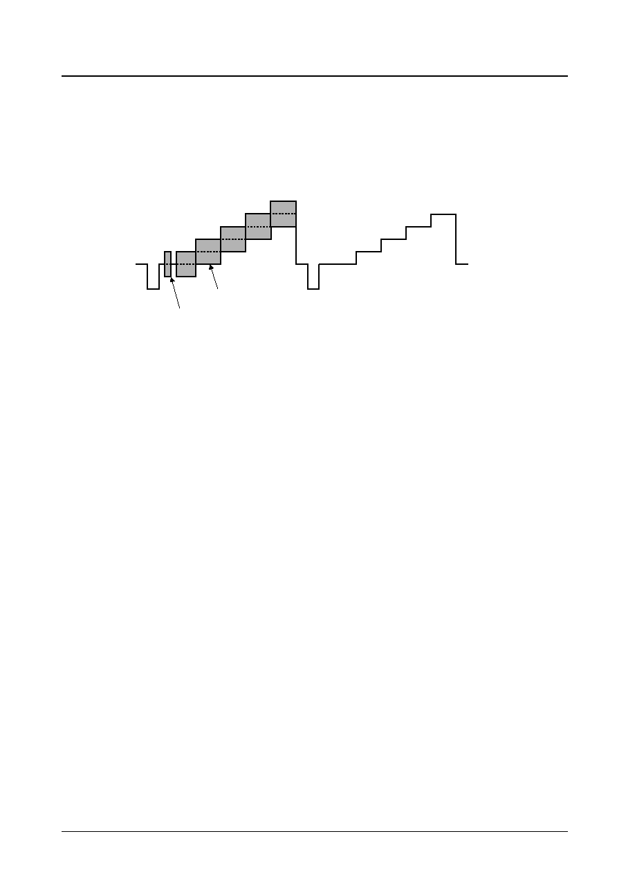
Deflection Block - Input Signals and Test Conditions
For each of the test items, set up the following conditions unless otherwise specified.
1. VIF and SIF blocks: No signal
2. Luminance (Y) input and chrominance (C) input: No signal
3. Sync input: Horizontal/vertical composite sync signal (DC offset: 3.8 V, 40 IRE. Other timing and other parameters
must conform to the FCC broadcast standards.)
Caution: There must be no burst or chrominance signal under the pedestal level.
4. Bus control conditions: All conditions set to their initial values, unless otherwise specified.
5. The delay time from the rise of the horizontal output (the pin 26 output) to the rise of the F.B.P IN (pin 27 input)
must be 9 µs.
6. The pin 18 (the vertical size correction circuit input pin) voltage must be V
CC
(7.6 V).
7. Pin 28 (the x-ray protection circuit input pin) must be connected to ground.
Notes:
Perform the following operations if the horizontal output pulse signal was stopped.
1. Set the bus on/off bit to off (0) temporarily, and then set it to on (1) again.
(If the x-ray protection circuit and/or the PON-RES circuit operate, an IC internal latch circuit will be set. The on/off
bit must be set to off (0) to reset that latch circuit, even if the horizontal output signal is not output. Since the PON-
RES circuit operates when the horizontal supply voltage rises, the on/off bit must be set to off (0).)
2. Note on video muting
If the horizontal output pulse signal was stopped, after performing the operation described in paragraph 1 above, clear
the video muting bit to 0.
(This is because the video muting bit is forcibly set to 1 when the on/off bit is set to 0 or when either the x-ray
protection circuit or the PON-RES circuit operate. This also applies at power on.)
No. 5841-28/39
LA7615
A10074
Signal inappropriate for use as a sync input
Chrominance signal
Signal appropriate for use as a sync input
Burst signal
No. 5841-29/39
LA7615
Parameter
Symbol
Test point
Input signal
Test procedure
Bus condition
[Deflection Block]
Sync separator circuit sensitivity
Horizontal free-running
frequency deviation
Horizontal pull-in range
Horizontal output pulse width @0
Horizontal output pulse width @1
Horizontal output pulse width @2
Horizontal output pulse width @3
Horizontal output pulse
saturation voltage
Horizontal output pulse phase
Ssync
f
H
f
H
PULL
Hduty 0
Hduty 1
Hduty 2
Hduty 3
V
H
sat
HPH
CEN
SYNC IN:
horizontal and
vertical
synchronizing
signal
SYNC IN: no
signal
SYNC IN:
horizontal and
vertical
synchronizing
signal
SYNC IN:
horizontal and
vertical
synchronizing
signal
SYNC IN:
horizontal and
vertical
synchronizing
signal
SYNC IN:
horizontal and
vertical
synchronizing
signal
SYNC IN:
horizontal and
vertical
synchronizing
signal
SYNC IN:
horizontal and
vertical
synchronizing
signal
SYNC IN:
horizontal and
vertical
synchronizing
signal
Gradually decrease the level of the synchronizing
signal input to SYNC IN (pin 44) and measure the
level of the synchronizing signal when the
synchronization is unlocked.
Connect the pin 26 output (Hout) to a frequency
counter and measure the horizontal free-running
frequency.
Calculate the following formula.
f
H
= <measured value> ≠ 15.743 kHz
Monitor the horizontal synchronizing signal input to
SYNC IN (pin 44) and the pin 26 output (Hout) with
an oscilloscope. Vary the frequency of the horizontal
synchronizing signal and measure the pull-in range.
Measure the low-level period in the pin 26 horizontal
pulse waveform.
Measure the low-level period in the pin 26 horizontal
pulse waveform.
Measure the low-level period in the pin 26 horizontal
pulse waveform.
Measure the low-level period in the pin 26 horizontal
pulse waveform.
Measure the voltage during low-level period in the
pin 26 horizontal pulse waveform.
Measure the delay time from the rise of the pin 26
horizontal output pulse waveform to the fall of the
SYNC IN horizontal synchronizing signal.
HDUTY: 00
HDUTY: 01
HDUTY: 11
44
26
44
26
26
26
26
26
26
44
HPHCEN
20 IRE
3.8V
A10075
Horizontal output
Continued on next page.
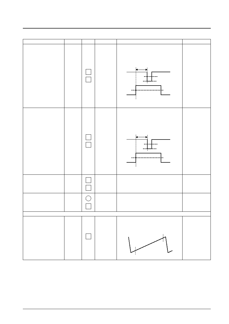
No. 5841-30/39
LA7615
Continued from preceding page.
Parameter
Symbol
Test point
Input signal
Test procedure
Bus condition
Horizontal position adjustment
range
Maximum horizontal position
adjustment variability
X-ray protection circuit operating
voltage
POR circuit operating voltage
[Vertical Screen Size Adjustment]
Vertical ramp output amplitude
@64
HPHrange
HPHstep
VX
RAY
V
POR
Vsize64
SYNC IN:
horizontal and
vertical
synchronizing
signal
SYNC IN:
horizontal and
vertical
synchronizing
signal
SYNC IN:
horizontal and
vertical
synchronizing
signal
SYNC IN:
horizontal and
vertical
synchronizing
signal
SYNC IN:
horizontal and
vertical
synchronizing
signal
Measure the delay time from the rise of the pin 26
horizontal output pulse to the fall of SYNC IN
horizontal synchronizing signal with H
PHASE
set to
both 0 and 15 and calculate the difference with
respect to HPH
CEN
.
Measure the delay time from the rise of the pin 26
horizontal output pulse to the fall of SYNC IN
horizontal synchronizing signal while varying H
PHASE
from 0 to 15, and measure the amount of variation at
each step. Find the step with the largest value of the
data.
Connect a DC voltage source to pin 28, and
gradually increase that voltage starting at 0 V.
Measure the pin 28 DC voltage at the point the pin
26 horizontal output pulse stops.
Replace the current source connected to pin 24 with
a DC voltage source, and gradually decrease the
voltage starting at 7.3 V. Measure the pin 24 DC
voltage at the point the pin 26 horizontal output pulse
stops.
Monitor the pin 19 vertical ramp output and measure
the voltages at the 22nd line and at the 262nd line.
Calculate the following formula.
Vsize64 = Vline262 ≠ Vline22
H
PHASE
: 0000
H
PHASE
: 1111
H
PHASE
: 0000
to
H
PHASE
: 1111
26
44
26
44
26
28
26
19
20 IRE
3.8V
A10076
Measurement
20 IRE
A10077
A10078
262nd line
24
Continued on next page.
Horizontal output
Measurement
Horizontal output
22nd line
Vertical ramp output
No. 5841-31/39
LA7615
Continued from preceding page.
Parameter
Symbol
Test point
Input signal
Test procedure
Bus condition
Vertical ramp output amplitude
@0
Vertical ramp output amplitude
@127
Vertical size correction @7
(maximum)
Vertical ramp DC voltage @32
Vertical ramp DC voltage @0
Vsize0
Vsize127
Vsizecomp
Vdc32
Vdc0
SYNC IN:
horizontal and
vertical
synchronizing
signal
SYNC IN:
horizontal and
vertical
synchronizing
signal
SYNC IN:
horizontal and
vertical
synchronizing
signal
SYNC IN:
horizontal and
vertical
synchronizing
signal
SYNC IN:
horizontal and
vertical
synchronizing
signal
Monitor the pin 19 vertical ramp output and measure
the voltages at the 22nd line and at the 262nd line.
Calculate the following formula.
Vsize0 = Vline262 ≠ Vline22
Monitor the pin 19 vertical ramp output and measure
the voltages at the 22nd line and at the 262nd line.
Calculate the following formula.
Vsize0 = Vline262 ≠ Vline22
Monitor the pin 19 vertical ramp output and measure
the voltages at the 22nd line and at the 262nd line.
Calculate Va from the following formula.
Va = Vline262 ≠ Vline22
Next, apply 3.8 V to pin 18, and once again measure
the voltages at the 22nd line and at the 262nd line.
Calculate Vb from the following formula.
Vb = Vline262 ≠ Vline22
Finally, calculate Vsizecomp from the following
formula.
Vsizecomp = (Va ≠ Vb)/Va
◊
100
Monitor the pin 19 vertical ramp output and measure
the voltage at the 142nd line.
Monitor the pin 19 vertical ramp output and measure
the voltage at the 142nd line.
V
SIZE
: 0000000
V
SIZE
: 1111111
V
COMP
: 111
V
DC
: 000000
19
19
19
19
19
A10079
A10080
A10081
A10082
[High-Voltage Dependency Vertical Size Correction]
[Vertical Screen Position Adjustment]
Continued on next page.
262nd line
22nd line
Vertical ramp output
262nd line
22nd line
Vertical ramp output
142nd line
Vertical ramp output
Vertical ramp output
142nd line
No. 5841-32/39
LA7615
Continued from preceding page.
Parameter
Symbol
Test point
Input signal
Test procedure
Bus condition
Vertical ramp DC voltage @63
Vertical linearity @8
Vertical linearity @0
Vertical linearity @15
Vdc63
Vlin8
Vlin0
Vlin15
SYNC IN:
horizontal and
vertical
synchronizing
signal
SYNC IN:
horizontal and
vertical
synchronizing
signal
SYNC IN:
horizontal and
vertical
synchronizing
signal
SYNC IN:
horizontal and
vertical
synchronizing
signal
Monitor the pin 19 vertical ramp output and measure
the voltage at the 142nd line.
Monitor the pin 19 vertical ramp output and measure
the voltages at the 22nd line, the 142nd line, and the
262nd line. Let Va, Vb, and Vc be these
measurements, and calculate the following formula.
Vline8 = (Vb ≠ Va)/(Vc ≠ Va)
Monitor the pin 19 vertical ramp output and measure
the voltages at the 22nd line, the 142nd line, and the
262nd line. Let Va, Vb, and Vc be these
measurements, and calculate the following formula.
Vline0 = (Vb ≠ Va)/(Vc ≠ Va)
Monitor the pin 19 vertical ramp output and measure
the voltages at the 22nd line, the 142nd line, and the
262nd line. Let Va, Vb, and Vc be these
measurements, and calculate the following formula.
Vline15 = (Vb ≠ Va)/(Vc ≠ Va)
V
DC
: 111111
VLIN: 0000
VLIN: 1111
19
19
19
19
A10083
A10084
A10085
A10086
Continued on next page.
Vertical ramp output
142nd line
Vertical ramp output
142nd line
262nd line
22nd line
Vertical ramp output
142nd line
262nd line
22nd line
Vertical ramp output
142nd line
262nd line
22nd line
No. 5841-33/39
LA7615
Continued from preceding page.
Parameter
Symbol
Test point
Input signal
Test procedure
Bus condition
Vertical S-curve correction @8
Vertical S-curve correction @0
Vertical S-curve correction @15
VScor8
VScor0
VScor15
SYNC IN:
horizontal and
vertical
synchronizing
signal
SYNC IN:
horizontal and
vertical
synchronizing
signal
SYNC IN:
horizontal and
vertical
synchronizing
signal
Monitor the pin 19 vertical ramp output and measure
the voltages at the 32nd line, the 52nd line, the
132nd line, the 152nd line, the 232nd line, and the
252nd line. Let Va, Vb, Vc, Vd, Ve, and Vf be these
measurements, and calculate the following formula.
VScor8 = 0.5[(Vb ≠ Va) + (Vf ≠ Ve)] / (Vd ≠ Vc)
Monitor the pin 19 vertical ramp output and measure
the voltages at the 32nd line, the 52nd line, the
132nd line, the 152nd line, the 232nd line, and the
252nd line. Let Va, Vb, Vc, Vd, Ve, and Vf be these
measurements, and calculate the following formula.
VScor0 = 0.5[(Vb ≠ Va) + (Vf ≠ Ve)] / (Vd ≠ Vc)
Monitor the pin 19 vertical ramp output and measure
the voltages at the 32nd line, the 52nd line, the
132nd line, the 152nd line, the 232nd line, and the
252nd line. Let Va, Vb, Vc, Vd, Ve, and Vf be these
measurements, and calculate the following formula.
VScor15 = 0.5[(Vb ≠ Va) + (Vf ≠ Ve)] / (Vd ≠ Vc)
VS: 1000
VS: 1111
19
19
19
A10087
A10088
A10089
Continued on next page.
Vertical ramp output
252nd line
232nd line
152nd line
132nd line
52nd line
32nd line
Vertical ramp output
252nd line
232nd line
152nd line
132nd line
52nd line
32nd line
Vertical ramp output
252nd line
232nd line
152nd line
132nd line
52nd line
32nd line
No. 5841-34/39
LA7615
Parameter
Symbol
Test point
Input signal
Test procedure
Bus condition
[Horizontal Size Adjustment]
East/west DC voltage @16
East/west DC voltage @0
East/west DC voltage @31
East/west parabola amplitude
@8
East/west parabola amplitude
@0
EWdc16
EWdc0
EWdc31
EWamp8
EWamp0
SYNC IN:
horizontal and
vertical
synchronizing
signal
SYNC IN:
horizontal and
vertical
synchronizing
signal
SYNC IN:
horizontal and
vertical
synchronizing
signal
SYNC IN:
horizontal and
vertical
synchronizing
signal
SYNC IN:
horizontal and
vertical
synchronizing
signal
Monitor the pin 21 east/west output (parabola
waveform output) and measure the voltage at the
142nd line.
Monitor the pin 21 east/west output (parabola
waveform output) and measure the voltage at the
142nd line.
Monitor the pin 21 east/west output (parabola
waveform output) and measure the voltage at the
142nd line.
Monitor the pin 21 east/west output (parabola
waveform output) and measure the voltages at the
22nd line and at the 142nd line. Let Va and Vb be
these measurements, and calculate the following
formula.
EWamp8 = Vb ≠ Va
Monitor the pin 21 east/west output (parabola
waveform output) and measure the voltages at the
22nd line and at the 142nd line. Let Va and Vb be
these measurements, and calculate the following
formula.
EWamp0 = Vb ≠ Va
EW
DC
: 00000
EW
DC
: 11111
EW
AMP
: 0000
21
21
21
21
21
A10090
East/west output
A10091
A10092
A10093
A10094
[Pin-Cushion Distortion Correction]
Continued on next page.
142nd line
East/west output
142nd line
East/west output
142nd line
East/west output
142nd line
22nd line
East/west output
142nd line
22nd line
No. 5841-35/39
LA7615
Continued from preceding page.
Parameter
Symbol
Test point
Input signal
Test procedure
Bus condition
East/west parabola amplitude
@15
East/west parabola tilt @8
East/west parabola tilt @0
East/west parabola tilt @15
EWamp15
EWtilt8
EWtilt0
EWtilt15
SYNC IN:
horizontal and
vertical
synchronizing
signal
SYNC IN:
horizontal and
vertical
synchronizing
signal
SYNC IN:
horizontal and
vertical
synchronizing
signal
SYNC IN:
horizontal and
vertical
synchronizing
signal
Monitor the pin 21 east/west output (parabola
waveform output) and measure the voltages at the
22nd line and at the 142nd line. Let Va and Vb be
these measurements, and calculate the following
formula.
EWamp15 = Vb ≠ Va
Monitor the pin 21 east/west output (parabola
waveform output) and measure the voltages at the
22nd line and at the 262nd line. Let Va and Vb be
these measurements, and calculate the following
formula.
EWamp8 = Va ≠ Vb
Monitor the pin 21 east/west output (parabola
waveform output) and measure the voltages at the
22nd line and at the 262nd line. Let Va and Vb be
these measurements, and calculate the following
formula.
EWtilt0 = Va ≠ Vb
Monitor the pin 21 east/west output (parabola
waveform output) and measure the voltages at the
22nd line and at the 262nd line. Let Va and Vb be
these measurements, and calculate the following
formula.
EWtilt15 = Va ≠ Vb
EW
AMP
: 1111
EW
TILT
: 0000
EW
TILT
: 1111
21
21
21
21
A10095
A10096
A10097
A10098
[Trapezoidal Distortion Correction]
Continued on next page.
East/west output
142nd line
22nd line
East/west output
262nd line
22nd line
East/west output
262nd line
22nd line
East/west output
262nd line
22nd line
No. 5841-36/39
LA7615
Continued from preceding page.
Parameter
Symbol
Test point
Input signal
Test procedure
Bus condition
[Corner Distortion Correction]
East/west parabola corner: Top
East/west parabola corner:
Bottom
[Sandcastle Output]
Burst gate pulse peak value
Burst gate pulse phase
Burst gate pulse width
EWcortop
EWcorbot
V
BGP
Td
BGP
PW
BGP
SYNC IN:
horizontal and
vertical
synchronizing
signal
SYNC IN:
horizontal and
vertical
synchronizing
signal
SYNC IN:
horizontal and
vertical
synchronizing
signal
SYNC IN:
horizontal and
vertical
synchronizing
signal
SYNC IN:
horizontal and
vertical
synchronizing
signal
Monitor the pin 21 east/west output (parabola
waveform output) and measure the voltage at the
22nd line under the conditions with COR
TOP
set to
111 and to 000. Let Va and Vb be these
measurements. Calculate the following formula.
EWcortop = Va ≠ Vb
Monitor the pin 21 east/west output (parabola
waveform output) and measure the voltage at the
262nd line under the conditions with COR
BOT
set to
111 and to 000. Let Va and Vb be these
measurements. Calculate the following formula.
EWcorbot = Va ≠ Vb
Measure the pin 29 output burst gate pulse peak
value.
Measure the delay time from the rise of the
horizontal synchronizing signal to the rise of the pin
29 burst gate pulse.
Measure the width of the pin 29 burst gate pulse.
CORT
OP
: 111-000
CORBOTTOM:
111-000
21
21
29
29
44
29
A10099
A10100
VBGP
BGP
A10101
Pin 29 output
TdBGP
BGP
A10102
Horizontal synchronizing signal
PWBGP
BGP
A10103
Continued on next page.
East/west output
22nd line
East/west output
262nd line
Pin 29 output
Pin 29 output
No. 5841-37/39
LA7615
Continued from preceding page.
Parameter
Symbol
Test point
Input signal
Test procedure
Bus condition
Blanking pulse peak value
[D/A Converter Output]
Pin 30 D/A converter output
voltage @0
Pin 30 D/A converter output
voltage @8
Pin 30 D/A converter output
voltage @15
V
BLK
V
DAC
0
V
DAC
8
V
DAC
15
SYNC IN:
horizontal and
vertical
synchronizing
signal
Measure the peak value of the pin 29 output
blanking pulse.
Measure the pin 30 D/A converter output DC
voltage.
Measure the pin 30 D/A converter output DC
voltage.
Measure the pin 30 D/A converter output DC
voltage.
+B
TRIM
: 0000
+B
TRIM
: 1111
29
30
30
30
VBLK
A10104
Blanking pulse
Pin 29 output
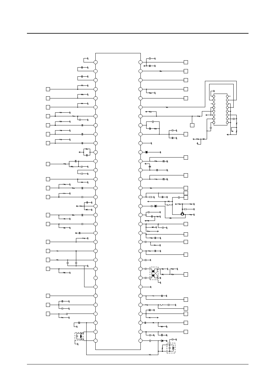
No. 5841-38/39
LA7615
Test Circuit Diagram
1
FM
DISCRI
2
IF
V
CC
3
AUX
VIDEO
IN
4
RF
AGC
OUT
5
WB
AUDIO
OUT
6
PIF
APC
FILTER
7
IF
GND
8
PIF
IN1
VIF
IN
9
PIF
IN2
10
PIF
AGC1
11
PIF
AGC2
12
SIF
IN
13
SIF
AGC
14
AFT
OUT
15
CHROMA
APC
16
XTAL
17
VERT
V
CC
18
SIZE
COMP
19
VERT
OUT
20
RAMP
ALC
FILTER
21
E-W
OUT
22
HORIZ
RES
23
HORIZ
GND
24
STANDBY
V
CC
25
HORIZ
AFC
FILTER
26
HORIZ
OUT
39
38
37
36
35
34
33
FAST
SWITCH
IN
40
RED
IN
41
GRN
IN
42
BLU
IN
43
BLACK
LEVEL
DET
44
SYNC
IN
45
ADAPTIVE
CORING
46
SELECTED
Y
OUT
47
Y2
IN
48
C2
IN
49
CHROMA
KILLER
50
Y1
IN
51
C1
IN
52
TEST
IT
FILTER
53
SELECTED
VIDEO
OUT
54
BUS
CLOCK
55
BUS
DATA
56
VIDEO
OUT
57
EQ
FILTER
58
BUS
GND
59
SND
IF
OUT
60
FM
V
CC
61
SND
IF
IN
62
F0
FILTER
63
VCO
TANK2
64
VCO
TANK1
+
+
+
+
+
+
+
+
+
+
+
+
+
+
+
+
+
3
4
5
6
2
+
9
13
16
17
18
19
24
26
28
36
11
12
14
+
21
30
31
27
FLYBACK
BLU
OUT
+
32
29
28
X
RAY
GRN
OUT
29
SAND
CASTLE
OUT
RED
OUT
30
DAC
OUT
BRT
ABL
FILT
31
IB
IN
CONTRAST
(PIX)
ABL
FILT
+
32
VID
CHROMA
V
CC
VID/
CHROMA
GND
4
3
5
6
7
8
2
1
13
14
12
11
10
9
15
16
LC4528B
37
38
53
+
40
+
41
+
42
46
+
47
48
54
55
+
50
51
44
39
56
60
59
61
+
+
LA7615
A10105
R75
R76
3.9 k
1744
C118
C2
C1
C7
C6
C4
C8
C9
C3
C119
R1
R2
R5
R3
R7
R4
75
100
50 k
150
16
R10
820
R11
50
R12
R13
100 k
R16
3 k
R18
R26
6.2 k
1 k
3.3 k
10 k
10 k
1.8 k
16 pF
R15
R25
R27
R28
R36
CSB503F (44)
750
CHR1
R22
7.5 k
R17
C16
C117
C21
C23
C24
C26
C27
C29
R40
R42
R43
C34
C35
R41
C31
C28
C22
0.01
µ
F
0.01
µ
F
100
µ
F
10
µ
F
0.47
µ
F
10
µ
F
10
µ
F
1
µ
F
C36
C37
R46
R47
R48
R49
R51
R52
R53
R50
16 k
16 k
16 k
75
75
75
75
1100
1.5
µ
F
C39
C40
C41
C42
C44
R57
R56
560
C43
470 k
1
µ
F
C50
C45
C46
C47
C48
C49
C51
C55
C56
C58
C59
R74
50
R67
2.2
µ
F
1
µ
F
100 pF
10
µ
F
1
µ
F
0.01
µ
F
0.01
µ
F
1
µ
F
R60
R59
R61
R62
R62
R63
R64
R65
R68
R69
R70
R58
0.01
µ
F
1
µ
F
100 pF
100
75
75
15 k
2 k
15 k
100
75
75
100
100
24 k
100 pF
10 k
R54
680 k
22
µ
F
C38
1
µ
F
1
µ
F
1
µ
F
47 pF
1
µ
F
0.01
µ
F
0.033
µ
F
2.2 k
10 k
100
µ
F
0.01
µ
F
1 k
1 k
0.01
µ
F
470
R21
1.6 k
R14
100 k
R9
50
R8
68
R6
16
IF1
7.5 k
1T363
0.01
µ
F
0.01
µ
F
1
µ
F
0.01
µ
F
0.47
µ
F
0.01
µ
F
0.01
µ
F
C10
0.022
µ
F
C12
0.01
µ
F
C11
0.047
µ
F
C13
1
µ
F
C14
0.01
µ
F
C15
C17
C19
10
µ
F
0.033
µ
F
100
µ
F
1
µ
F
0.01
µ
F
100 k
+9 V
T101
M
+7.6 V
+7.6 V
+9 V
C25
+7.6 V
0.47
µ
F
*
+9 V
Tr1
V101
766-2
+7.6 V
+7.6 V
+7.6 V
R33
C22
R38
5 k
2200 pF
1 k
R32
8.2 k
C30
1500 pF
+7.6 V
NC
NC
R37
R34
8.2 k
5 k
+7.6 V
WIDTH (12US)
DELAY2
(9US)
+7.6 V
+7.6 V
+
7.6 V
C53
C52
100 pF
100 pF
L102
M
*
: Used for adjusting the characteristics of the crystal oscillator.
(Includes two monostable multivibrators.)
PS No. 5841-39/39
LA7615
This catalog provides information as of September, 1999. Specifications and information herein are
subject to change without notice.
Specifications of any and all SANYO products described or contained herein stipulate the performance,
characteristics, and functions of the described products in the independent state, and are not guarantees
of the performance, characteristics, and functions of the described products as mounted in the customer's
products or equipment. To verify symptoms and states that cannot be evaluated in an independent device,
the customer should always evaluate and test devices mounted in the customer's products or equipment.
SANYO Electric Co., Ltd. strives to supply high-quality high-reliability products. However, any and all
semiconductor products fail with some probability. It is possible that these probabilistic failures could
give rise to accidents or events that could endanger human lives, that could give rise to smoke or fire,
or that could cause damage to other property. When designing equipment, adopt safety measures so
that these kinds of accidents or events cannot occur. Such measures include but are not limited to protective
circuits and error prevention circuits for safe design, redundant design, and structural design.
In the event that any or all SANYO products (including technical data, services) described or contained
herein are controlled under any of applicable local export control laws and regulations, such products must
not be exported without obtaining the export license from the authorities concerned in accordance with the
above law.
No part of this publication may be reproduced or transmitted in any form or by any means, electronic or
mechanical, including photocopying and recording, or any information storage or retrieval system,
or otherwise, without the prior written permission of SANYO Electric Co., Ltd.
Any and all information described or contained herein are subject to change without notice due to
product/technology improvement, etc. When designing equipment, refer to the "Delivery Specification"
for the SANYO product that you intend to use.
Information (including circuit diagrams and circuit parameters) herein is for example only; it is not
guaranteed for volume production. SANYO believes information herein is accurate and reliable, but
no guarantees are made or implied regarding its use or any infringements of intellectual property rights
or other rights of third parties.