 | –≠–ª–µ–∫—Ç—Ä–æ–Ω–Ω—ã–π –∫–æ–º–ø–æ–Ω–µ–Ω—Ç: LA7642N | –°–∫–∞—á–∞—Ç—å:  PDF PDF  ZIP ZIP |
Overview
The LA7642N integrates the chrominance circuit for a
SECAM format TV in a single 16-pin DIP (300 mil)
package and provides an adjustment-free discriminator
circuit. In combination with the Sanyo LA7687, LA7688,
this IC can implement a multi-format color TV signal-
processing system.
Features
∑ Adjustment-free discriminator circuit
∑ On-chip bell filter
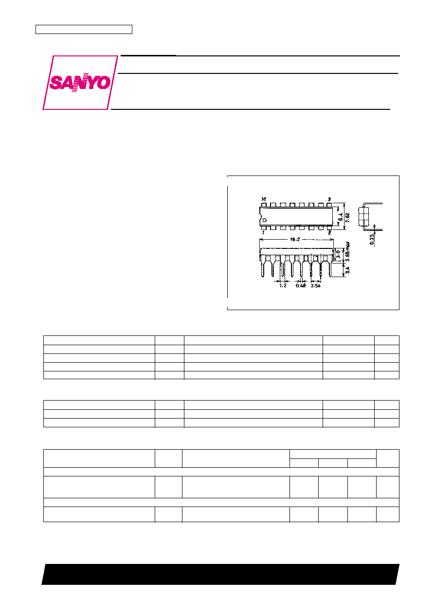
Package Dimensions
unit: mm
3006B-DIP16
Monolithic Linear IC
Ordering number : EN5693
73097HA(OT) No. 5693-1/6
SANYO: DIP16
[LA7642N]
SANYO Electric Co.,Ltd. Semiconductor Bussiness Headquarters
TOKYO OFFICE Tokyo Bldg., 1-10, 1 Chome, Ueno, Taito-ku, TOKYO, 110 JAPAN
SECAM Format Color TV Chrominance Circuit
LA7642N
Parameter
Symbol
Conditions
Ratings
Unit
Maximum supply voltage
V
CC
max
9
V
Allowable power dissipation
Pd max
Ta
65∞C
400
mW
Operating temperature
Topr
≠10 to +65
∞C
Storage temperature
Tstg
≠55 to +125
∞C
Specifications
Maximum Ratings
at Ta = 25∞C
Parameter
Symbol
Conditions
Ratings
Unit
Recommended operating voltage
V
CC
7.8
V
Operating voltage range
V
CC
op
7.0 to 8.5
V
Operating Conditions
at Ta = 25∞C
Parameter
Symbol
Conditions
Ratings
Unit
min
typ
max
[Circuit Voltage and Current]
Chrominance system. Measure the current
Circuit current
I
CC
flowing into pin 15; With no signal applied to
28
35
42
mA
pin 14.
[Filter Block]
Input impedance
The pin 14 input impedance. For reference
15
k
only (design value)
Operating Characteristics
at Ta = 25∞C, V
CC
= 7.8 V, with pin 13 pulled up to V
CC
through a 20-k
resistor
Continued on next page.
No. 5693-2/6
LA7642N
Parameter
Symbol
Conditions
Ratings
Unit
min
typ
max
Referenced to 4.286 MHz. For reference only.
EQU = off.
Input a 20 mV p-p, f = 4.286 MHz CW signal
Bell filter frequency characteristics
BEL4.086
to pin 14 and, measure the pin 16 output
≠9
≠6
≠3
dB
4.086 MHz
(f = 4.286 MHz). Next, input a CW of
20 mV p-p, f = 4.086 MHz and measure the
pin 16 output (f = 4.086 MHz) and calculate
the frequency characteristics.
Referenced to 4.286 MHz. For reference only.
EQU = off.
Input a 20 mV p-p, f = 4.286 MHz CW signal
Bell filter frequency characteristics
BEL4.486
to pin 14 and, measure the pin 16 output
≠5
≠2
≠0.5
dB
4.486 MHz
(f = 4.286 MHz). Next, input a CW of
20 mV p-p, f = 4.486 MHz and measure the
pin 16 output (f = 4.486 MHz) and calculate
the frequency characteristics.
Referenced to 4.286 MHz. For reference only.
EQU = on.
Input a 20 mV p-p, f = 4.286 MHz CW signal
EQU frequency characteristics
EQU4.086
to pin 14 and, measure the pin 16 output
≠10.5
≠7.5
≠4.5
dB
4.086 MHz
(f = 4.286 MHz). Next, input a CW of
20 mV p-p, f = 4.086 MHz and measure the
pin 16 output (f = 4.086 MHz) and calculate
the frequency characteristics.
Referenced to 4.286 MHz. For reference only.
EQU = on.
Input a 20 mV p-p, f = 4.286 MHz CW signal
EQU frequency characteristics
EQU4.486
to pin 14 and measure the pin 16 output
≠3
0
+3
dB
4.486 MHz
(f = 4.286 MHz). Next, input a CW of
20 mV p-p, f = 4.486 MHz and measure the
pin 16 output (f = 4.486 MHz) and calculate
the frequency characteristics.
Referenced to 4.35 MHz. For reference only.
EQU = off.
Input a 20 mV p-p CW signal to pin 14 and
Bell filter frequency deviation from
BELF0
modify the frequency of that signal. Measure
≠50
0
+50
kHz
center frequency
the deviation from 4.35 MHz of the frequency
(the center frequency) for which the pin 16
output is maximized.
Referenced to 4.35 MHz. For reference only.
Bell filter gain difference at f0 ±500 kHz
BELdG
EQU = off.
≠1
0
+1
dB
Measure the gain at the BELF0 ±500 kHz,
and calculate the difference.
[Chrominance Block]
Let 0 dB = 200 mV p-p. Input a color bar
signal to pin 14 and gradually lower the input
Killer operating point
KILL
signal level. Measure the input level at the
≠42
≠36
≠33
dB
point the pin 13 DC voltage falls below 1/2
*
V
CC
.
The pin 7 B-Y amplitude for a color bar signal.
B-Y output amplitude
VBY
Let 0 dB = 200 mV p-p. Input a color bar
0.60
0.75
0.90
Vp-p
signal (0 dB) to pin 14, and measure the B-Y
amplitude at pin 7.
The pin 6 R-Y amplitude for a color bar signal.
R-Y output amplitude
VRY
Let 0 dB = 200 mV p-p. Input a color bar
0.74
0.92
1.10
Vp-p
signal (0 dB) to pin 14, and measure the R-Y
amplitude at pin 6.
VRY/VBY. Calculate the ratio of the values
R-Y/B-Y output ratio
RATRB
measured above.
1.1
1.23
1.35
RATRB = VRY/VBY
Input a color bar signal (0 dB) to pin 14. In the
pin 7 (B-Y) output waveform measure the
amplitude of the blue (+230 kHz) and yellow
B-Y linearity
LINBY
(≠230 kHz) components (A) and measure the
85
100
115
%
amplitude of the blue green (+78 kHz) and
red (≠78 kHz) components (B). Calculate the
value of LINBY from the following formula.
LINBY = (A/B)
◊
(156/460)
◊
100 (%)
Continued from preceding page.
Continued on next page.
No. 5693-3/6
LA7642N
Parameter
Symbol
Conditions
Ratings
Unit
min
typ
max
Input a color bar signal (0 dB) to pin 14. In the
pin 6 (R-Y) output waveform measure the
amplitude of the blue green (+280 kHz) and
R-Y linearity
LINRY
red (≠280 kHz) components (A) and measure
85
100
115
%
the amplitude of the blue (+45 kHz) and
yellow (≠45 kHz) components (B). Calculate
the value of LINRY from the following formula.
LINRY = (A/B)
◊
(90/560)
◊
100 (%)
Measure the peak value of the pin 7 ALC
ALC pulse height
VALC
pulse signal.
180
200
220
mVp-p
Referenced to the blanking period DC level.
Blanking period B-Y DC voltage
VALC
The pin 7 blanking period DC level.
3.8
4.1
4.4
V
Blanking period R-Y DC voltage
VRYBLK
The pin 6 blanking period DC level.
3.8
4.1
4.4
V
The pin 7 output impedance. For reference
only.
Input a color bar signal (0 dB) to pin 14 and
measure the pin 7 B-Y amplitude Vb (V p-p).
SECAM output impedance: B-Y
ZBYS
Next, connect a 2-k
resistor between pin 7
150
and ground and measure the pin 7 B-Y
amplitude Vwrb (V p-p). Derive ZBYS from
the following formula.
ZBYS = (Vb ≠ Vwrb)/Vwrb
◊
2k (
).
The pin 6 output impedance. For reference
only.
Input a color bar signal (0 dB) to pin 14 and
measure the pin 6 R-Y amplitude Vr (V p-p).
SECAM output impedance: R-Y
ZRYS
Next, connect a 2-k
resistor between pin 6
150
and ground and measure the pin 6 R-Y
amplitude Vwrr (V p-p). Derive ZRYS from
the following formula.
ZRYS = (Vr ≠ Vwrr)/Vwrr
◊
2k (
).
The pin 7 output impedance. For reference
Output impedance
only.
Non-SECAM: B-Y
ZBY
Apply a 4-V signal to pin 7 (B-Y), measure
10
M
the influx current Ib, and derive ZBY from the
following formula. ZBY = 4/Ib (M
)
The pin 6 output impedance. For reference
Output impedance
only.
Non-SECAM: R-Y
ZRY
Apply a 4-V signal to pin 6 (R-Y), measure
10
M
the influx current Ir, and derive ZRY from the
following formula. ZRY = 4/Ir (M
)
The DC difference between the pin 7 no
signal period DC level and the signal period
Black level error B-Y
BBBY
DC level for a black-and-white signal.
≠5
0
+5
kHz
Measure DBY (V) and calculate BBBY from
the following formula.
BBBY = DBY
◊
460/VBY kHz
The DC difference between the pin 6 no
signal period DC level and the signal period
Black level error R-Y
BBRY
DC level for a black-and-white signal.
≠5
0
+5
kHz
Measure DRY (V) and calculate BBRY from
the following formula.
BBRY = DRY
◊
460/VRY kHz
[De-Emphasis Characteristics]
Input a signal to which a 63-kHz modulation
has been applied to pin 14 and measure the
pin 7 B-Y amplitude Vbon (V p-p) when
De-emphasis 63k B-Y
DE63B
preemphasis is on. Next, turn off pre-
≠1.0
≠2.6
≠4.0
dB
emphasis, measure the pin 7 B-Y amplitude
Vboff (V p-p), and calculate DE63B from the
following formula.
DE63B = 20
◊
log (Vboff/Vbon) (dB)
Continued from preceding page.
Continued on next page.
No. 5693-4/6
LA7642N
Parameter
Symbol
Conditions
Ratings
Unit
min
typ
max
Input a signal to which a 63-kHz modulation
has been applied to pin 14 and measure the
pin 6 R-Y amplitude Vron (V p-p) when pre-
De-emphasis 63k R-Y
DE63R
emphasis is on. Next, turn off preemphasis,
≠1.0
≠2.6
≠4.0
dB
measure the pin 6 R-Y amplitude Vroff
(V p-p), and calculate DE63R from the
following formula.
DE63R = 20
◊
log (Vroff/Vron) (dB)
Input a signal to which a 250-kHz modulation
has been applied to pin 14 and measure the
pin 7 B-Y amplitude Vbon (V p-p) when pre-
De-emphasis 250k B-Y
DE250B
emphasis is on. Next, turn off preemphasis,
≠4.5
≠7.0
≠9.5
dB
measure the pin 7 B-Y amplitude Vboff
(V p-p), and calculate DE250B from the
following formula.
DE250B = 20
◊
log (Vboff/Vbon) (dB)
Input a signal to which a 250-kHz modulation
has been applied to pin 14 and measure the
pin 6 R-Y amplitude Vron (V p-p) when pre-
De-emphasis 250k R-Y
DE250R
emphasis is on. Next, turn off preemphasis,
≠6.5
≠9.0
≠11.5
dB
measure the pin 6 R-Y amplitude Vroff
(V p-p), and calculate DE250R from the
following formula.
DE250R = 20
◊
log (Vroff/Vron) (dB)
[Sandcastle Pulse]
Apply at least 16 pulses with an amplitude of
0 V to V
CC
and then take the following
V threshold voltage
VBLK
measurement. Apply a DC voltage to pin 10
1.0
1.3
1.6
V
and slowly increase this voltage starting at
0 V. Measure the DC voltage applied to pin
at the point the pin 3 DC voltage exceeds 3 V.
Apply at least 16 pulses with an amplitude of
0 V to V
CC
and then take the following
measurement. Apply a pulse signal with a
12-µs high period and a 52-µs low period
H threshold voltage
HBLK
(for a 64-µs cycle) and slowly increase the
2.5
3.0
3.5
V
amplitude of that signal starting at 0. Measure
the wave height of that pulse signal at the
point the pin 7 (B-Y) DC voltage exceeds
VBYBLK + 100 mV.
Apply at least 16 pulses with an amplitude of
0 V to V
CC
and then take the following
measurement. Apply a pulse signal with a
12-µs high period and a 52-µs low period
BGP threshold voltage
BGP
(for a 64-µs cycle) and slowly increase the
4.5
5.0
5.5
V
amplitude of that signal starting at 0. Measure
the wave height of that pulse signal at the
point the pin 4 (IDF) DC voltage becomes
higher than it was at the point the pulse signal
wave height was 0.
[System Switching]
Slowly increase the pin 12 DC voltage from
SECAM threshold voltage 1
SESWLO 0 V and measure that voltage at the point
1.0
1.3
1.6
V
the mode switches to a non-SECAM mode.
Slowly increase the pin 12 DC voltage from
SECAM threshold voltage 2
SESWHI
3 V and measure that voltage at the point
3.6
3.9
4.3
V
the mode switches to SECAM mode.
[Killer Output: Pin 13]
Killer on output level
VKILON
Measure the pin 13 voltage when the killer
0.0
0.2
0.5
V
circuit is on.
Killer off output level
VKILOF
Measure the pin 13 voltage when the killer
7.3
7.8
7.8
V
circuit is off.
[Reference Frequency Input Block]
Measure the variation in the pin 5 DC voltage
4.00-MHz input level variations 1
V5DS4
when the 4.00-MHz input level is changed
≠50
0
+50
mV
from 200 mV p-p to 100 mV p-p.
Continued from preceding page.
No. 5693-5/6
LA7642N
Parameter
Symbol
Conditions
Ratings
Unit
min
typ
max
Measure the variation in the pin 5 DC voltage
4.00-MHz input level variations 2
V5DB4
when the 4.00-MHz input level is changed
≠50
0
+50
mV
from 200 mV p-p to 300 mV p-p.
Measure the variation in the pin 3 DC voltage
4.43-MHz input level variations 1
V3DS44
when the 4.43-MHz input level is changed
≠50
0
+50
mV
from 200 mV p-p to 100 mV p-p.
Measure the variation in the pin 3 DC voltage
4.43-MHz input level variations 2
V3DB44
when the 4.43-MHz input level is changed
≠50
0
+50
mV
from 200 mV p-p to 300 mV p-p.
4.00-MHz input impedance
Z9
The pin 9 input impedance. For reference
15
k
only (design value)
4.43-MHz input impedance
Z11
The pin 11 input impedance. For reference
15
k
only (design value)
[V
CC
Dependency]
The percentage change in the ALC pulse
peak value when V
CC
changes by 1 V.
ALC pulse wave height
dVALC
Measure the ALC pulse peak value when
10
15
20
%
V
CC
= 9 V and record this value as VALC9.
Calculate dVALC from the following formula.
(VALC9 ≠ VALC)/1.2/VALC
◊
100 (%)
Continued from preceding page.
Notes: EQU = off: Pull pin 16 to ground through a 4.7-k
resistor.
EQU = on: Leave pin 16 open.
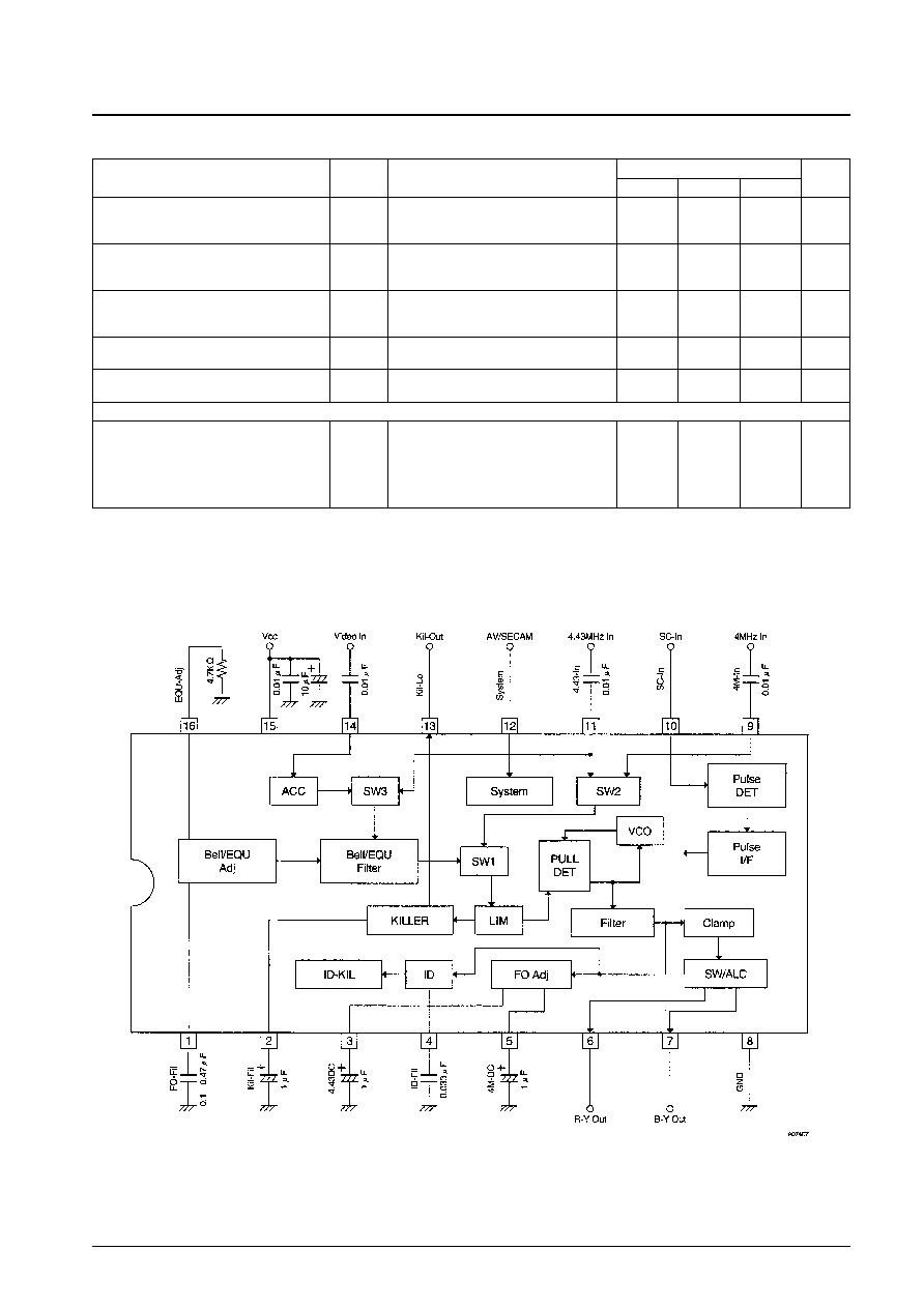
Block Diagram

No. 5693-6/6
LA7642N
This catalog provides information as of July, 1997. Specifications and information herein are subject to change
without notice.
s
No products described or contained herein are intended for use in surgical implants, life-support systems, aerospace
equipment, nuclear power control systems, vehicles, disaster/crime-prevention equipment and the like, the failure of
which may directly or indirectly cause injury, death or property loss.
s
Anyone purchasing any products described or contained herein for an above-mentioned use shall:
Accept full responsibility and indemnify and defend SANYO ELECTRIC CO., LTD., its affiliates, subsidiaries and
distributors and all their officers and employees, jointly and severally, against any and all claims and litigation and all
damages, cost and expenses associated with such use:
Not impose any responsibility for any fault or negligence which may be cited in any such claim or litigation on
SANYO ELECTRIC CO., LTD., its affiliates, subsidiaries and distributors or any of their officers and employees
jointly or severally.
s
Information (including circuit diagrams and circuit parameters) herein is for example only; it is not guaranteed for
volume production. SANYO believes information herein is accurate and reliable, but no guarantees are made or implied
regarding its use or any infringements of intellectual property rights or other rights of third parties.