 | –≠–ª–µ–∫—Ç—Ä–æ–Ω–Ω—ã–π –∫–æ–º–ø–æ–Ω–µ–Ω—Ç: LA7688 | –°–∫–∞—á–∞—Ç—å:  PDF PDF  ZIP ZIP |
Overview
The LA7688 integrates VIF, SIF, video, chrominance, and
deflection processing circuits for PAL/NTSC format TV
sets on a single chip and is provided in a 52-pin shrink
package.
The VIF and SIF circuits achieve semi-adjustment-free
operation, and are adjustment-free except for the VCO coil
and the RF AGC circuit. The chrominance circuit can be
made adjustment-free by using the LC89950 1H delay line
IC. All the signal processing required for a multi-format
color TV can be implemented by combining this product
with the LA7642 SECAM decoder IC.
Features
[VIF]
∑ PLL detector ∑ Buzz canceller
[SIF]
∑ PLL detector ∑ Audio switch
[VIDEO]
∑ Built-in trap ∑ Built-in DL
∑ Aperture control
∑ Video switch (SVO output)
∑ Black expansion
[CHROMA]
∑ PAL/NT ∑ Base band processing
(adjustment free)
∑ Built-in bandpass filter
[OSD]
∑ Analog OSD
[DEF]
∑ Automatic 50/60 Hz discrimination
∑ Fixed vertical size ∑ Double AFC
∑ Built-in sync separator circuit
[Other features] ∑ Sandcastle pulse (for the 1H delay line)
∑ fsc output (for SECAM systems)
∑ Primary color output
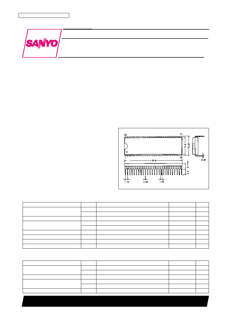
Package Dimensions
unit: mm
3218-DIP52S
Monolithic Linear IC
Ordering number : EN5635
82097HA(OT) No. 5635-1/6
SANYO: DIP52S
[LA7688]
SANYO Electric Co.,Ltd. Semiconductor Bussiness Headquarters
TOKYO OFFICE Tokyo Bldg., 1-10, 1 Chome, Ueno, Taito-ku, TOKYO, 110 JAPAN
Single-Chip CTV Signal-Processing Circuit
for PAL and NTSC Formats
LA7688
Parameter
Symbol
Conditions
Ratings
Unit
Maximum supply voltage
V
40
max
9
V
V
45
max
9
V
Maximum supply current
I
24
max
16
mA
FBP input current
I
26
max
5
mA
I
32
max
10
mA
FBP input voltage
I
26
min
≠5
V
Allowable power dissipation
Pd max
Ta
65∞C When mounted on a printed circuit board
*
1.3
W
Operating temperature
Topr
≠10 to +65
∞C
Storage temperature
Tstg
≠55 to +150
∞C
Specifications
Maximum Ratings
at Ta = 25∞C
Parameter
Symbol
Conditions
Ratings
Unit
Recommended supply voltage
V
40
7.6
V
V
45
7.6
V
Recommended supply current
I24
12
mA
Operating voltage range
V
40
op
7 to 8.2
V
V
45
op
7 to 8.2
V
Operating current range
I
24
op
10 to 16
mA
Operating Conditions
at Ta = 25∞C
Note :
*
Printed circuit board size: 83
◊
86
◊
1.5 mm, material: Bakelite
No. 5635-2/6
LA7688
Parameter
Symbol
Conditions
Ratings
Unit
min
typ
max
[Circuit Voltages and Currents]
Horizontal power-supply voltage
V
CC
H
Deflection system (V
24
)
6.4
6.9
7.4
V
Current drain
I
40
78
90
100
mA
I
45
34
40
48
mA
[VIF Block]
RF AGC maximum voltage
V
50H
7.5
7.8
7.8
V
RF AGC minimum voltage
V
50L
0.2
0.6
V
Input sensitivity
V
i
39
45
dBµ
AGC range
GR
56
60
dB
Maximum allowable input
V
IN max
95
100
dBµ
Quiescent video output voltage
V
8
4.1
4.4
4.7
V
Synchronizing signal tip voltage
V
8tip
1.7
2.0
2.3
V
Video output amplitude
V
O
1.7
2.0
2.3
Vp-p
Black noise threshold voltage
V
BTH
1.0
1.3
1.7
V
Black noise clamp voltage
V
BCL
2.7
3.0
3.3
V
Output signal-to-noise ratio
S/N
48
52
dB
1.07 MHz beat level
C/S
40
44
dB
Frequency characteristics
f
C
6
9
MHz
Differential gain
DG
5
10
%
Differential phase
DP
6
10
deg
Quiescent AFT voltage
V
7
3.6
3.9
4.2
V
Maximum AFT voltage
V
7H
7.3
7.6
7.8
V
Minimum AFT voltage
V
7L
0
0.3
0.7
V
AFT detection sensitivity
Sf
10
15
20
mV/kHz
VIF input resistance
Ri
f = 38.9 MHz
1.0
1.3
1.6
k
VIF input capacitance
Ci
f = 38.9 MHz
2
3
5
pF
APC pull-in range (U)
f
PU
0.8
2.0
MHz
APC pull-in range (L)
f
PL
≠2
≠0.8
MHz
VCO1 maximum variation range
fU1
0.8
2.0
MHz
fL1
≠2.0
≠0.8
MHz
SIF signal level
S
OUT
110
140
170
mVrms
VCO1 control sensitivity
þ
2.4
4.8
9.6
kHz
[SIF Block]
SIF limiting sensitivity
V
i
(lim)
40
46
52
dBµ
FM detector output voltage
V
O
(FM)
390
500
710
mVrms
AMR
AMR
40
60
dB
Total harmonic distortion
THD
0.3
1.0
%
SIF S/N
S/N (SIF)
55
62
dB
FM detector range (L)
W
FML
2.5
4.0
MHz
FM detector range (H)
W
FMH
7.0
8.0
MHz
FM detector output variability
V
O
0
2.0
3.0
dB
[INT/EXT Switching Block]
AFT EXT gain
G
AF
≠0.7
≠0.2
+0.3
dB
AFT EXT distortion
THD
AF
0.03
0.5
%
System switch I-SE
V1
TH1
Notes:
0
1.2
V
System switch I-P/N
V1
TH2
I = INT, E = EXT
1.7
2.6
V
System switch E-P/N
V1
TH3
P/N = PAL/NTSC
2.9
3.8
V
System switch E-SE
V1
TH4
SE = SECAM
4.1
5
V
[Video Switching Block]
Video signal input 1 DC voltage
V
10DC
3.2
3.5
3.8
V
Video signal input 1 AC voltage
V
10AC
1.0
Vp-p
Video signal input 2 DC voltage
V
14DC
3.2
3.5
3.8
V
Video signal input 2 AC voltage
V
14AC
1.0
Vp-p
SVO pin DC voltage
V
16DC
2.5
2.8
3.1
V
SVO pin AC voltage
V
16AC
1.7
2.0
2.3
Vp-p
Operating Characteristics
at Ta = 25∞C, V
CC40, 45
= 7.8 V, I
24
= 12 mA
Continued on next page.
No. 5635-3/6
LA7688
Continued from preceding page.
Parameter
Symbol
Conditions
Ratings
Unit
min
typ
max
[Filter Block]
Filter automatic adjustment open voltage
V
9OPN
f
SC
= 4.43 MHz
3.3
3.8
4.3
V
S input threshold
V
9TH
1.5
2.0
2.5
V
C-TRAP
G
TRAP
≠20
≠26
≠32
dB
C-BPF1
G
BPF1
≠5
≠3
≠1
dB
C-BPF2
G
BPF2
≠2
≠1
0
dB
C-BPF3
G
BPF3
≠6
≠4
≠2
dB
Y-DL TIME1
T
dy1
PAL
400
450
500
ns
Y-DL TIME2
T
dy2
NTSC
410
460
510
ns
Y-DL TIME3
T
dy3
S (PAL)
230
280
330
ns
Y-DL TIME4
T
dy4
SECAM
510
560
610
ns
[Video Block]
Contrast center
E
CCEN
1.0
1.2
1.4
Vp-p
Contrast variation range
dGC
18
22
26
dB
Brightness minimum (0.5 V)
VB min
0.4
0.7
1.0
V
Brightness typical (2.5 V)
VB typ
1.9
2.2
2.5
V
Brightness maximum (4.5 V)
VB max
3.4
3.7
4.0
V
Soft control characteristics
dG
SOFT
≠6.0
≠4.0
≠2.0
dB
Sharp control characteristics
dG
SHARP
4.5
7.5
10.5
dB
Y signal frequency characteristics (1)
BW1
S-VHS
3.9
4.4
4.9
MHz
Y signal frequency characteristics (2)
BW2
PAL
3.0
3.35
3.7
MHz
Y signal frequency characteristics (3)
BW3
NTSC
2.5
2.85
3.2
MHz
DC transmission ratio
dVAPL
100
%
Black expansion threshold
BS
TH
40
50
60
IRE
Black expansion maximum gain
BSmax
≠20
≠13
≠6
IRE
[Chrominance Common]
R-Y output DC voltage
V
39DC
3.6
4.0
4.4
V
R-Y output AC voltage
E
39AC
0.45
0.60
0.75
Vp-p
B-Y output DC voltage
V
38DC
3.6
4.0
4.4
V
B-Y output AC voltage
E
38AC
0.35
0.5
0.65
Vp-p
R-Y input DC voltage
V
37DC
4.2
4.6
5.0
V
R-Y input AC voltage
E
37AC
0.45
0.60
0.75
Vp-p
R-Y input AC range
E
37ALC
160
200
250
mVp-p
B-Y input DC voltage
V
36DC
4.2
4.6
5.0
V
B-Y input AC voltage
E
36AC
0.35
0.5
0.65
Vp-p
B-Y input AC range
E
36ALC
160
200
250
mVp-p
Residual color
E
CMIN
200
mVp-p
Contrast color amplitude characteristics
dG
CC
30
35
40
dB
RGB output DC difference voltage
dVC
With no chrominance signal input
≠0.3
0
+0.3
V
RGB output DC voltage temperature
VC/
T
With no chrominance signal input
0
mV/∞C
characteristics
RGB output residual high-frequency level
E car
0.2
Vp-p
RGB output residual carrier level
e car
With no chrominance signal input
0.3
Vp-p
fSC output pin DC voltage
V
27OPN
4.5
5.0
5.3
V
fSC output level P
V
27ACP
PAL
0.14
0.2
0.26
Vp-p
fSC output level N
V
27ACN
NTSC
0.19
0.26
0.33
Vp-p
DEF COIN-L
V
27LO
1.0
1.3
1.6
V
Crystal switching threshold
V
27TH
400
µA
PAL switching threshold
V
18PTH
0.6
V
NT switching threshold
V
18NTH
0.9
V
Continued from preceding page.

No. 5635-4/6
LA7688
Continued from preceding page.
Parameter
Symbol
Conditions
Ratings
Unit
min
typ
max
[Chrominance System PAL Block]
ACC amplitude characteristics 1
ACC1p
≠2
+1
+4
dB
ACC amplitude characteristics 2
ACC2p
≠4
0
+2
dB
Killer operating point
E KILp
≠37
≠30
≠25
dB
Killer hysteresis
dE KILp
1
3
7
dB
RGB output level
E Bp
Chrominance: 50%, color: typical
4.1
4.6
5.1
Vp-p
Maximum RGB output
EBmaxp
Chrominance: 50%, color: maximum
5.4
5.9
6.4
Vp-p
APC pull-in range
+
df scp
+
500
Hz
APC pull-in range
≠
df scp
≠
≠500
Hz
Demodulated output ratio B/R
B/Rp
1.50
1.78
2.00
double
Demodulated output ratio G/R
G/Rp
With no B-Y signal
≠0.56
≠0.51
≠0.46
double
Demodulated output ratio G/B
G/Bp
With no R-Y signal
≠0.21
≠0.91
≠0.17
double
Demodulation angle
RBp
85
90
95
deg
[Chrominance System NTSC Block]
ACC amplitude characteristics 1
ACC1n
≠2
+1
+4
dB
ACC amplitude characteristics 2
ACC2n
≠4
0
+2
dB
ACC phase characteristics 1
PCC1n
≠3
0
+3
deg
ACC phase characteristics 2
PCC2n
≠5
0
+5
deg
Killer operating point
E KILn
≠40
≠34
≠29
dB
Killer hysteresis
dE KILn
1
4
8
dB
RGB output level
E Bn
Chrominance: 50%, color: typical
3.4
3.9
4.4
Vp-p
Maximum RGB output
EBmaxn
Chrominance: 50%, color: maximum
5.0
5.5
6.0
Vp-p
APC pull-in range
+
df scn
+
350
Hz
APC pull-in range ≠
df scn
≠
≠350
Hz
Tint control variation range
dP TI
≠33
+50
deg
Demodulated output ratio R
R/Bn
0.81
0.90
0.99
double
Demodulated output ratio G
G/Bn
0.24
0.30
0.36
double
Demodulation angle RB
RBn
95
105
115
deg
Demodulation angle GB
GBn
≠130
≠120
≠110
deg
[RGB Block]
OSD input level
E
OSD
Standard input, 100% white level
0.7
Vp-p
OSD input DC voltage
V
OSD
With no signal
2.9
3.2
3.5
V
F-BLK input threshold level
V
28TH
0.8
1.0
1.2
V
OSD output pedestal level difference
V
OSDC
≠0.3
0
+0.3
Vp-p
OSD output maximum
E
OSD
max
4.3
4.8
5.3
Vp-p
OSD output minimum
E
OSD
min
0.3
0.6
0.9
Vp-p
Character signal output frequency
BW
OSD
5
7
MHz
characteristics
TV-OSD crosstalk (C-Y)
CT
TVC
50
dB
OSD-TV crosstalk (C-Y)
CT
OSDC
40
dB
Character signal inter-character crosstalk
CT
OSD
30
dB
[DEF Block]
Vertical free-running period 50
TV
FREE50
312.0
312.5
313.0
H
Vertical free-running period 60
TV
FREE60
262.0
262.5
263.0
H
Vertical synchronization maximum period 50
TVmax50 Horizontal synchronizing signal only
356.5
357.0
357.5
H
Vertical synchronization maximum period 60
TVmax60 Horizontal synchronizing signal only
296.5
297.0
297.5
H
Vertical synchronization minimum period 50
TVmin50
268.5
269.0
269.5
H
Vertical synchronization minimum period 60
TVmin60
224.5
225.0
225.5
H
Vertical blanking peak value
V
HVBL
0.6
1.0
V
Vertical blanking pulse width 50
PW
BLK50
23
23.5
24
H
Vertical blanking pulse width 60
PW
BLK60
19
19.5
20
H
Vertical output pulse width
PW
VOUT
8.0
8.5
9.0
H
Vertical output voltage H
V
OUTH
5.3
5.6
5.9
V
Vertical output voltage M
V
OUTM
4.0
4.3
4.6
V
Vertical output voltage L
V
OUTL
0.3
V
Continued on next page.
No. 5635-5/6
LA7688
Continued from preceding page.
Parameter
Symbol
Conditions
Ratings
Unit
min
typ
max
Vertical external trigger load resistance
RTR
3.0
4.7
k
Vertical automatic synchronization stop voltage
V
SAS
1.4
1.9
V
Horizontal AFC gate release voltage
V
GS
2.0
2.5
V
Vertical output start V
CC
voltage
SVV
4.2
4.7
V
Horizontal free-running deviation
f
H
≠150
0
+150
Hz
Horizontal free-running frequency V
CC
f
H
/V
CC
2
Hz
dependence
Horizontal pull-in range
f
HPLL
±450
Hz
Horizontal output start V
CC
voltage
S
HV
4.8
5.2
V
AFC2 FBP peak value H
F
BPH
6.0
6.5
7.0
V
AFC2 FBP peak value M
F
BPM
3.2
3.7
4.2
V
AFC2 FBP peak value L
F
BPL
≠0.3
+0.2
+0.7
V
Horizontal output pulse width
P
WHOUT
21.8
23.8
25.8
µs
Horizontal output phase maximum
HPmax
14
17
µs
Horizontal output phase center
HPcen
4.8
5.8
6.8
µs
Horizontal output phase minimum
HPmin
3.8
4.8
µs
Burst gate pulse width
PW
BGP
3
4
5
µs
Burst gate pulse phase
Td
BGP
≠0.2
+0.3
+0.8
µs
50/60 Hz output voltage 50
V50
1.1
1.5
V
50/60 Hz output voltage 60
V60
3.8
4.1
V
50/60 Hz input voltage 50
V
IN
50
0.5
V
50/60 Hz input voltage 60
V
IN
60
7.0
V
SECAM V pulse peak value
SVH
1.8
2.2
2.6
V
SECAM V pulse width
SVW
11.0
11.5
12.0
H
No. 5635-6/6
LA7688
This catalog provides information as of August, 1997. Specifications and information herein are subject to
change without notice.
s
No products described or contained herein are intended for use in surgical implants, life-support systems, aerospace
equipment, nuclear power control systems, vehicles, disaster/crime-prevention equipment and the like, the failure of
which may directly or indirectly cause injury, death or property loss.
s
Anyone purchasing any products described or contained herein for an above-mentioned use shall:
Accept full responsibility and indemnify and defend SANYO ELECTRIC CO., LTD., its affiliates, subsidiaries and
distributors and all their officers and employees, jointly and severally, against any and all claims and litigation and all
damages, cost and expenses associated with such use:
Not impose any responsibility for any fault or negligence which may be cited in any such claim or litigation on
SANYO ELECTRIC CO., LTD., its affiliates, subsidiaries and distributors or any of their officers and employees
jointly or severally.
s
Information (including circuit diagrams and circuit parameters) herein is for example only; it is not guaranteed for
volume production. SANYO believes information herein is accurate and reliable, but no guarantees are made or implied
regarding its use or any infringements of intellectual property rights or other rights of third parties.
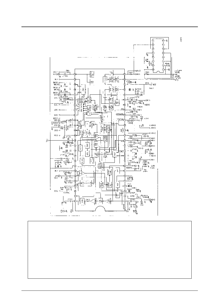
Test Circuit
LC4528