Overview
The LA7775M is an FM receiver for CATV or FM
communications equipment. In addition to functions for
FM demodulation (oscillator, mixer, limiting IF amplifier,
and quadrature detection circuits) it also includes on chip
an FSK data shaper circuit, an RF amplifier, and a local
oscillator frequency switching circuit.
Functions
∑ RF amplifier
∑ Mixer
∑ Oscillator
∑ Oscillator switching
∑ Limiting IF amplifier
∑ Quadrature detection
∑ Data shaper
Features
∑ Wideband RF input
∑ On-chip RF amplifier
∑ On-chip oscillator frequency switching circuit
Package Dimensions
unit: mm
3045B-MFP24
Monolithic Linear Integrated Circuit
Ordering number : EN5736
63097HA(OT) No. 5736-1/5
SANYO: MFP24
[LA7775M]
SANYO Electric Co.,Ltd. Semiconductor Bussiness Headquarters
TOKYO OFFICE Tokyo Bldg., 1-10, 1 Chome, Ueno, Taito-ku, TOKYO, 110 JAPAN
Wideband FSK Receiver
LA7775M
Parameter
Symbol
Conditions
Ratings
Unit
Maximum supply voltage
V
CC
max
7
V
Allowable power dissipation
Pd max
350
mW
Operating temperature
Topr
≠20 to +75
∞C
Storage temperature
Tstg
≠55 to +125
∞C
Specifications
Maximum Ratings
at Ta = 25∞C
Parameter
Symbol
Conditions
Ratings
Unit
Recommended supply voltage
V
CC
5
V
Operating supply voltage range
V
CC
op
4.5 to 5.5
V
Input frequency
fin21, fin24
40 to 350
MHz
Operating Conditions
at Ta = 25∞C
No. 5736-2/5
LA7775M
Parameter
Symbol
Conditions
Ratings
Unit
min
typ
max
Current drain
I
CCO
20
26
mA
Preamplifier input capacitance
Ci21
100 MHz
7
pF
Preamplifier input resistance
Ri21
100 MHz
1
k
Preamplifier voltage gain
Gp
350 MHz
15
dB
Mixer input capacitance
Ci24
100 MHz
7
pF
Mixer input resistance
Ri24
100 MHz
1
k
Mixer conversion gain
Gc
350 MHz
25
dB
≠3 dB limiting sensitivity
Vi
F = 75 kHz dev, at 1 kHz
10
16
dBµ
Demodulation output
Vo
F = 75 kHz dev, at 1 kHz
180
250
mVrms
SAW switching threshold level
V19TH
1.35
1.50
1.65
V
Data output high level
V18H
4.5
V
Data output low level
V18L
0.5
V
Oscillator output
V2
117.2 MHz
0.35
Vp-p
Operating Characteristics
at Ta = 25∞C (V
CC
= 5 V, f
o
= 106.5 MHz, fIF = 10.7 MHz)
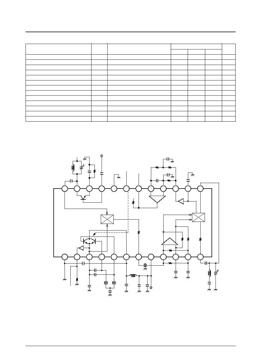
Equivalent Circuit Block Diagram and Test Circuit
PRE AMP
LIM.AMP
FM DET
OSC
RF GND
MIXER
SFE10.7MS2
117.2 MHz
119.2 MHz
390
510
1k
2 k
1 k
330
390
10 k
10 k
DATA
SHAPER
24
23
22
21
20
19
18
17
16
15
14
13
1
2
3
4
5
6
7
8
9
10
11
12
220 pF
470 pF
470 pF
0.1
µ
F
0.01
µ
F
0.01
µ
F
0.033
µ
F
43 pF
0.033
µ
F
0.01
µ
F
47
µ
F
1
µ
H
3.9
µ
H
0.01F
1000 pF
20 pF
20 pF
6 pF
20 pF
2200 pF
13 pF
2200 pF
5 pF
100 nH
GND
OSC
OUTPUT
V
CC
V
CC
V
CC
T00078
LO
SELECT DATA
OUTPUT
RF
INPUT
No. 5736-3/5
LA7775M
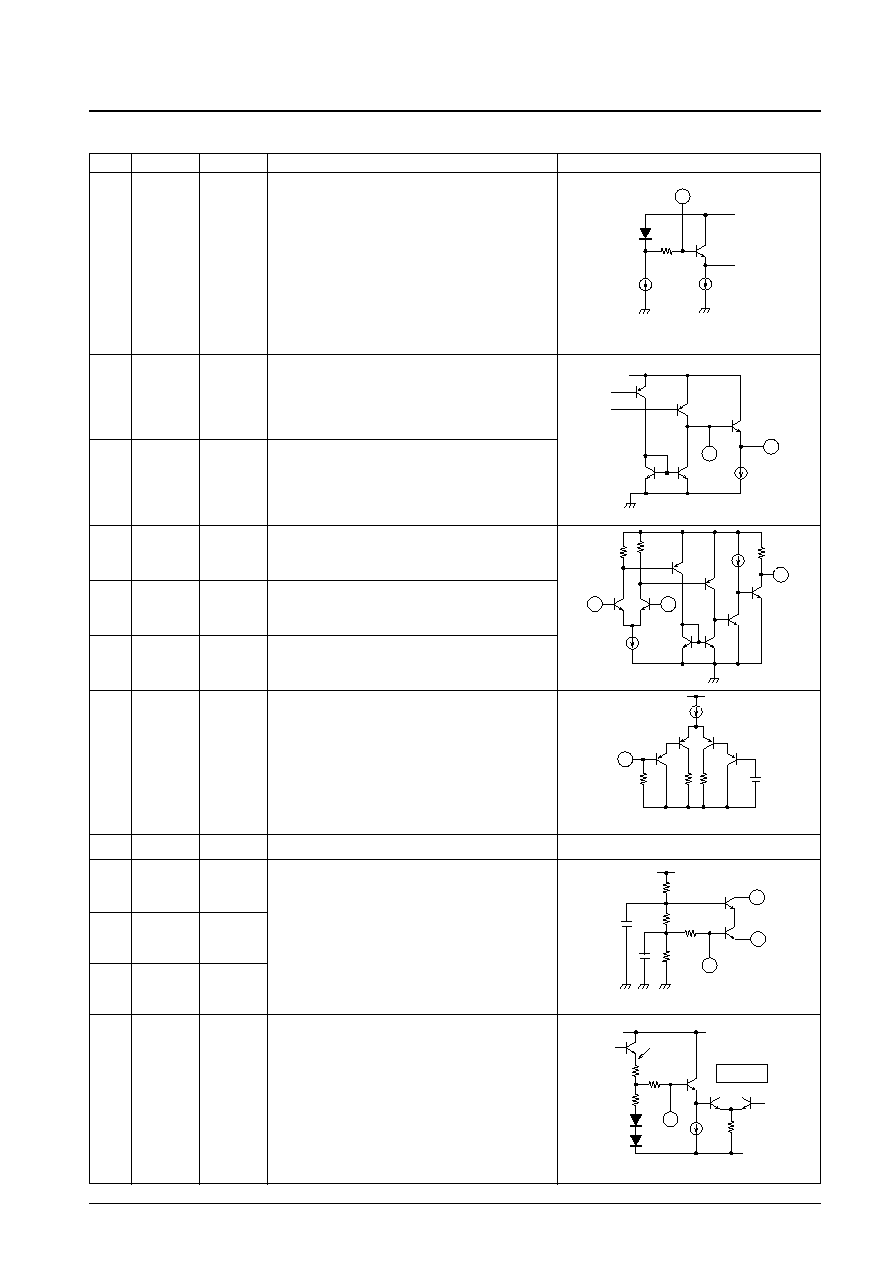
Pin Functions
Pin No.
Pin
Pin voltage(V)
Notes
Equivalent circuit
1
RFGND
2
LOOUT
3.3
Oscillator output after the limiting amplifier. This pin is used
when constructing a PLL synthesizer or related circuit. A 1-
k
external resistor is required when using this pin.
3
LOCOM
1.2
When pin 19 is low, pin 4 is selected, when high, pin 5 is
selected.
4
LORES1
1.9
5
LORES2
0.8
6
RFV
CC
7
IFOUT
4.1
A matching resistor for the SAW filter is built in.
8
V
CC
9
LIMITER
INPUT1
1.5
Insert a 510-
resistor between pins 9 and 11 when using
this circuit.
10
LIMITER
INPUT2
1.5
11
LMITER
BIAS
1.5
12
LIMITER
OUTPUT
4.2
Continued on next page.
2
3
100 mA
T00079
3
4
5
19
T00080
Switching
circuit
1 k
1 k
330
7
T00081
8 pF
4 pF
0.5 mA
50k
50k
1k
330
9
11
10
T00082
390
V
CC
12
T00083
LIMITER AMP
No. 5736-5/5
LA7775M
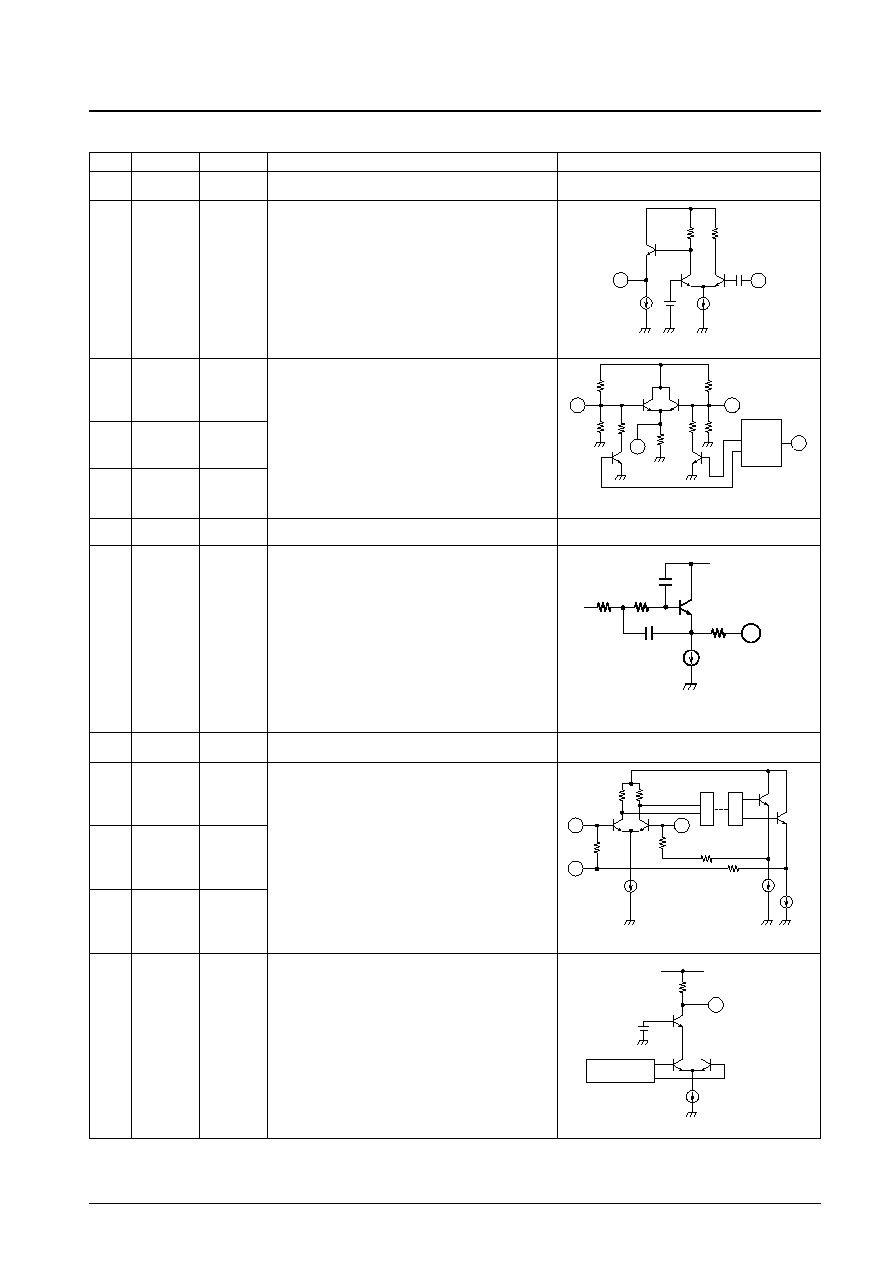
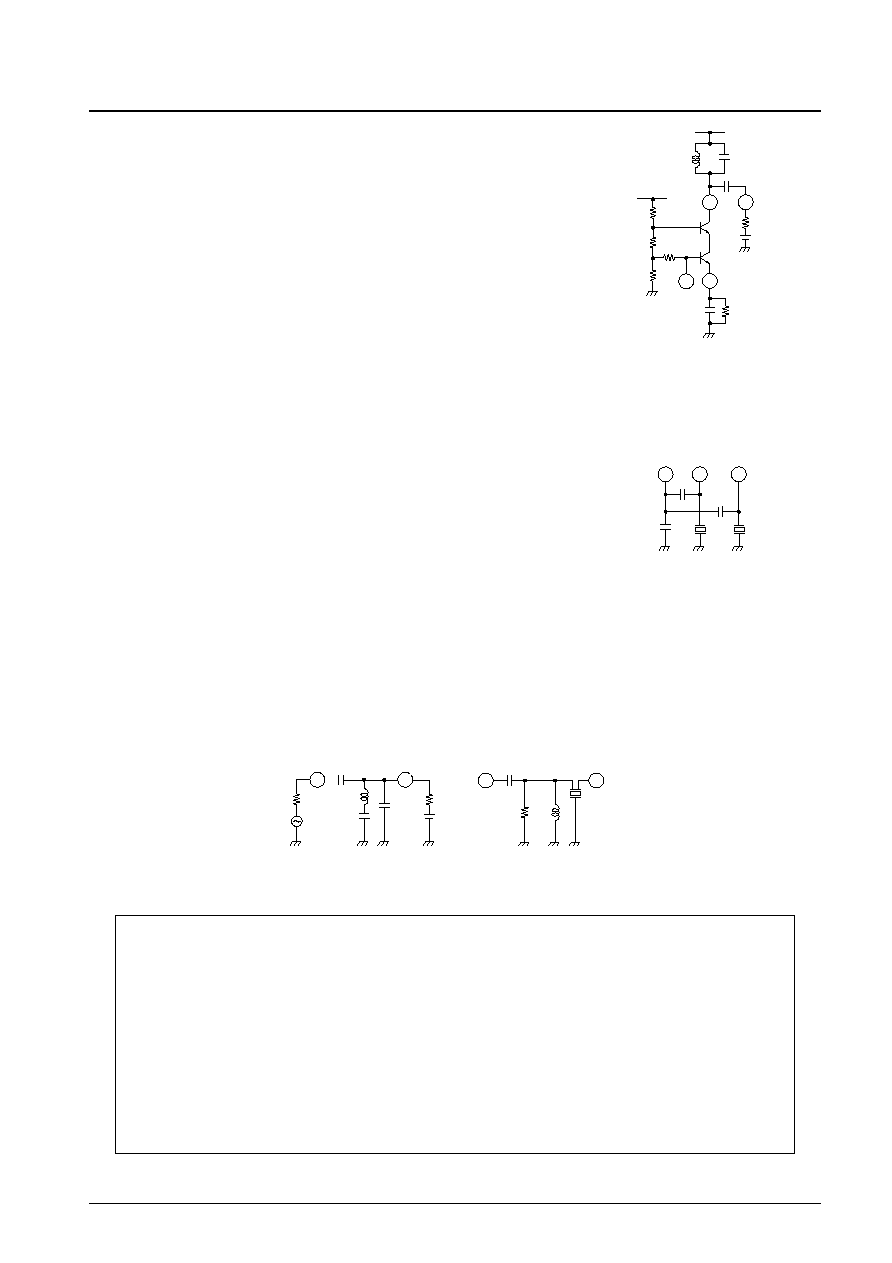
Design Notes
1. RF amplifier
This circuit is formed as a two-transistor cascode amplifier and takes an LC tank
circuit as its load. The operating current is set by the external resistor connected to
pin 22. The optimal operating current is between 1.5 and 2 mA. The capacitor
(C2) connected between pins 23 and 24 is related to the tank circuit Q, and must
not be too large.
2. Oscillator circuit
This is a grounded collector oscillator circuit, and supports using either an LC, a crystal, or a SAW resonator. Care is
required when constructing this circuit, since the input sensitivity may be suppressed if the oscillator circuit output
leaks into the IF limiting amplifier. It is extremely important to use a capacitor (e.g. a ceramic capacitor) with
excellent high-frequency characteristics for the 1000 pF bypass capacitor inserted between the oscillator circuit power
supply pin (pin 6) and the ground pin (pin 1). In addition, this capacitor must be located as close as possible to pins 1
and 6. When forming an oscillator circuit using a SAW resonator, the optimal values for C1 through C3 will vary
with the oscillator frequency. Thus this circuit must be adjusted for optimal
performance. Since the capacitor C3 between pin 3 and ground will be shared if a
circuit that switches between two SAW resonators is used, the difference between
the frequencies must be held to under 10 MHz. If a large frequency difference is
required, design a circuit that also switches the capacitance between pin 3 and
ground.
3. IF limiting amplifier
This circuit consists of a six-stage direct coupled differential amplifier to which DC feedback is applied. Since an
internal 1-k
resistor is built in between the IF input pin (pin 9) and pin 11, the input and output impedance of the
330-
IF filter can be matched with an external 510-
resistor. No external matching resistor is required for the IF
output (pin 7), since a 330-
resistor is built in.
4. Quadrature detection circuit
An external phase shifting circuit is formed from an LC tuning circuit and a ceramic discriminator.
This catalog provides information as of June, 1997. Specifications and information herein are subject to change
without notice.
s
No products described or contained herein are intended for use in surgical implants, life-support systems, aerospace
equipment, nuclear power control systems, vehicles, disaster/crime-prevention equipment and the like, the failure of
which may directly or indirectly cause injury, death or property loss.
s
Anyone purchasing any products described or contained herein for an above-mentioned use shall:
Accept full responsibility and indemnify and defend SANYO ELECTRIC CO., LTD., its affiliates, subsidiaries and
distributors and all their officers and employees, jointly and severally, against any and all claims and litigation and all
damages, cost and expenses associated with such use:
Not impose any responsibility for any fault or negligence which may be cited in any such claim or litigation on
SANYO ELECTRIC CO., LTD., its affiliates, subsidiaries and distributors or any of their officers and employees
jointly or severally.
s
Information (including circuit diagrams and circuit parameters) herein is for example only; it is not guaranteed for
volume production. SANYO believes information herein is accurate and reliable, but no guarantees are made or implied
regarding its use or any infringements of intellectual property rights or other rights of third parties.
21
22
23
C1
C2
T00090
24
3
4
5
C1
C2
C3
T00091
T00092
12
13
4 k
W
390
W
12
13
T00093