 | –≠–ª–µ–∫—Ç—Ä–æ–Ω–Ω—ã–π –∫–æ–º–ø–æ–Ω–µ–Ω—Ç: LA7780M | –°–∫–∞—á–∞—Ç—å:  PDF PDF  ZIP ZIP |
Any and all SANYO products described or contained herein do not have specifications that can handle
applications that require extremely high levels of reliability, such as life-support systems, aircraft's
control systems, or other applications whose failure can be reasonably expected to result in serious
physical and/or material damage. Consult with your SANYO representative nearest you before using
any SANYO products described or contained herein in such applications.
SANYO assumes no responsibility for equipment failures that result from using products at values that
exceed, even momentarily, rated values (such as maximum ratings, operating condition ranges, or other
parameters) listed in products specifications of any and all SANYO products described or contained
herein.
Overview
The LA7780M is a downconverter for QPSK data
demodulation for digital CATV transmission. This IC
integrates a preamplifier, an AGC amplifier, a mixer, an
oscillator, a post-amplifier, and other circuits in a single
chip, and provides all the functions required from cable
signal input through output to the A/D converter.
Features
∑ Since a preamplifier is built in, the LA7780M has
adequate sensitivity to handle the input signal from the
cable directly.
(Input signal level:≠30 to +30 dBm)
∑ Both internal and external AGC are supported as the
AGC amplifier drive technique.
∑ The output amplitude of the post amplifier used to drive
the A/D converter is 2 Vp-p (typical).
∑ Applications can be designed to use either a crystal or an
inductor oscillator.
Functions
∑ Preamplifier
∑ AGC amplifier
∑ Mixer
∑ Oscillator
∑ Post amplifier
∑ IF AGC (internal/external)
∑ AGC detector
Package Dimensions
unit: mm
3108-MFP24D
0.25
24
13
15.3
1
1
2
0.67
0.4
1.27
7.9
9.2
10.5
0.625
2.55max
2.25
0.1
Monolithic Linear IC
D1698RM (OT) No. 5268-1/9
SANYO: MFP24D
[LA7780M]
SANYO Electric Co.,Ltd. Semiconductor Bussiness Headquarters
TOKYO OFFICE Tokyo Bldg., 1-10, 1 Chome, Ueno, Taito-ku, TOKYO, 110-8534 JAPAN
QPSK Downconverter for CATV Systems
LA7780M
Ordering number : EN5268A
Parameter
Symbol
Conditions
Ratings
Unit
Maximum supply voltage
V
CC
max
Pins 5, 6, and 17
7.0
V
Circuit voltage
V max
Pins 4, 12, and 24
V
CC
V
I
4
The pin 4 output current
30
mA
Circuit current
I
13
The pin 13 sink current
2
mA
I
16
The pin 16 sink current
2
mA
Allowable power dissipation
Pd max
Ta
70∞C
540
mW
Operating temperature
Topr
≠20 to +70
∞C
Storage temperature
Tstg
≠55 to +150
∞C
Specifications
Maximum Ratings
at Ta = 25∞C

No. 5268-2/9
LA7780M
Parameter
Symbol
Conditions
Ratings
Unit
min
typ
max
Circuit current
I
total
Pins 4, 5, 6, and 17: no signal
64
80
95
mA
RF input frequency range
f
(in)
Pins 1, 8, and 9
30
150
MHz
IF output level
V
O(IF)
Pin 13:
*
1
1.6
2.0
2.5
Vp-p
IF output IM3
V
O(IM3)
Pin 13:
*
2
40
dB
IF output frequency bandwidth
BW
Pin 13:
*
3
15
MHz
Local oscillator frequency range
f
(LO)
Pins 18, 19, 20, and 21
30
200
MHz
AGC amplifier input sensitivity
Vin(RF2)
Pins 8 and 9:
*
4
≠25
≠21
≠17
dBmV
AGC range
GR
Pin 13: IF output level < ±1 dB
60
80
dB
AGC flatness
V
O(IF)
Pin 13: Compare with the state when
≠1
0
+1
dB
Vin (RF2) = 30 dBmV
Preamplifier gain
G
(RF1)
Pin 4:
*
5
17
19
21
dB
Maximum preamplifier output level
V
Omax
Pin 4:
*
6
50
dBmV
Oscillator output level
V
O(OSC)
Pin 23: The pin 23 frequency is 1/2 that of
500
800
1000
mVp-p
the local oscillator
AC Characteristics
at Ta = 25∞C, V
CC
= 5.0 V, internal AGC mode, Pin 24 is left open.
Operating Modes
Mode
Pin 10
Pin 11
Pin 12
Internal AGC
GND
With a capacitor between
Connected to pin 11
pin 11 and ground
External AGC
GND
With a capacitor between
External AGC voltage supply
(Narrow control range: 3 to 5 V)
(AGC divider inactive)
pin 11 and ground
Pin 12 = high impedance
External AGC
Open
With a capacitor between
External AGC voltage supply
(Wide control range: 0 to 5 V)
(AGC divider active)
pin 11 and ground
Pin 12 = low impedance (14 k
)
Internal AGC
External AGC
Caution:
Note 1.
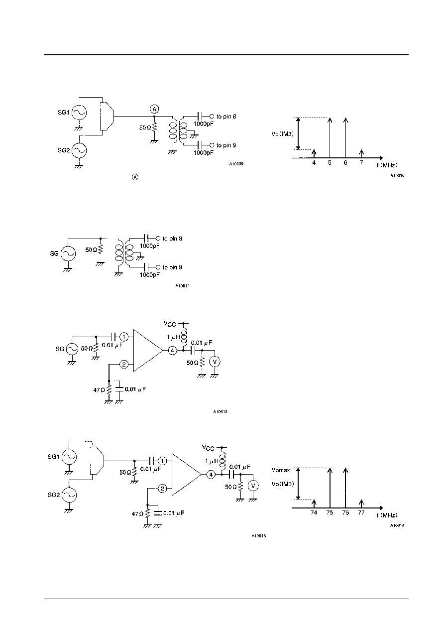
Input: SG = 69.55 MHz, 20 dBm V
Other conditions:
Internal AGC mode
Pin 24 left open.
Output: The post amplifier output (pin 13) at 5 MHz
Note: In internal AGC mode, the IF output level can be adjusted by varying the pin 24 DC voltage.
Parameter
Symbol
Conditions
Ratings
Unit
Recommended supply voltage
V
CC
Pins 5, 6, and 17
5.0
V
Operating supply voltage range
V
CC
op
Pins 5, 6, and 17
4.5 to 5.5
V
Operating Conditions
at Ta = 25∞C
Transfer ratio = 1 : 1
No. 5268-3/9
LA7780M
Note 2.
Input: SG1 = 69.55 MHz, SG2 = 70.55 MHz
Other conditions:
Internal AGC mode
Pin 24 left open.
Output: The post amplifier output (pin 13)
Note 3.
Post amplifier output level = ≠3 dB
Remove the low-pass filter between pins 14 and 16.
(Short the coil of 27 µH and remove the capacitors of 27 pF and 15 pF.)
Note 4.
Input: SG1 = 69.55 MHz
Note 5.
SG = 75 MHz, 20 dBm V
Note 6.
SG1 = 75 MHz, SG2 = 76 MHz,
Adjust the pin 1 level until the IM3 in the pin 4 output is 40 dB.
Output:RF1-OUT (pin 4)
V
O(IM3)
= 40 dB
Other conditions:
Internal AGC mode
Pin 24 left open.
Output: The signal level such that the post
amplifier output (pin 13) falls by ≠3 dB.
Point
= 20 dBmV (69.55 MHz) + 20 dBmV (70.55 MHz)
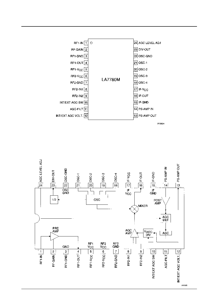
Pin Assignment
No. 5268-4/9
LA7780M
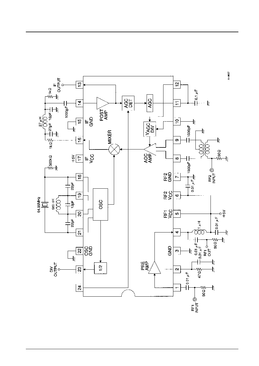
Block Diagram
Usage Notes
∑ The oscillator may stop if the power supply rise time is extremely short. To prevent this problem, insert a 500 k
resistor between pin 18 and ground or between pin 21 and ground. (This applies when a crystal oscillator is used.)
∑ This IC should be used with the pin 13 output level between 1 Vp-p and 2 Vp-p.
∑ Use a low-pass filter with a 6-dB attenuation between pins 14 and 16.
∑ Since the high-frequency process is adopted, care must be taken to prevent the influence of static electricity.
Top view
No. 5268-5/9
LA7780M
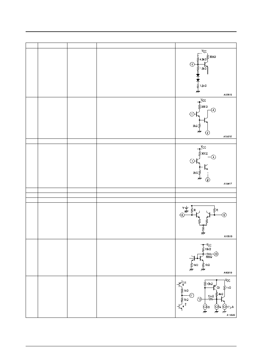
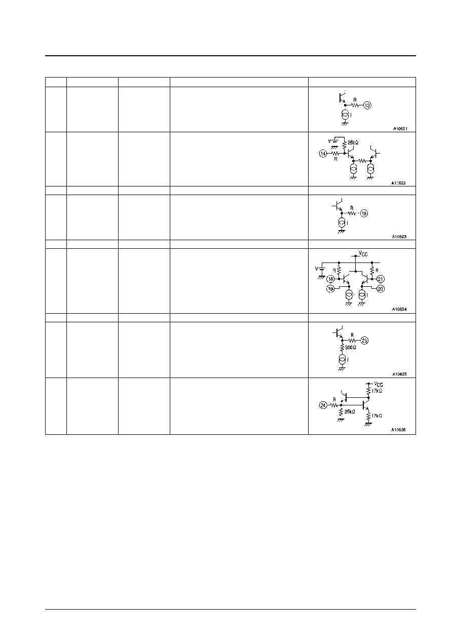
Pin No.
Function
Pin voltage (V)
Note
Equivalent circuit
1
RF1 input
2.8
Impedance connected to pin 2 must be > 45
2
RF gain
1.3
3
GND
0
4
RF1 output
Open collector
5
V
CC
5.0
6
V
CC
5.0
7
GND
0
V = 2.5 V
R = 1 k
8
9
RF2 input (1)
RF2 input (2)
2.5
2.5
Pin 10
GND : Internal or external AGC
(narrow control range)
Pin 10
open : External AGC (wide control range)
10
Internal/external
AGC switch
0 (GND)
1.0 (open)
I1 = 20 µA
I2 = 100 µA
I3, I4 & Q1 are switched on and off by pin 10.
11
12
AGC filter 2
AGC filter 1
Open collector
Open base
(Pin 10
GND)
4.0 (Pin 10 open)
Continued on next page.
Pin Descriptions
No. 5268-6/9
LA7780M
Continued from preceding page.
Pin No.
Function
Pin voltage (V)
Note
Equivalent circuit
13
Post-amp output
2, 3
R = 30
I = 7 mA
14
Post-amp input
2.0
V = 2.1 V
R = 300
15
GND
0
16
IF output
1.7
R = 100
I = 3.5 mA
17
V
CC
5.0
18
19
20
21
Oscillator input 4
Oscillator input 3
Oscillator input 2
Oscillator input 1
3.0
3.0
V = 3.0 V
R = 5 k
I = 1 mA
22
GND
0
23
Divider output
3.3
R = 100
I = 1 mA
24
Output level
adjustment
2.5
R = 25 k
Test Circuit
No. 5268-7/9
LA7780M
No. 5268-8/9
LA7780M
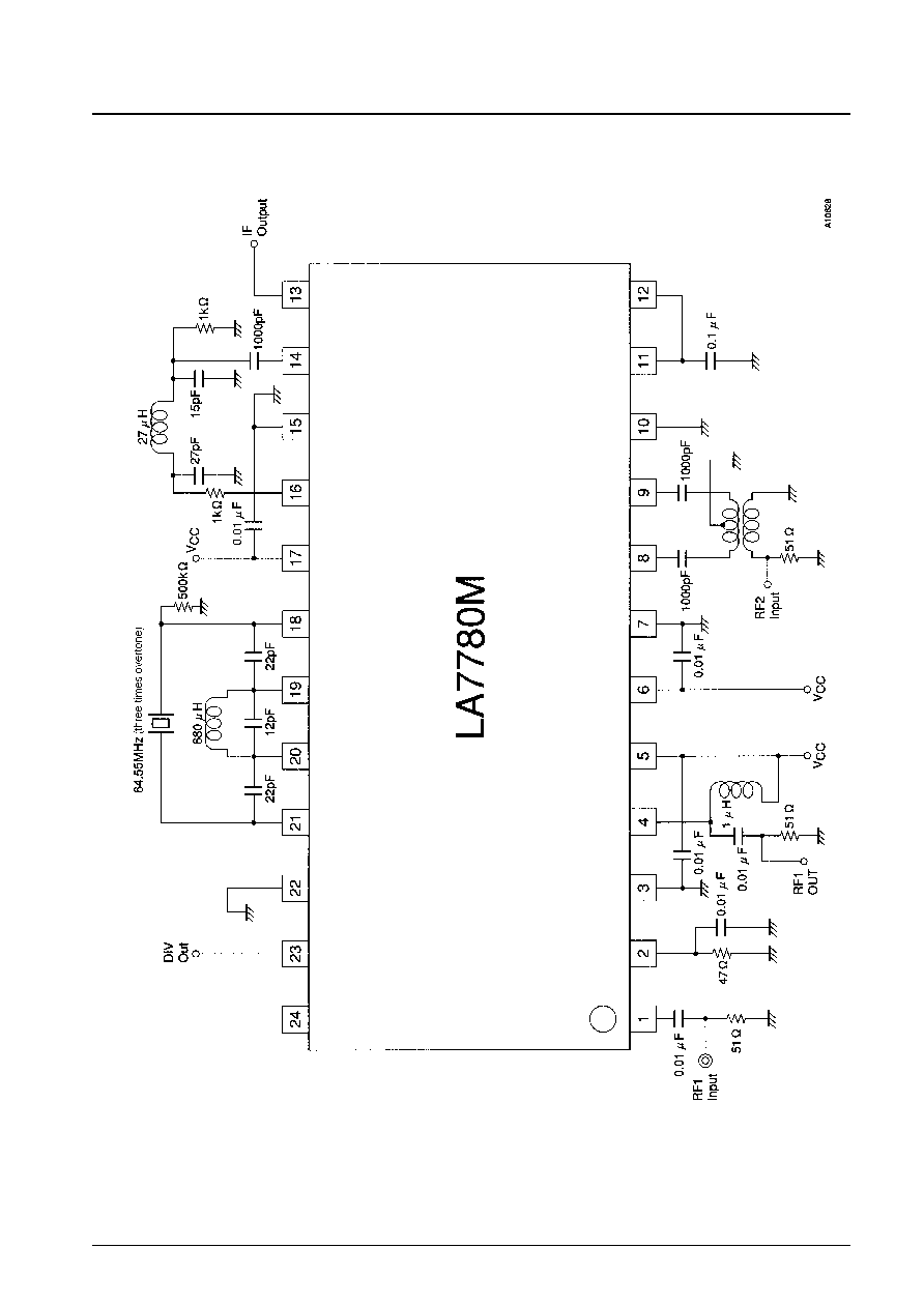
Sample Application Circuit
*
:
The choke coil between pins 19 and
20 is not required if the fundamental
frequency of the crystal (not an
overtone) is used.

PS No. 5268-9/9
LA7780M
This catalog provides information as of October, 1998. Specifications and information herein are subject
to change without notice.
Specifications of any and all SANYO products described or contained herein stipulate the performance,
characteristics, and functions of the described products in the independent state, and are not guarantees
of the performance, characteristics, and functions of the described products as mounted in the customer's
products or equipment. To verify symptoms and states that cannot be evaluated in an independent device,
the customer should always evaluate and test devices mounted in the customer's products or equipment.
SANYO Electric Co., Ltd. strives to supply high-quality high-reliability products. However, any and all
semiconductor products fail with some probability. It is possible that these probabilistic failures could
give rise to accidents or events that could endanger human lives, that could give rise to smoke or fire,
or that could cause damage to other property. When designing equipment, adopt safety measures so
that these kinds of accidents or events cannot occur. Such measures include but are not limited to protective
circuits and error prevention circuits for safe design, redundant design, and structural design.
In the event that any or all SANYO products (including technical data, services) described or contained
herein are controlled under any of applicable local export control laws and regulations, such products must
not be exported without obtaining the export license from the authorities concerned in accordance with the
above law.
No part of this publication may be reproduced or transmitted in any form or by any means, electronic or
mechanical, including photocopying and recording, or any information storage or retrieval system,
or otherwise, without the prior written permission of SANYO Electric Co., Ltd.
Any and all information described or contained herein are subject to change without notice due to
product/technology improvement, etc. When designing equipment, refer to the "Delivery Specification"
for the SANYO product that you intend to use.
Information (including circuit diagrams and circuit parameters) herein is for example only; it is not
guaranteed for volume production. SANYO believes information herein is accurate and reliable, but
no guarantees are made or implied regarding its use or any infringements of intellectual property rights
or other rights of third parties.