 | –≠–ª–µ–∫—Ç—Ä–æ–Ω–Ω—ã–π –∫–æ–º–ø–æ–Ω–µ–Ω—Ç: LA7790M | –°–∫–∞—á–∞—Ç—å:  PDF PDF  ZIP ZIP |
Overview
The LA7790M is a QPSK data transmitter for digital cable
TV applications. By integrating the I/Q quadrature
modulator, RF amplifier, electronic volume control, mute
control, and other functions onto a single chip, parts count
is reduced and set size is miniaturized.
Features
∑ Maximum RF amplifier output level of +10 dBm (75
terminator), suitable for directly driving the cable.
∑ RF output frequency range of 5 to 70 MHz. Frequency
range selection function permits broadband designs.
∑ Electronic volume control for direct-current control of
RF output level.
∑ Muting ensures ample attenuation during periods with
no transmission.
∑ Support for both internal and external bias for I/Q
modulation inputs.
∑ Support for I/Q modulation frequencies up to 10 MHz.
(typ: 500 mVp-p)
Functions
∑ I/Q quadrature modulator
∑ I/Q input bias power supply
∑ RF amplifier
∑ Varactor diode-based VCO
∑ Muting
∑ Electronic volume control
∑ Power-saving modes
∑ Switchable output frequency range
∑ Power supply voltage of 5 V (4.5 to 5.5 V)
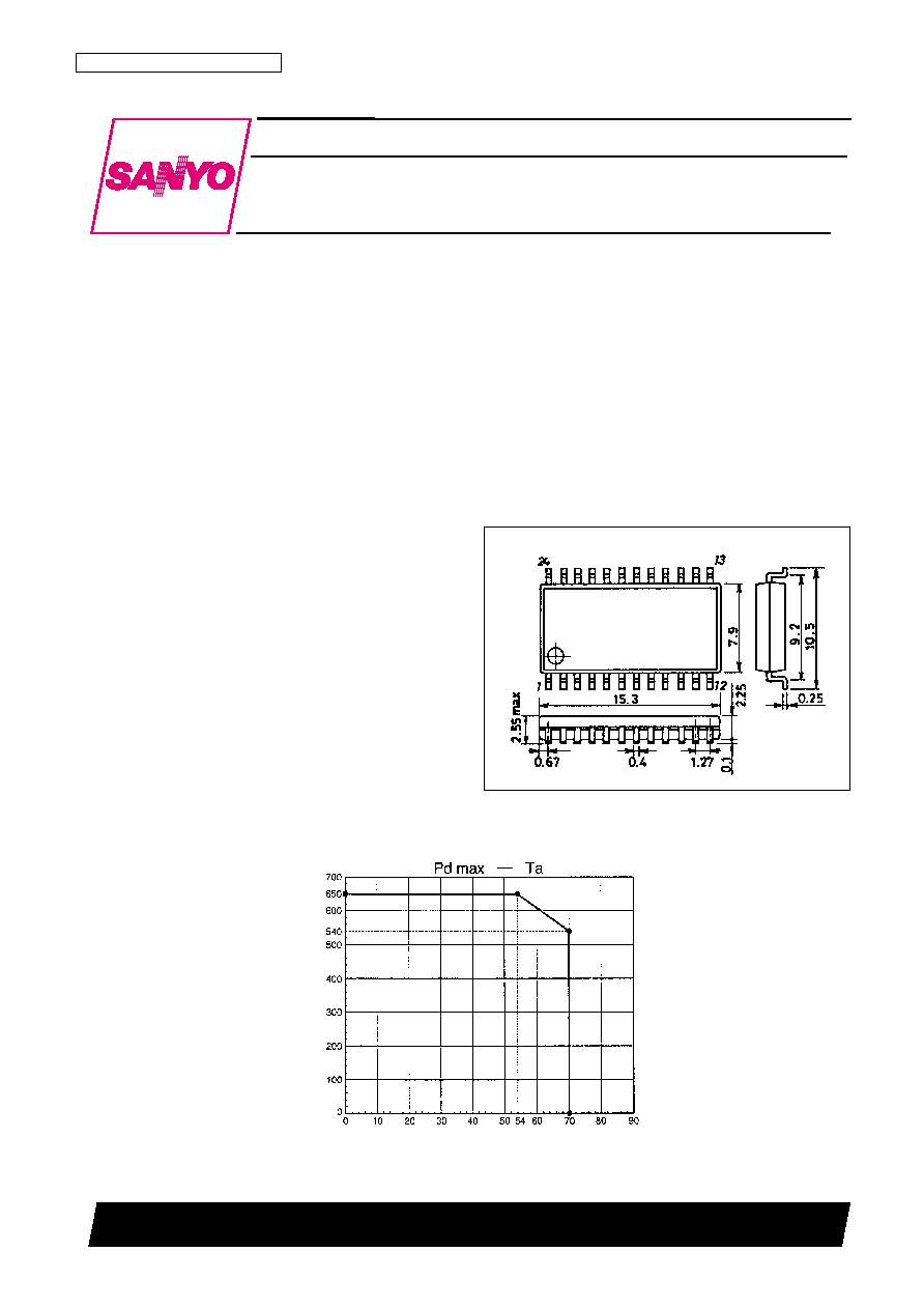
Package Dimensions
unit: mm
3108-MFP24D
Monolithic Linear IC
5061998RM (OT) No. 5689-1/14
SANYO: MFP24D
[LA7790M]
SANYO Electric Co.,Ltd. Semiconductor Bussiness Headquarters
TOKYO OFFICE Tokyo Bldg., 1-10, 1 Chome, Ueno, Taito-ku, TOKYO, 110 JAPAN
QPSK Transmitter for Cable TV
LA7790M
Ordering number : EN5689A
Ambient temperature, Ta (∞C)
Allowable power dissipation, Pd
max
(mW)
No. 5689-2/14
LA7790M
Parameter
Symbol
Conditions
Ratings
Unit
Maximum power supply voltage
V
CC
max
Pins 1, 10, and 24
7
V
Circuit voltage
Vmax
Pins 1, 12, 17, 20, 21, and 23
V
CC
V
Circuit current
I
11
Output lead-in current
1
mA
I
19
2
mA
Allowable power dissipation
Pd max
Ta
54∞C
650
mW
Operating ambient temperature
Topr
≠20 to +70
∞C
Storage temperature
Tstg
≠55 to +150
∞C
Specifications
Maximum Ratings
at Ta = 25∞C
Parameter
Symbol
Conditions
Ratings
Unit
min
typ
max
Current drain
Circuit current 1
I
1
With no signal, pin 1
26
33
44
mA
Circuit current 2
I
24
+ I
10
With no signal, pins 24 and 10
44
55
73
mA
Modulator fo: f(V19) = 25 MHz
Output frequency range
f
(V19)
5
70
MHz
Output signal level
V
19(DSB)
Note 1: V
20
= V
23
= GND,
≠7
≠4
≠2
dBm
V
12
= V
17
= V
21
= V
CC
, S1 = A
Output harmonic distortion
V
19(HD2)
Note 2: V
20
= V
23
= GND,
40
dB
V
19(HD3)
V
12
= V
17
= V
21
= V
CC
, S1 = A
35
dB
Output secondary harmonic distortion
V
19(2fo)
Note 3: V
20
= V
23
= GND,
20
dB
V
12
= V
17
= V
21
= V
CC
, S1 = A
Output tertiary harmonic distortion
V
19(3fo)
Note 3: V
20
= V
23
= GND,
8
dB
V
12
= V
17
= V
21
= V
CC
, S1 = A
Carrier suppression ratio
V
19(fo)
Note 4: V
20
= V
23
= GND,
30
dB
V
12
= V
17
= V
21
= V
CC
, S1 = A
Sideband suppression ratio
V
19(SSB)
Note 5: V
20
= V
23
= GND,
30
dB
V
12
= V
17
= V
21
= V
CC
, S1 = A
I input level
V
4.5
V
4.5
= |V
4
-- V
5
|
500
mVp-p
Q input level
V
8.9
V
8.9
= |V
8
-- V
9
|
500
mVp-p
I input DC voltage
V
4, 5
External DC bias voltage
1.9
2.1
2.3
V
Q input DC voltage
V
8, 9
External DC bias voltage
1.9
2.1
2.3
V
Reference voltage
V
6
Internal DC bias voltage
1.9
2.1
2.3
V
Variable attenuator
Minimum gain control voltage
V
21
V
12
= V
17
= V
CC
, V
20
= V
23
= GND, S1 = A
0
0.5
V
Gain range
V
19(GR)
Note 6: V
20
= V
23
= GND, V
12
= V
17
= V
CC
,
45
dB
S1 = A, V
21
= V
CC
0.5 V
Modulator output impedance
R
19
V
12
= V
17
= V
21
= V
CC
,
80
120
160
V
20
= V
23
= GND, S1 = A
VCO
Oscillator frequency range
f
(osc)
V
12
= V
17
= V
21
= V
CC
,
20
280
MHz
V
20
= V
23
= GND, S1 = A
VCO output level
V
11(fo)
V
12
= V
17
= V
21
= V
CC
,
500
700
900
mVp-p
V
20
= V
23
= GND, S1 = A
VCO output impedance
R
11
V
12
= V
17
= V
21
= V
CC
,
200
300
400
V
20
= V
23
= GND, S1 = A
Band switch
Band switch 1 "H" level
V
17H
Note 7: V
12
= V
21
= V
CC
,
4
V
f(V19) = 25 MHz
V
20
= V
23
= GND, S1 = A
Band switch 1 "L" level
V
17L
Note 7: V
12
= V
21
= V
CC
,
1
V
f(V19) = 12.5 MHz
V
20
= V
23
= GND, S1 = A
Operating Characteristics
at Ta = 25∞C, V
CC
= 5.0 V
Parameter
Symbol
Conditions
Ratings
Unit
Operating power supply voltage
V
CC
op
Pins 1, 10, and 24
4.5 to 5.5
V
Recommended Conditions
at Ta = 25∞C
Continued on next page.
No. 5689-3/14
LA7790M
Parameter
Symbol
Conditions
Ratings
Unit
min
typ
max
Band switch 2 "H" level
V
12H
Note 7: V
17
= V
21
= V
CC
,
4
V
f(V
11
) = 25 MHz
V
20
= V
23
= GND, S1 = A
Band switch 2 "L" level
V
12L
Note 7: V
17
= V
21
= V
CC
,
1
V
f(V
11
) = 12.5 MHz
V
20
= V
23
= GND, S1 = A
RF output amplifier
Maximum output level
V
1
max
Note 8: V
12
= V
17
= V
21
= V
CC
,
7
10
13
dBm
V
20
= V
23
= GND, SG3 = ≠6 dBm, S1 = A
V
1(HD2)
Note 8: V
12
= V
17
= V
21
= V
CC
,
40
dBc
Maximum output distortion
V
20
= V
23
= GND, SG3 = ≠6 dBm, S1 = A
V
1(HD3)
40
dBc
Muting
Muting on voltage
V
23H
V
12
= V
17
= V
21
= V
CC
,
4
V
V
20
= GND, S1 = B
Muting off voltage
V
23L
V
12
= V
17
= V
21
= V
CC
,
1
V
V
20
= GND, S1 = B
Muting attenuation
V
1(mute)
Note 9: V
23
= 1 V
4 V
70
dB
V
12
= V
17
= V
21
= V
CC
, V
20
= GND, S1 = B
Power save function
Power save on voltage
V
20H
4
V
Power save off voltage
V
20L
1
V
Power save current
I
1
Note 10: V
20
= 4 V
0
0.1
mA
Continued from preceding page.
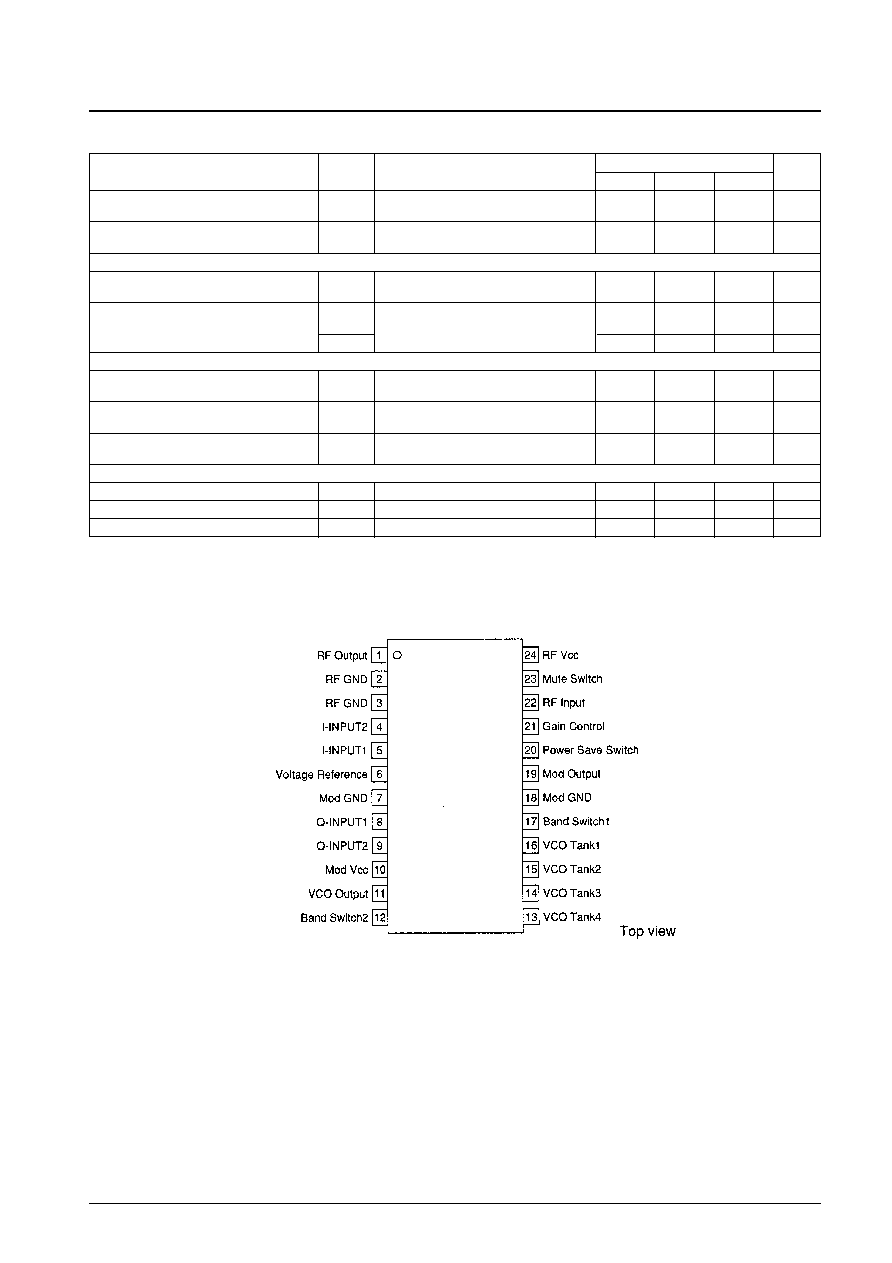
Pin Assignment
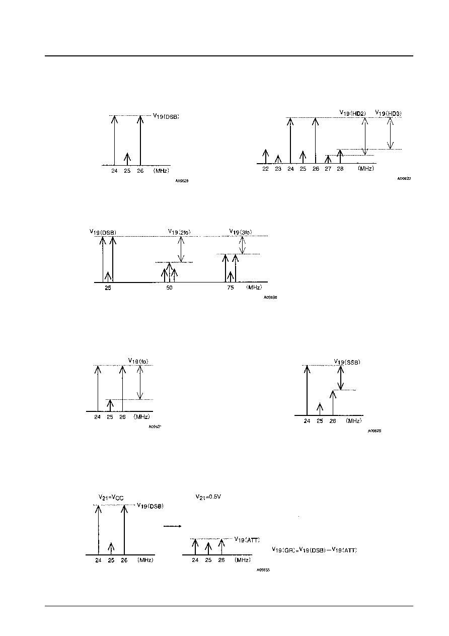
Note 1
Input: SG1 =1 MHz CW, 500 mVp-p, SG2 = No Signal or
SG2 = 1 MHz CW, 500 mVp-p, SG1 = No Signal
Output:
Note 2
Input: Same as Note 1
Output:
No. 5689-4/14
LA7790M
Note 4
Input: SG1 = SG2 = 1 MHz CW, 500 mVp-p
Output:
Note 6
Input: SG1 = 1 MHz CW, 500 mVp-p
Output:
Note 5
Input: SG1 = 1 MHz CW, 500 mVp-p, 0deg
SG1 = 1 MHz CW, 500 mVp-p, 90deg
Output:
Note 3
Input: Same as Note 1
Output:
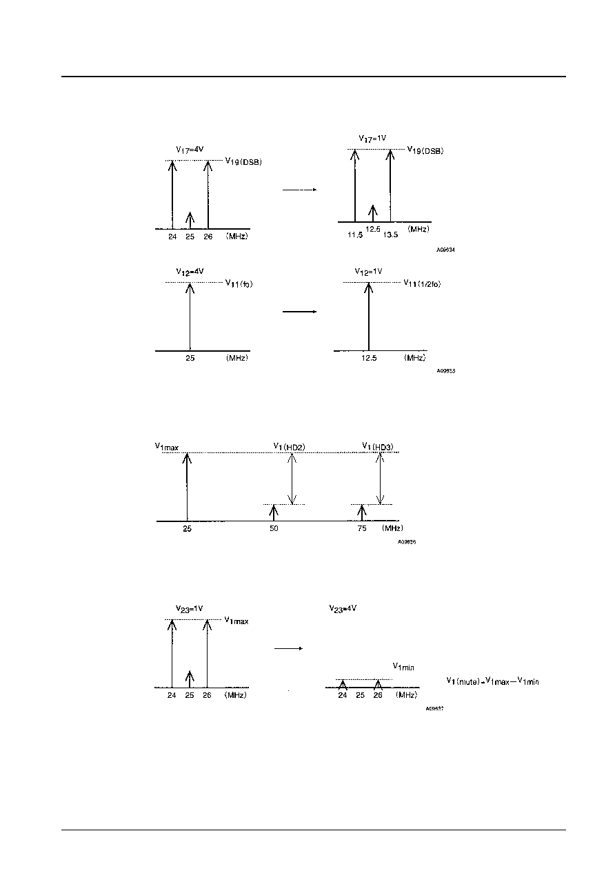
No. 5689-5/14
LA7790M
Note 7
Input: SG1 = 1 MHz CW, 500 mVp-p
Output:
Note 8
Input: SG3 = 25 MHz CW, ≠6 dBm
Output:
Note 9
Input: SG1 = 1 MHz CW, 500 mVp-p
Output:
Note 10
I
1
= pin 1 current when V20 = 4 V (power save on).