 | –≠–ª–µ–∫—Ç—Ä–æ–Ω–Ω—ã–π –∫–æ–º–ø–æ–Ω–µ–Ω—Ç: LA7975 | –°–∫–∞—á–∞—Ç—å:  PDF PDF  ZIP ZIP |

PAL SIF Converter Circuit
for TV and VCR Multi-system
Overview
The LA7975 is an IC that converts PAL SIF signals (5.5 MHz,
6 MHz, and 6.5 MHz) to 6 MHz. For the sake of high sound
quality, this IC uses a unique mixer technique to supress
interference from NICAM signals.
Functions
.
Mixer, amplifier, oscillator, oscillator mute
Features
.
Resistant to interference by NICAM signals
.
Small SIP-5 package
.
Wide range of usage voltage (5 V to 12 V)
Package Dimensions
unit : mm
3042C-SIP5
[LA7975]
SANYO : SIP5
Specifications
Maximum Ratings
at Ta = 25∞C
Parameter
Symbol
Conditions
Ratings
Unit
Maximum supply voltage
V
CC
max
13.2
V
Maximum feed current
I
5
max
3
mA
I
4
max
1
mA
Allowable power dissipation
Pd max
Ta
%
70∞C
200
mW
Operating temperature
Topr
≠20 to +70
∞C
Storage temperature
Tstg
≠40 to +150
∞C
Operating Conditions
at Ta = 25∞C
Parameter
Symbol
Conditions
Ratings
Unit
Recommended supply voltage
V
CC
9
V
Operating voltage range
V
CC
op
5 to 12
V
Ordering number: EN3994B
Monolithic Linear IC
LA7975
SANYO Electric Co.,Ltd. Semiconductor Bussiness Headquarters
TOKYO OFFICE Tokyo Bldg., 1-10, 1 Chome, Ueno, Taito-ku, TOKYO, 110 JAPAN
73096HA(II)/8282TS No.3994-1/6
Operating Characteristics
at Ta = 25∞C, V
CC
= 9 V
Parameter
Symbol
Conditions
Test point
min
typ
max
Unit
Current drain
I
CC
Pin 2
5
6.5
9
mA
Conversion gain
5.5 MHz
G5.5
80 dB/µV input
Pin 5
10
13.5
17
dB
6.5 MHz
G6.5
80 dB/µV input
Pin 5
10
13.5
17
dB
6.0 MHz
G6.0
80 dB/µV input, Pin 4
grounded with 10 k
Pin 5
18.5
22
25.5
dB
Oscillation level
V
OSC
Pin 4
15
36
80
mVp-p
Maximum output level
V
O
max
5.5 MHz 100 dB/µV input
Pin 5
109
112
115
dB/µV
Input impedance
Ri
5.5 MHz input
4.8
k
Pin voltages
V1
Pin 1
2.6
3
3.4
V
V4
Pin 4
7.6
8
8.4
V
V5
Pin 5
7.2
7.6
8
V
500 kHz level difference
relative to 6 MHz
OSC leak
Pin 5
30
44
dB
Maximum input level
V
IN
max
90
dB/µV
Oscillation stop current
I
4
Pin 4
300
µA
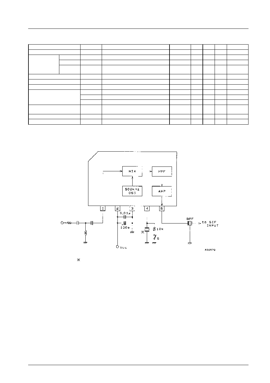
Sample Application Circuit
Unit (resistance:
, capacitance: F)
Oscillator
500 kHz CSB503E5
Murata Industries, Ltd.
1.5 MHz CSA1.500MK2
Murata Industries, Ltd.
500 kHz EFOA500K04S
Matsushita Electric, Ltd.
LA7975
No.3994-2/6
Reference Example 1
Reference Example 2
Unit (resistance:
, capacitance: F)
LA7975
No.3994-3/6
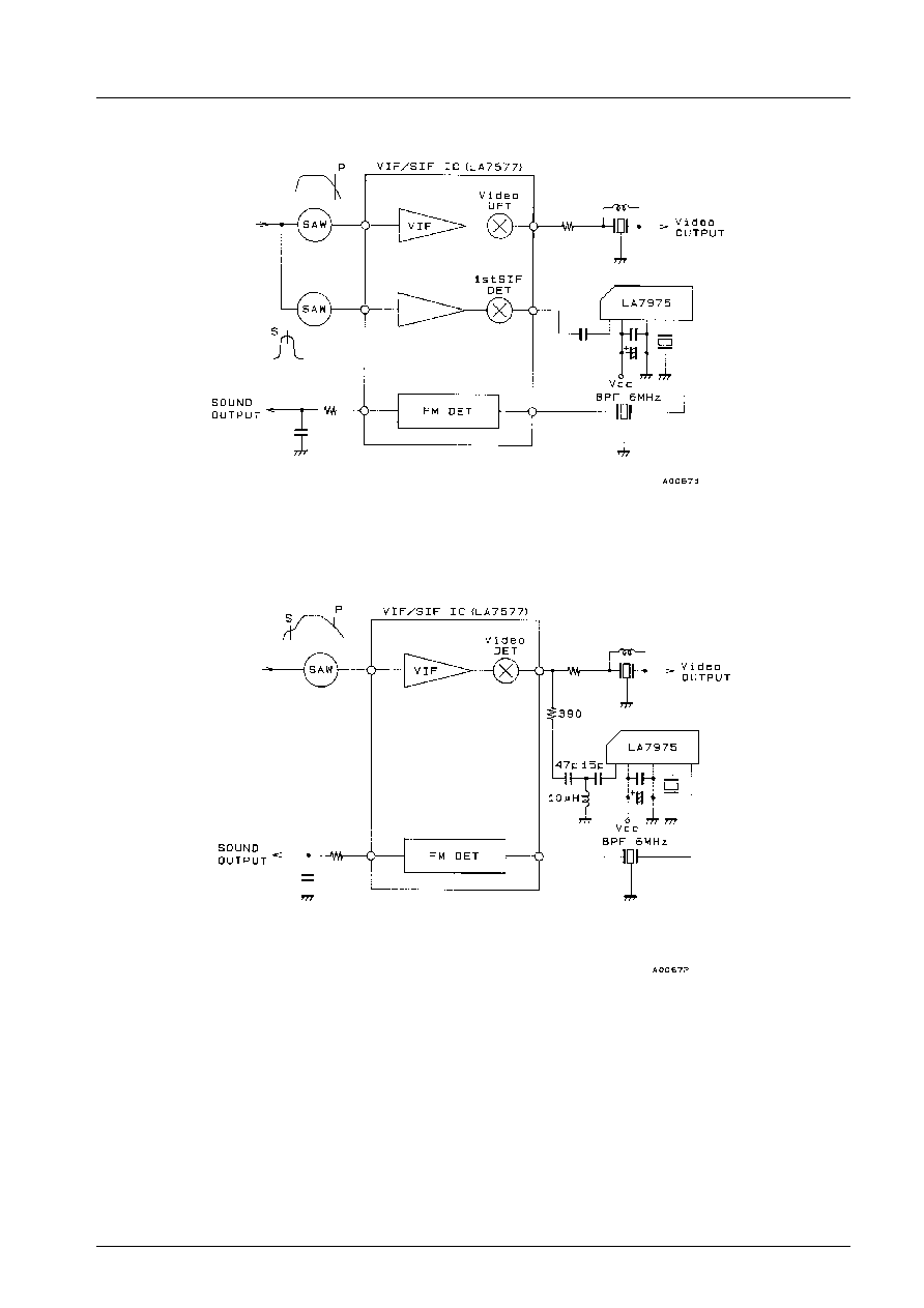
.
Pin 1 is the SIF input pin.
The filter in Figure 2 can be connected to the input section
to improve the buzz characteristic.
Figure 3 shows the characteristics for the filter in Figure 2.
If C1 is too small, the buzz characteristic improves for
normal input, but the filter cuts into the sound carrier and the
buzz characteristic deteriorates for the P/S (picture/sound
carrier) ratio.
Use C1
6 20 pF to 47 pF.
.
Pin 4 is the ceramic oscillator pin.
To make the oscillation waveform approach a sine wave,the
oscillation level is controlled internally.
Oscillation levels of 15 to 80 mVp-p at Pin 4 give the
waveform shown in Figure 5.
To stop oscillation, attach an external resistor as in Figure 6
and switch S1 on.
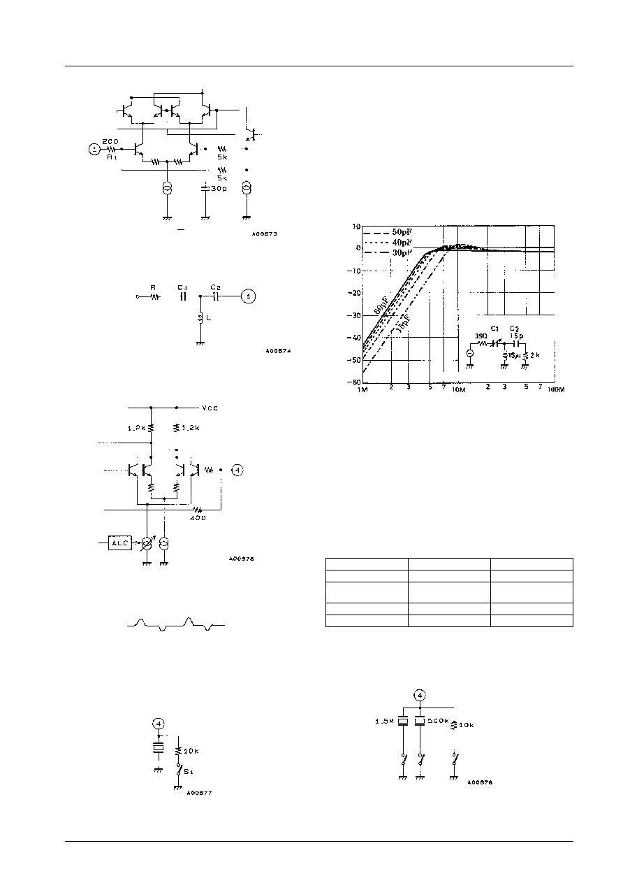
Here are the conditions for handling multiple systems.
Input frequency
Oscillator
Pin 5 output
5.5 MHz
500 kHz
6 MHz
6.0 MHz
Oscillation stop
6 MHz
(pass through)
6.5 MHz
500 kHz
6 MHz
4.5 MHz
1.5 MHz
6 MHz
Figure 7
Figure 8 shows a proposed multi-system
Unit (resistance:
, capacitance: F)
Figure 1
From video
output section
Figure 2
Unit (resistance:
)
Figure 4
Figure 5
(Pin 4 oscillation waveform)
Figure 6
Unit (resistance:
)
Filter characteristic
Attenuation
≠
d
B
Unit (resistance:
, capacitance: F)
Frequency ≠ Hz
Figure 3
(Multi-system implementation)
Figure 8
Unit (resistance:
)
LA7975
No.3994-4/6
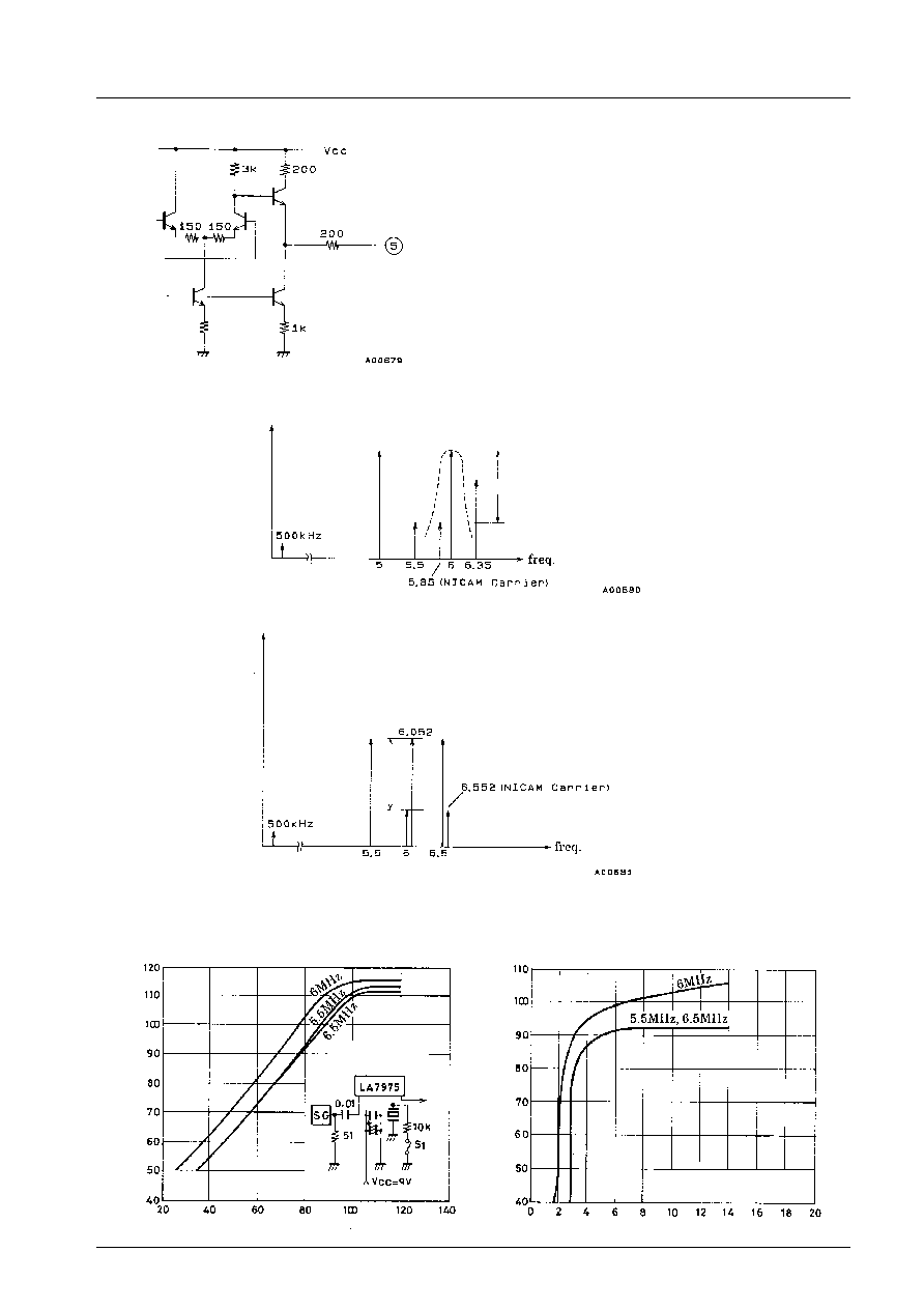
.
Pin 5 is the output pin. The output from Pin 5 is input to the
SIF via a 6 MHz bandpass filter (BPF).
When 5.5 MHz is input to Pin 1, the spectrum shown in
Figure 10 is obtained at Pin 5. Even if there is a 5.85 MHz
NICAM signal, the D/U (desirable/undesirable) ratio at Pin 5
increases and the buzz characteristic does not deteriorate.
When 6 MHz is input at Pin 1 and there is a 6.552 MHz
NICAM signal, then 6.552 MHz is mixed with 500 kHz to
make 6.052 MHz. This becomes an interference signal and is
within the band for 6 MHz. Therefore,for 6 MHz input, Pin 4
is grounded with 10 k
to stop the oscillation and pass
through the input signal 6 MHz as is.
Reference Characteristic Diagram
Unit (resistance:
)
Figure 9
Output level
Ceramic BPF
chracteristic
D/U ratio
Figure 10 (5.5 MHz input)
Output level
Interference obtained with LA7975 mixer
6.552 MHz ≠ 500 kHz = 6.052 MHz
D/U
ratio
Figure 11 (6 MHz input)
Input/output characteristic
Output
level,
V
O
≠
dB/µV
Input level ≠ dB/µV
* S1 on for 6 MHz
measurement
Unit (resistance:
, capacitance: F)
Output
level,
V
O
≠
dB/µV
V
O
≠ V
CC
* Input level 80 dB/µV S1 on
for 6 MHz measurement
Supply voltage, V
CC
≠ V
LA7975
No.3994-5/6

No products described or contained herein are intended for use in surgical implants, life-support systems, aerospace equipment,
nuclear power control systems, vehicles, disaster/crime-prevention equipment and the like, the failure of which may directly or
indirectly cause injury, death or property loss.
Anyone purchasing any products described or contained herein for an above-mentioned use shall:
1
Accept full responsibility and indemnify and defend SANYO ELECTRIC CO., LTD., its affiliates, subsidiaries and distributors
and all their officers and employees, jointly and severally, against any and all claims and litigation and all damages, cost and
expenses associated with such use:
2
Not impose any responsibility for any fault or negligence which may be cited in any such claim or litigation on SANYO
ELECTRIC CO., LTD., its affiliates, subsidiaries and distributors or any of their officers and employees jointly or severally.
Information (including circuit diagrams and circuit parameters) herein is for example only; it is not guaranteed for volume
production. SANYO believes information herein is accurate and reliable, but no guarantees are made or implied regarding its use
or any infringements of intellectual property rights or other rights of third parties.
This catalog provides information as of July, 1996. Specifications and information herein are subject to change without notice.
f ≠ V
CC
Oscillation
frequency
,f≠k
H
z
Oscillation stop voltage 3.7 V
Supply voltage, V
CC
≠ V
Oscillation
level
≠
mVp-p
Oscillation level ≠ V
CC
Supply voltage, V
CC
≠ V
Oscillation level ≠ R
Oscollation
level
≠
mVp-p
FET probe
Series resistance, R ≠
LA7975
No.3994-6/6