
71598RM(KI) No. 5920-1/5
LA7995M
Charge Pump Type DC-DC Converter
Monolithic Linear IC
Overview
This DC-DC converter IC supplies 30V from a V
CC
of
5V. Possible applications include use as a power
supply for tuner circuitry on a PC video board.
Conventional DC-DC converters utilize the
counterelectromotive force in a coil to step up the
voltage. This method suffers from high-frequency
noise caused by sharp pulses. The so-called charge
pump principle adopted in the LA7995M chip results in
much lower noise and also has the advantage of using
only capacitors, reducing the cost for peripheral
components.
Specifications
Maximum Ratings
at Ta = 25
�
C
Package Dimensions
unit:mm
3111-MFP14S
1
14
7
8
8.0
0.15
1.0 1.0
0.35
1.8max
1.5
0.1
4.4
6.4
5.15
0.625
SANYO Electric Co., Ltd. Semiconductor Bussiness Headquarters
TOKYO OFFICE Tokyo Bldg., 1-10, 1 Chome, Ueno, Taito-ku, TOKYO, 110-8534 JAPAN
[LA7955M]
SANYO:MFP14S
Ratings
Unit
Symbol
Parameter
Maximum supply voltage
Allowable power dissipation
Operating temperature
Storage temperature
7
380
�10 to +65
�55 to +150
V
mW
�
C
�
C
V
CC
max
Pd max Ta
65
�
C
*
Topr
Tstg
Conditions
Note: *Includes substrate (phenol) 144.3
x
76.1 x 1.6 mm
Any and all SANYO products described or contained herein do not have specifications that can handle
applications that require extremely high levels of reliability
such as life-support systems
aircraft
'
s
control systems
or other applications whose failure can be reasonably expected to result in serious
physical and/or material damage. Consult with your SANYO representative nearest you before using
any SANYO products described or contained herein in such applications.
SANYO assumes no responsibility for equipment failures that result from using products at values that
exceed
even momentarily
rated values (such as maximum ratings
operating condition ranges
or other
parameters) listed in products specifications of any and all SANYO products described or contained
herein.
Ordering number : EN5920A
71598RM(KI) No. 5920-2/5
Ratings
Unit
Symbol
Parameter
Recommended supply voltage
Operating supply voltage range
5
4.75 to 5.25
V
V
V
CC
V
CC
op
Conditions
Current drain
Output voltage
Output voltage fluctuation
Output current
Oscillation frequency
I
IN
V
OUT
V
OUT
I
OUT
f
I
O
=1 mA, V
CC
=5V
I
O
=1 mA, V
CC
=5V
I
O
=1 mA, V
IN
=4.75 to 5.25V
V
O
=29V
C
OSC
=150pF
19
29
1.5
35
24
30.7
1.0
1.7
50
29
32
1.5
65
mA
V
V
mA
KHz
Parameter
Symbol
Conditions
Ratings
min
typ
max
Unit
Operating Conditions
at Ta = 25
�
C
Operating Characteristics
at Ta = 25
�
C
Note: The above specifications are measured with external capacitance provided by three 0.33
�
F chip capacitors(C1,
C2, C3).
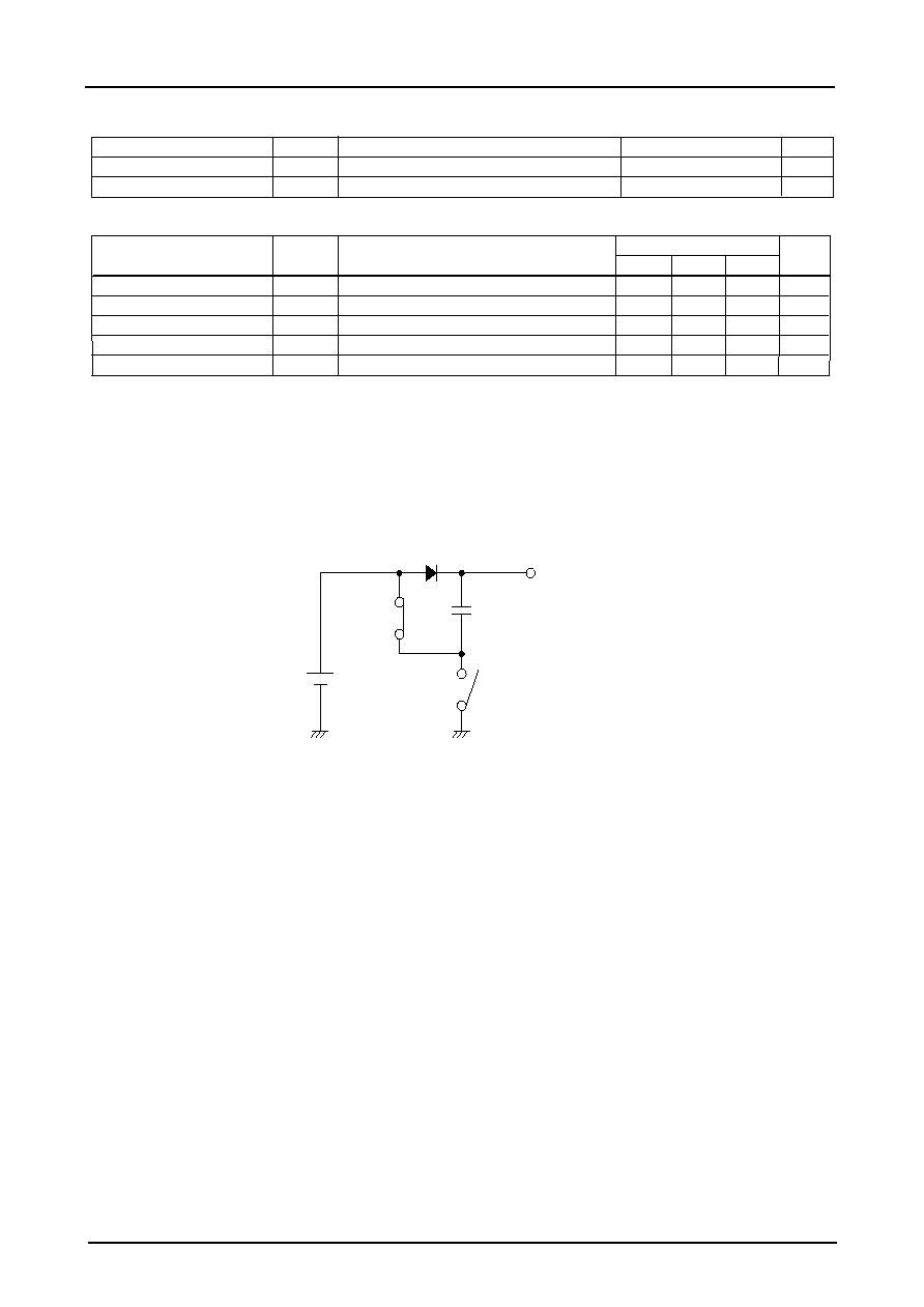
Charge Pump Principle
Figure 1 shows a charge pump circuit. Driving S1 and S2 with opposite phase produces a doubled voltage
A11009
VCC
S1
S2
VOUT2VCC
Figrue 1 Chrage pump circuit
In order to supply 30V from 5V, the LA7995M uses three charge pump circuits in series to produce a step-up factor of 2
x 2 x 2 = 8.
LA7995M
71598RM(KI) No. 5920-3/5
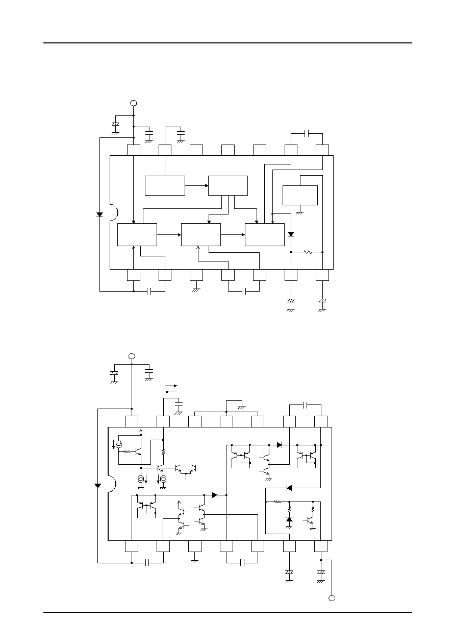
Block Diagram
The LA7995M incorporates the following functions for controlling the 3-stage charge pump circuit:
� Oscillator
� Switching circuit
Figure 2 Block diagram
1
2
3
4
5
6
7
8
9
10
11
12
13
14
0.33F
0.33F
0.33F
4.7F
4.7F
150pF
47F
0.01F
VCC=5V
Vout=30V
NC
NC
NC
A11011
Discharge200A
Charge6A
6A
100A
200A
1k
1k
VCC
200
7.5k
1k
Equivalent Internal Circuit and Recommended Peripheral Circuitry
1
2
3
4
5
6
7
8
9
10
11
12
13
14
C1
D1
C2
C3
Creg
Cout
Cosc
Cvcc1
Cvcc2
VCC=5V
NC
NC
NC
Charge pump
1
Charge pump
2
Charge pump
3
Oscillator
Switching
circuit
30V zener
diode circuit
A11010
LA7995M

71598RM(KI) No. 5920-4/5
Test Circuit
1
2
3
4
5
6
7
8
9
10
11
12
13
14
0.33F
D1
0.33F
0.33F
4.7F
4.7F
150pF
10nF
47F
V-14
R-1
NC
NC
NC
Charge pump
1
Charge pump
2
Charge pump
3
Oscillator
Switching
circuit
30V zener
diode circuit
A11012
V-7
Current consumption
Output voltage
Output voltage fluctuation
Output current I
OUT
I
IN
V
OUT
V
OUT
Connect a DC current generator to V-7 and use an
ammeter to measure the current supplied to V-14 when
1mA is drawn from V-7.
Mesure voltage at V-7.
Vary power supply voltage from 4.75 to 5.25V. Measure
voltage change at V-7.
Measure output current required to obtain 29V from V-7.
Measure frequency of pulse wave form at R-1.
Item
Symbol
Test method
V-7
V-14
V-7
V-7
V-7
Measurement
point
Oscillation frequency f R-1
Output current (mA)
-
1.0
1.0
1.0
1.0
Test Method
LA7995M
71598RM(KI) No. 5920-5/5
This catalog provides information as of July, 1998. Specifications and information herein are subject to change
without notice.
PS
Specifications of any and all SANYO products described or contained herein stipulate the performance
characteristics
and functions of the described products in the independent state
and are not guarantees
of the performance
characteristics
and functions of the described products as mounted in the customer's
products or equipment. To verify symptoms and states that cannot be evaluated in an independent device
the customer should always evaluate and test devices mounted in the customer's products or equipment.
SANYO Electric Co.
Ltd. strives to supply high-quality high-reliability products. However
any and all
semiconductor products fail with some probability. It is possible that these probabilistic failures could
give rise to accidents or events that could endanger human lives
that could give rise to smoke or fire
or that could cause damage to other property. When designing equipment
adopt safety measures so
that these kinds of accidents or events cannot occur. Such measures include but are not limited to protective
circuits and error prevention circuits for safe design
redundant design
and structural design.
In the event that any and all SANYO products described or contained herein fall under strategic
products (including services) controlled under the Foreign Exchange and Foreign Trade Control Law of
Japan
such products must not be exported without obtaining export license from the Ministry of
International Trade and Industry in accordance with the above law.
No part of this publication may be reproduced or transmitted in any form or by any means
electronic or
mechanical
including photocopying and recording
or any information storage or retrieval system
or otherwise
without the prior written permission of SANYO Electric Co.
Ltd.
Any and all information described or contained herein are subject to change without notice due to
product/technology improvement
etc. When designing equipment
refer to the
"
Delivery Specification
"
for the SANYO product that you intend to use.
Information (including circuit diagrams and circuit parameters) herein is for example only
it is not
guaranteed for volume production. SANYO believes information herein is accurate and reliable
but
no guarantees are made or implied regarding its use or any infringements of intellectual property rights
or other rights of third parties.
LA7995M