
Signal Processor for Cordless Telephone Base Sets
Functions
Speech network block
c 2-wire/4-wire conversion
c Line driver
c Transmitting amplifier
c Receiving amplifier (with ATT)
c Power supply switching circuit
c Impedance matching
c DTMF interface
c Key tone interface
c BN circuit network switching circuit
(BN = Balancing Network)
Signal processor block
c Record preamplifier (with ALC)
c Record amplifier
c Power amplifier (V
CC
= 5 V, R
L
= 8
, P
O
= 200 mW)
c Playback equalizer amplifier
c Voice detector (VOX)
c Electronic volume control (4 dB, 7 steps)
Crosspoint switch block
c Crosspoint switches (mixing available)
c CPU interface
Features
c Because it is possible to switch the Balancing Network
between two systems, one for the near end and one for the
far end, in accordance with the line current, this IC provides
excellent sidetone characteristics over a wide range of line
currents.
c Receiver amplifier supports ceramic receivers and dynamic
receivers.
c Power amplifier on chip
(V
CC
= 5 V, R
L
= 8
, P
O
= 200 mW).
c Crosspoint switches allow full mixing, permitting the
implementation of a variety of functions, such as three- or
four-way calls.
c Digital volume control on chip (power system output).
Package Dimensions
unit : mm
3159-QFP64E
[LA8515NM]
SANYO : QIP64E
Allowable
power
dissipation,
Pd
max
-
W
Ambient temperature, Ta - �C
120
�
120
�
1.5 mm
3
glass epoxy board
Independent IC
Ordering number: EN5421
Monolithic Linear IC
LA8518NM
SANYO Electric Co.,Ltd. Semiconductor Bussiness Headquarters
TOKYO OFFICE Tokyo Bldg., 1-10, 1 Chome, Ueno, Taito-ku, TOKYO, 110 JAPAN
41596HA (II) No.5421-1/31

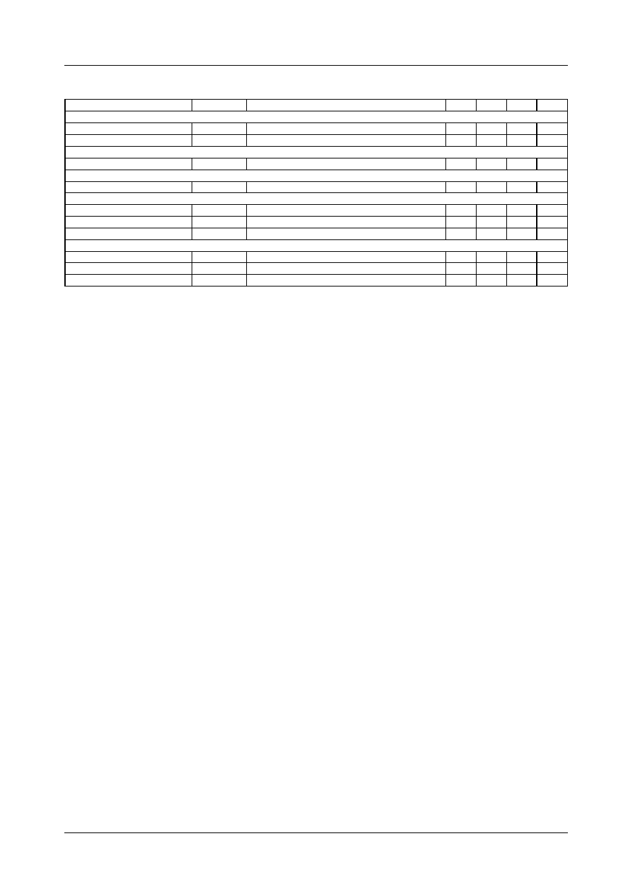
Specifications
Maximum Ratings
at Ta = 25�C
Parameter
Symbol
Conditions
Ratings
Unit
Maximum supply voltage
V
L
max
Speech network block
15
V
V
CC
max
Other than speech network block
10
V
Line current
I
L
max
130
mA
Allowable power dissipation
Pd max
1.05
W
Operating temperature
Topr
�20 to +70
�C
Storage temperature
Tstg
�40 to +150
�C
Operating Conditions
at Ta = 25�C
Parameter
Symbol
Conditions
Ratings
Unit
Recommended supply voltage
V
CC
Other than speech network block
5
V
Operating supply voltage range
V
CC
op
4.5 to 7.5
V
Operating Characteristics
at Ta = 25�C, f = 1 kHz
Parameter
Symbol
Conditions
min
typ
max
Unit
[Speech Network Block (External power supply operating characteristics)]
Line voltage
V
L
I
L
= 20 mA
3.3
3.9
4.3
V
I
L
= 50 mA
4.9
5.7
6.5
V
I
L
= 120 mA
7.8
9.3
10.8
V
Internal supply voltage
V
SP
I
L
= 20 mA
4.5
4.8
5.0
V
I
L
= 50 mA
4.5
4.8
5.0
V
I
L
= 120 mA
4.5
4.8
5.0
V
Transmitting gain
G
T
I
L
= 20 mA, V
IN
= �55 dBV
43
45
47
dB
I
L
= 120 mA, V
IN
= �55 dBV
39
41
43
dB
Receiving gain
G
R
I
L
= 20 mA, V
IN
= �20 dBV
�3.0
�1.0
+1.0
dB
I
L
= 120 mA, V
IN
= �20 dBV
�9.5
�7.5
�5.5
dB
DTMF gain
G
MF
I
L
= 20 mA, V
IN
= �30 dBV
28
30
32
dB
I
L
= 120 mA, V
IN
= �30 dBV
24
26
28
dB
KT gain
G
KT
I
L
= 20 mA, V
IN
= �40 dBV
9
11
13
dB
I
L
= 120 mA, V
IN
= �40 dBV
9
11
13
dB
Transmitting dynamic range
DR
T
I
L
= 20 mA, THD = 4%
2.5
Vp-p
I
L
= 120 mA, THD = 4%
4.5
Vp-p
Receiving dynamic range
(Single R
L
= 150
)
DR
DR
I
L
= 20 mA, THD = 10%
0.5
Vp-p
I
L
= 120 mA, THD = 10%
0.5
Vp-p
Receiving dynamic range
(BTL R
L
= 3 k
)
DR
SR
I
L
= 20 mA, THD = 10%
5
Vp-p
I
L
= 120 mA, THD = 10%
5
Vp-p
MUTE high-level input voltage
V
IH
I
L
= 20 mA to 120 mA
0.6VSP
V
MUTE low-level input voltage
V
IL
I
L
= 20 mA to 120 mA
0
0.4
V
Transmitting PADC attenuation
G
T
I
L
= 30 mA, ground at 24 k
3.6
dB
Receiving PADC attenuation
G
R
I
L
= 30 mA, ground at 24 k
6.5
dB
Internal reference voltage
V
REF
I
L
= 20 mA
2.3
V
I
L
= 50 mA
2.3
V
I
L
= 120 mA
2.3
V
[Speech Network Block (Operating characteristics when power is off)]
Line voltage
V
L
I
L
= 20 mA
3.3
3.8
4.3
V
I
L
= 50 mA
4.8
5.4
6.2
V
I
L
= 120 mA
7.2
8.7
10.2
V
Internal supply voltage
V
SP
I
L
= 20 mA
1.7
1.9
2.1
V
I
L
= 50 mA
2.5
2.8
3.1
V
I
L
= 120 mA
4.55
4.85
5.15
V
Continued on next page.
LA8518NM
No.5421-2/31

Continued from preceding page.
Parameter
Symbol
Conditions
min
typ
max
Unit
Transmitting gain
G
T
I
L
= 20 mA, V
IN
= �55 dBV
42
44
46
dB
I
L
= 120 mA, V
IN
= �55 dBV
39
41
43
dB
Receiving gain
G
R
I
L
= 20 mA, V
IN
= �20 dBV
�4.5
-2.5
�0.5
dB
I
L
= 120 mA, V
IN
= �20 dBV
�9
�7
�5
dB
DTMF gain
G
MF
I
L
= 20 mA, V
IN
= �30 dBV
27
29
31
dB
I
L
= 120 mA, V
IN
= �30 dBV
24
26
28
dB
KT gain
G
KT
I
L
= 20 mA, V
IN
= �40 dBV
6.7
8.7
10.7
dB
I
L
= 120 mA, V
IN
= �40 dBV
9
11
13
dB
Transmitting dynamic range
DR
T
I
L
= 20 mA, THD = 4 %
2.5
Vp-p
I
L
= 120 mA, THD = 4 %
4.5
Vp-p
Receiving dynamic range
(Single R
L
= 150
)
DR
DR
I
L
= 20 mA, THD = 10%
0.3
Vp-p
I
L
= 120 mA, THD = 10%
0.5
Vp-p
Receiving dynamic range
(BTL R
L
= 3 k
)
DR
SR
I
L
= 20 mA, THD = 10%
2
Vp-p
I
L
= 120 mA, THD = 10%
6
Vp-p
MUTE high-level input voltage
V
IH
I
L
= 20 mA to 120 mA
0.6VSP
V
MUTE low-level input voltage
V
IL
I
L
= 20 mA to 120 mA
0
0.4
V
Transmitting PADC attenuation
G
T
I
L
= 30 mA, ground at 24 k
3.7
dB
Receiving PADC attenuation
G
R
I
L
= 30 mA, ground at 24 k
6.3
dB
Internal reference voltage
V
REF
I
L
= 20 mA
0.65
V
I
L
= 50 mA
1.0
V
I
L
= 120 mA
1.7
V
Operating Characteristics
at Ta = 25�C, f = 1 kHz
Parameter
Symbol
Conditions
min
typ
max
Unit
[Audio Signal Processing Block]
PRE AMP
Input from crosspoint switch
Voltage gain
VG
C
�45 dBV input
6
8
10
dB
Total harmonic distortion
THD
�20 dBV input
0.4
1.0
%
ALC saturation output level
V
OS
�20 dBV input
90
110
130
mVrms
ALC range
ALCW
From when ALC is on until THD is 1%
15
dB
Equivalent input noise voltage
V
NI
Input AC-shorted, 20 to 20 kHz
5.0
10
�Vrms
PB AMP
Voltage gain
VG
E
�60 dBV input
46.5
48.5
50.5
dB
Total harmonic distortion
THD
�60 dBV input
0.5
1.5
%
Equivalent input noise voltage
V
NI
Pin AC-shorted, 20 to 20 kHz
5.0
10
�Vrms
OGM AMP
Voltage gain
VG
G
�20 dBV input
7
9
11
dB
Total harmonic distortion
THD
�20 dBV input
0.1
1.0
%
REC AMP
Voltage gain
VG
R
Pin 20 Z
AC
= 8.1 k
, between pins 25 and 21
4
6
8
dB
Output bias voltage
(Voltage at pin 21)
V
B
Pin 20 Z
DC
= 15 k
,
pin 21 load = 8.2 k
0.8
1.0
1.2
V
Total harmonic distortion
THD
0.8
1.5
%
MIC AMP
Voltage gain
VG
M
�40 dBV input
27
29
31
dB
Total harmonic distortion
THD
�40 dBV input
0.1
1.0
%
Equivalent input noise voltage
V
NI
Pin 33 AC-shorted, 20 to 20 kHz
2.0
5
�Vrms
POWER AMP R
L
= 8
Voltage gain
VG
P
�30 dBV input
28
30
32
dB
Output voltage
P
O
THD = 10%
200
250
mW
Total harmonic distortion
THD
�30 dBV input
0.6
1.5
%
Input resistance
R
IN
15
k
Ripple rejection ratio
SVRR
Rg = 0, fr = 100 Hz, Vr = �20 dBV
40
dB
Output noise voltage
V
NO
Pin 42 AC-shorted, 20 to 20 kHz
0.04
0.1
�Vrms
Continued on next page.
LA8518NM
No.5421-3/31
Continued from preceding page.
Parameter
Symbol
Conditions
min
typ
max
Unit
VOX
Sensitivity 1
V
OXL
�24 dBV input
0.3
V
Sensitivity 2
V
OXH
�27 dBV input
4.8
V
Electronic volume control
Step width
E
VRW
3.8
dB
VREF
Output voltage
V
REF
2.1
2.3
2.5
V
Control
Clock frequency
F
CK
500
kHz
High-level input signal
V
H
3
V
Low-level input signal
V
L
1.5
V
Power supply switch
Pin 31 voltage 1
V
CH1
The voltage applied to pin 31 is effective
3.5
V
Pin 31 voltage 2
V
CH2
The voltage supplied from pin 64 is effective
1.2
V
Quiescent current
I
CCO
Power amplifier on
19
26
35
mA
LA8518NM
No.5421-4/31
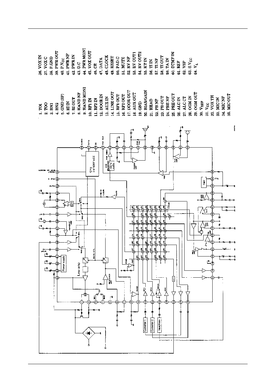
Block Diagram
LA8518NM
No.5421-5/31
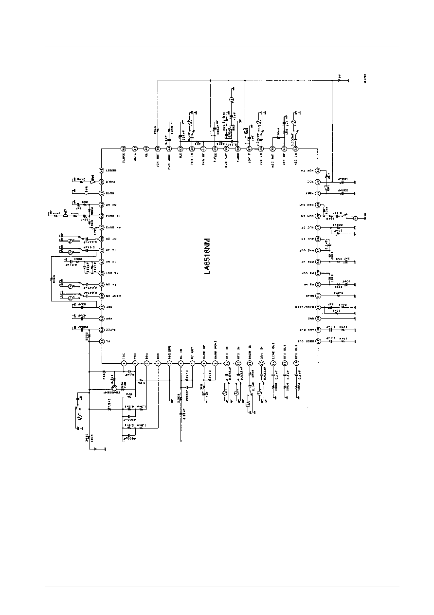
Test Circuit Diagram
LA8518NM
No.5421-6/31
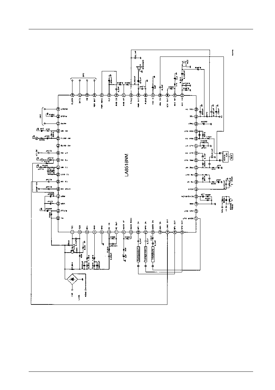
Sample Application Circuit
LA8518NM
No.5421-7/31

-- Serial control data format --
c Serial data content
A0 to A6
Specify the address of a crosspoint switch and a control switch.
D
Turns the crosspoint switch on and off and controls the control switch.
(When D = 1, the switch is on; when D = 0, the switch is off.)
c Example: Turning address 11 (AUX input, RF1 output) on
The address table is shown on the following page:
Note 1: Because there is a power-on reset function, all crosspoint switches and control switches are reset when the external power
supply (V
CC
at pin 31) is turned on.
Note 2: SW2 and SW3 in the block diagram are controlled by the MUTE pin (pin 51); the signals that are enabled are shown
below.
MUTE pin
SW2
SW3
H
Transmitting (Pin 58)
TAIN (Pin 59)
Receiving (Pin 7)
L
DTMF (Pin 60)
KT (Pin 55)
First bit
LA8518NM
No.5421-8/31

-- Address chart --
Input
LINE
HAND
RF1
RF2
DOOR
AUX
MIC
OGM
PRE
Output
LINE
--
01
02
03
--
04
05
06
--
HAND
07
--
08
09
0A
0B
--
0C
--
RF1
0D
0E
--
0F
10
11
12
13
--
RF2
14
15
16
--
17
18
19
1A
--
DOOR
--
1B
1C
1D
--
1E
1F
20
--
AUX
21
22
23
24
25
26
27
28
--
PWR
29
--
2A
2B
2C
2D
--
2E
37
PRE
2F
30
31
32
33
34
35
36
--
Other Control Switches
00
All crosspoint switches and control switches off
*2
38
Mixing switch for PB amplifier-OGM amplifier on
39
Transmitting/receiving CTL (SW1 and SW2 in the block diagram) *1
3A
Receiver amplifier ATT
Set to 0 dB
3B
Line amplifier ATT
Set to �6 dB
3C
ALC on
3D
PB amplifier on
3E
REC amplifier on
3F
Power amplifier on
40
Electronic volume control
0 dB
*2
41
Electronic volume control
�4dB
42
Electronic volume control
�8dB
43
Electronic volume control
�12dB
44
Electronic volume control
�16dB
45
Electronic volume control
�20dB
46
Electronic volume control
�24dB
47
Electronic volume control
�28dB
*1: When address 39 is on, SW1 enables the transmitting amplifier output (pin 58) signal, and SW4 enables the receiving
amplifier output (pin 7) or KT (pin 55) signal. If voltage is not supplied to pin 31 (V
CC
) (power is off), the status of SW1
and SW4 is the same as address 39 is in on state.
*2: When setting address 00 and 40 to 47, ``D'' data may be either ``0'' or ``1''.
Note 1: The receiver amplifier ATT is set to -6 dB when power is first applied, when a reset is performed, and when all of the
switches are off.
Note 2: The line amplifier ATT is set to 0 dB when power is first applied, when a reset is performed, and when all of the switches
are off.
Note 3: The electronic volume control is set to 0 dB when power is first applied, when a reset is performed, and when all of the
switches are off.
Note 4: The addresses are given in hexadecimal notation.
LA8518NM
No.5421-9/31

Input Port Timing
c f
MAX
(Maximum clock frequency)
500 kHz
c f
WL
(Clock pulse width ``L'')
1�s or longer
c f
WH
(Clock pulse width ``H'')
1�s or longer
c t
CS
(Chip enable setup time)
1�s or longer
c t
CH
(Chip enable hold time)
1�s or longer
c t
DS
(Data setup time)
1�s or longer
c t
DH
(Data hold time)
1�s or longer
c t
WC
(Chip enable pulse width)
1�s or longer
c t
WR
(Reset pulse width)
1�s or longer
Note: The control data must input 400 ms or longer after the supply voltage is applied to V
CC
(pin 31).
LA8518NM
No.5421-10/31

Pin Functions
Pin No.
Pin Name
Internal Equivalent Circuit
Pin Function
64
1
2
V
L
T
OI
T
OO
c
Line current input pin, line voltage pin.
c
Transmitting output current input pin.
c
Transmitting output current output pin.
3
4
BN1
BN2
c
BN switch pin 1.
c
BN switch pin 2. Connect when there are two
balancing network circuits. Open when not
used.
5
GND (SP)
c
Speech network system GND pin.
6
7
RI IN
RI OUT
c
Receiving input amplifier � input pin.
c
Receiving input amplifier output pin.
8
9
HAND NF
HAND MONI
c
Handset amplifier � input pin.
c
Handset amplifier output pin.
10
11
13
RF1 IN
RF2 IN
AUX IN
c
Compander 1 input pin.
c
Compander 2 input pin.
c
Unused input pin.
12
DOOR IN
c
Amplifier input pin for interphone.
Because there is a feedback resistor
(30 k
) on chip, the input is passed
through an external resistor.
Continued on next page.
LA8518NM
No.5421-11/31

Continued from preceding page.
Pin No.
Pin Name
Internal Equivalent Circuit
Pin Function
14
LINE OUT
c
Line output pin.
15
16
17
18
RF1 OUT
RE2 OUT
DOOR OUT
AUX OUT
c
Compander 1 input pin.
c
Compander 2 input pin.
c
Interphone output pin.
c
Auxiliary output pin.
19
GND
c
Signal processing system GND.
20
21
BIAS/GAIN
HEAD
c
Bias pin. The REC amplifier gain and the
REC bias gain can be controlled by an
external resistor.
c
REC amplifier output pin and PB amplifier +
input pin.
22
24
PB NF
PRE NF
c
PB amplifier - input pin.
c
PRE amplifier - input pin.
23
25
35
PB OUT
PRE OUT
MIC OUT
c
PB amplifier output pin.
c
PRE amplifier output pin.
c
MIC amplifier output pin
26
ALC IN
c
ALC input pin. Input from the PRE output (pin
25) via a coupling capacitor. In addition, the
ALC level can be adjusted by connecting
resistors in series.
Continued on next page.
LA8518NM
No.5421-12/31

Continued from preceding page.
Pin No.
Pin Name
Internal Equivalent Circuit
Pin Function
27
ALC CT
c
ALC time constant adjustment pin. Adjusts
the ALC attack time and recovery time.
28
29
OGM IN
OGM OUT
c
OGM amplifier - input pin.
c
OGM amplifier output pin.
30
VREF
c
Internal reference voltage output pin
(approx. 2.3 V).
31
V
CC
c
External power supply input pin. Supplies
power to the signal processing system and to
V
SP
(pin 62).
32
36
VOX TH
VOX IN
c
VOX sensitivity adjustment pin. The VOX
sensitivity can be adjusted by connecting this
pin to pin 30 (V
REF
) through a resistor.
c
VOX + input pin.
33
34
MIC IN
MIC NF
c
MIC amplifier + input pin.
c
MIC amplifier - input pin.
37
VOX.C
c
VOX detection pin. Can also be used as a
waveform shaper by forcing this pin high.
Continued on next page.
LA8518NM
No.5421-13/31

Continued from preceding page.
Pin No.
Pin Name
Internal Equivalent Circuit
Pin Function
38
P. GND
c
Power system GND pin.
40
P. V
CC
c
Power system power supply pin.
39
41
42
43
PWR OUT
PWR NF
PWR IN
D.C
c
Power amplifier output pin. Goes to high
impedance when MUTE is on.
c
Power amplifier - input pin.
c
Power amplifier + input pin.
c
Power amplifier reference voltage pin
(approximately 4/9
�
P. V
CC
).
44
PWR MONI
c
Output pin for power amplifier.
45
VOX OUT
c
VOX output pin. Open collector output.
46
47
48
49
CE
DATA
CLOCK
RESET
to
c
Chip enable input pin.
c
Data input pin.
c
Clock input pin.
c
Reset pin. Power-on reset.
50
PADC
c
Pad control pin. By connecting this pin to
GND or to S. V
CC
(pin 63) through a resistor,
it is possible to use the line current for gain
control and to control the operating current
for BN switching.
Continued on next page.
LA8518NM
No.5421-14/31

Continued from preceding page.
Pin No.
Pin Name
Internal Equivalent Circuit
Pin Function
51
MUTE
c
Mute pin. Switches the transmitting signal
and the DTMF signal in the transmitting
system, and the receiving signal and the KT
signal in the receiving system (SW2 and
SW3 in the block diagram). When low, the
DTMF and KT signals are valid.
52
53
54
RV NF
RV OUT1
RV OUT2
c
Receiver amplifier - input pin.
c
Receiver amplifier 1 output pin.
c
Receiver amplifier 2 output pin.
55
KT IN
c
Key tone input pin.
56
57
58
TI IN
TI NF
TI OUT
c
Transmission input amplifier + input.
Because bias voltage is not applied
internally, connect signal from REF (pin 61)
via a resistor.
c
Transmission input amplifier - input pin.
c
Transmission input amplifier output pin.
59
TA IN
c
Input pin for LINE output pin.
60
DTMF IN
c
Input for DTMF input pin.
Continued on next page.
LA8518NM
No.5421-15/31

Continued from preceding page.
Pin No.
Pin Name
Internal Equivalent Circuit
Pin Function
61
REF
Power supply
ON
(Pin 30)
c
Speech network system internal reference
voltage output. When the V
CC
(pin 31)
voltage is 3.5 V or more, V
REF
(pin 30) is
output. When the V
CC
voltage is 1.2 V or
less, voltage of approximately (2/5)
�
V
SP
is
output.
62
V
SP
c
Speech
network
system
internal
power
supply. When the V
CC
(pin 31) voltage is
3.5 V or more, (V
CC
applied voltage or
thereabout - 0.3 V) is output. When the V
CC
voltage is 1.2 V or less, (S. V
CC
(pin 63) or
thereabout - 0.3 V) is output.
63
S. V
CC
c
Speech network system power supply. When
the V
CC
(pin 31) voltage is 1.2 V or less,
voltage is supplied to V
SP
(pin 62) from the
line voltage.
LA8518NM
No.5421-16/31

Usage Explanations
c Speech network
c External Transistors
Because the IC has a built-in power amplifier, for reasons concerning allowable power dissipation, connect a transistor for
heat dissipation purposes as shown in Fig. 1 so that the line current is consumed externally from the IC. In addition, when
establishing the allowable power for R1 and R2, take into consideration the maximum line current that can be expected.
* When oscillation is generated due to the load state between V
L
-GND, insert C1 (about 0.1�F).
c DC resistance conversion method
By varying R2 in Fig. 1, it is possible to change the DC resistance. (Refer to the graphs below.)
* Note that varying R2 will also change the transmitting system gain and the balancing network conditions.
c AC impedance setting method
The AC impedance is basically determined by R3 (620
) and C2 (220 �F) in Fig. 1. Because AC loads other than the speech
network will be placed on the line, adjust the AC impedance in conjunction with the speech network impedance.
* Note that varying R3 changes the DC resistance.
Fig. 1
Line
LA8518NM
DC characteristics (Power on)
Line
voltage,
V
L
-V
Line current, I
L
- mA
Line
voltage,
V
L
-V
DC characteristics (Power off)
Line current, I
L
- mA
LA8518NM
No.5421-17/31

c Balancing Network
It is possible to switch the Balancing Network between two systems, one for the near end and one for the far end, in accordance
with the line current. (Refer to Fig. 1 for the connection method.) In addition, the switching point can be varied by connecting the
PADC pin (pin 50) to GND or to S. V
CC
(pin 63) via a resistor.
(When using only one Balancing Network, refer to Fig. 2.)
Note) The constant of Balancing Network is a reference value.
c The DC characteristics when the power is off
By connecting a load to V
SP
(pin 62), it is possible to change the DC characteristics without changing the DC characteristics only
when the power is off. (Refer to the diagram below.)
Fig. 2
Line
LA8518NM
Load
LA8518NM
DC characteristics (Power on)
Line
voltage,
V
L
-V
Line current, I
L
- mA
Line
voltage,
V
L
-V
DC characteristics (Power off)
Line current, I
L
- mA
No load
No change
LA8518NM
No.5421-18/31
c Receiver Amplifier Application Circuit
1 When using the dynamic receiver
2 When using the ceramic receiver
c The Receiver Amplifier Attenuator
Normally, the attenuator is set to -6 dB. It is set to 0 dB when serial data 3A is on.
LA8518NM
No.5421-19/31
c Gain Distribution
*1 I
L
= 20 mA
*2 I
L
= 120 mA
Note 1) Terminal of line 600
*1 I
L
= 20 mA
*2 I
L
= 120 mA
*3 When serial data 3A is turned on.
Note 2) The gain values are approximate values.
Note 3) The values shown in parentheses can be varied externally.
Line drive
amp
Transmitting
Transmitting
amp
Balancing
Network
Receiving input
amp
Receiving
Receiving
output amp
Attenuation
LA8518NM
No.5421-20/31

Speech Network Block Switch Operation
SW2 and SW3 are controlled by pin 51 (MUTE), while SW1 and SW4 are controlled by the serial data (address 39). (SW2 and
SW3, and SW1 and SW4 are coupled to each other.)
SW1, SW4 operation
Condition
SW1
SW4
Power on (Initial state)
1
1
Address 39 on
2
2
Power off
2
2
* When the power is off, SW1 and SW2 are fixed at ``2'' and
cannot be switched.
SW2, SW3 operation
Pin 51 (MUTE)
SW2
SW3
High
1
1
Low
2
2
* SW2 and SW3 operate as shown in the table at left,
regardless of whether the power is on or off.
Power supply
Line amp
LA8518NM
No.5421-21/31
c LINE amplifier attenuator
Normally, the attenuator is set to 0 dB. It is set to -6 dB when serial data 3 dB is on.
c REC amplifier V/I conversion
In order to derive the recording current for the DC bias, this circuit performs V/I conversion. The conversion gain and the bias
current can be controlled by the external resistor connected to pin 20. Current equal to the current output from pin 20 is output
from pin 22.
DC bias current = 2.3 V/(100
+ 15 k
)
6 150 �A
Signal current = 1.0 Vp-p/(100
+ 15 k
//22 k
)
6 110 �Ap-p
c VOX
1 The VOX circuit determines whether or not conversation is taking place. If the VOX input (pin 36) signal is -24dB or
higher, the VOX output (pin 45) goes low. The output level is adjusted by inserting a resistor between VOX TH (pin 32)
and V
REF
(pin 30).
2 Because the circuit can be used as a waveform shaper by connecting VOX C (pin 37) to V
CC
(setting pin 37 high), a
400 Hz beep tone can be detected.
Crosspoint switch
PB input
V
IN
= 0.3 V
P-P
PRE Amp output level
Internal reference voltage 2.3 V
(Open collector output)
LA8518NM
No.5421-22/31

c Power amplifier application
* The phase compensation capacitor C2 should be located near the IC.
* When muting (address 3F ``off''), the impedance of the power amplifier output (pin 39) is high.
C1 : 0.1 �F
C2 : 0.1 �F
C3 : 220 �F
C4 : 220 �F
C5 : 100 to 470 �F
SP : 8 to 16
c
Voltage gain: 20 to 30 dB
c
No capacitor for frequency
characteristics adjustment
connected to the feedback
resistor.
LA8518NM
No.5421-23/31
c Serial control mode example
Below are the basic modes.
Mode
Serial Data
Address
Remarks
A6
A5
A4
A3
A2
A1
A0
D0
ICM REC
0
1
0
1
1
1
1
1
0
1
1
0
1
1
1
1
0
1
1
1
1
0
0
1
0
1
1
1
1
1
0
1
0
1
1
1
1
1
1
1
2F
37
3C
3E
3F
Input LINE, output PRE
Input PRE, output PWR
ALC ON
REC ON
PWR ON
2 WAY REC
(Base set)
0
0
0
0
0
0
1
1
0
0
0
0
1
1
1
1
0
1
0
1
1
1
1
1
0
1
1
0
0
0
0
1
0
1
1
1
1
0
0
1
0
1
1
1
1
1
0
1
01
07
2F
30
3C
3E
Input HAND, output LINE
Input LINE, output HAND
Input LINE, output PRE
Input HAND, output PRE
ALC ON
REC ON
(Handset)
0
0
0
0
0
1
0
1
0
0
0
1
1
0
1
1
0
1
0
1
1
1
1
1
0
1
1
0
0
0
1
1
0
1
1
1
1
0
0
1
0
1
1
1
1
1
0
1
02
0D
2F
31
3C
3E
Input RF1, output LINE
Input LINE, output RF1
Input LINE, output PRE
Input RF1, output PRE
ALC ON
REC ON
DECT REC
0
1
1
0
1
0
1
1
0
1
1
1
1
0
0
1
0
1
1
1
1
1
0
1
35
3C
3E
Input MIC, output PRE
ALC ON
REC ON
2 WAY BEEP
(Base set)
0
0
0
0
0
0
1
1
0
0
0
0
1
1
1
1
0
1
0
1
1
1
1
1
0
1
1
0
0
0
0
1
0
0
0
0
1
1
0
1
0
1
0
1
1
1
0
1
0
1
1
1
0
1
1
1
0
1
1
1
1
0
0
1
0
1
1
1
1
1
0
1
0
1
1
1
1
1
1
1
01
07
2F
30
06
2E
3B
3C
3E
3F
Input HAND, output LINE
Input LINE, output HAND
Input LINE, output PRE
Input HAND, output PRE
Input OGM, output LINE
Input OGM, output PWR
LINE -6dB
ALC ON
REC ON
PWR ON
(Handset)
0
0
0
0
0
1
0
1
0
0
0
1
1
0
1
1
0
1
0
1
1
1
1
1
0
1
1
0
0
0
1
1
0
0
0
0
1
1
0
1
0
1
0
1
1
1
0
1
0
1
1
1
0
1
1
1
0
1
1
1
1
0
0
1
0
1
1
1
1
1
0
1
02
0D
2F
31
06
2E
3B
3C
3E
Input RF1, output LINE
Input LINE, output RF1
Input LINE, output PRE
Input RF1, output PRE
Input OGM, output LINE
Input OGM, output PWR
LINE -6dB
ALC ON
REC ON
ICM OUT
0
0
0
0
1
1
0
1
0
1
0
1
1
1
0
1
0
1
1
1
0
0
0
1
0
1
1
1
1
0
1
1
0
1
1
1
1
1
1
1
06
2E
38
3D
3F
Input OGM, output LINE
Input OGM, output PWR
Mix OGM and PB
PB ON
PWR ON
LA8518NM
No.5421-24/31

Mode
Serial Data
Address
Remarks
A6
A5
A4
A3
A2
A1
A0
D0
ICM PLAY
(Base set)
0
1
0
1
1
1
0
1
0
1
1
1
0
0
0
1
0
1
1
1
1
0
1
1
0
1
1
1
1
1
1
1
2E
38
3D
3F
Input OGM, output PWR
Mix OGM and PB
PB ON
PWR ON
(Handset)
0
0
1
0
0
1
1
1
0
1
1
1
0
0
0
1
0
1
1
1
1
0
1
1
13
38
3D
Input OGM, output RF1
Mix OGM and PB
PB ON
OGM REC
(Base set)
0
1
1
0
1
0
1
1
0
1
1
1
1
0
0
1
35
3C
Input MIC, output PRE
ALC ON
(Handset)
0
1
1
0
0
0
1
1
0
1
1
1
1
0
0
1
31
3C
Input RF1, output PRE
ALC ON
OGM CHANGE
0
1
0
1
1
1
1
1
0
1
1
0
1
1
1
1
0
1
1
1
1
0
0
1
0
1
1
1
1
1
1
1
2F
37
3C
3F
Input LINE, output PRE
Input PRE, output PWR
ALC ON
PWR ON
OGM OUT
0
0
0
0
1
1
0
1
0
1
0
1
1
1
0
1
0
1
1
1
1
1
1
1
06
2E
3F
Input OGM, output LINE
Input OGM, output PWR
PWR ON
OGM PLAY
(Base set)
0
1
0
1
1
1
0
1
0
1
1
1
1
1
1
1
2E
3F
Input OGM, output PWR
PWR ON
(Handset)
0
0
1
0
0
1
1
1
13
Input OGM, output RF1
ROOM MONI
0
0
0
0
1
0
1
1
05
Input MIC, output LINE
ROOM OUT
0
1
0
1
1
1
1
1
0
1
1
0
1
1
1
1
0
1
1
1
1
1
1
1
2F
37
3F
Input LINE, output PRE
Input PRE, output PWR
PWR ON
VOICE SELE
0
0
0
0
1
1
0
1
0
1
0
1
1
1
1
1
0
1
1
0
1
1
1
1
0
1
1
1
1
1
1
1
06
2F
37
3F
Input OGM, output LINE
Input LINE, output PRE
Input PRE, output PWR
PWR ON
Interactive REC
0
0
0
0
1
1
0
1
0
1
0
1
1
1
1
1
0
1
1
1
1
0
0
1
0
1
1
1
1
1
0
1
06
2F
3C
3E
Input OGM, output LINE
Input LINE, output PRE
ALC ON
REC ON
Extension call
0
0
0
1
0
0
0
1
0
0
0
1
1
1
0
1
08
0E
Input RF1, output HAND
Input HAND, output RF1
Three-way call
0
0
0
0
0
0
1
1
0
0
0
0
0
1
0
1
0
0
0
0
1
1
1
1
0
0
0
1
0
0
0
1
0
0
0
1
1
0
1
1
0
0
0
1
1
1
0
1
01
02
07
08
0D
0E
Input HAND, output LINE
Input RF1, output LINE
Input LINE, output HAND
Input RF1, output HAND
Input LINE, output RF1
Input HAND, output RF1
``1''= HIGH ``0''= LOW
LA8518NM
No.5421-25/31

Usage Examples for Each Mode
1) ICM REC (In Coming Message Rec.)
c Recording incoming messages.
c Recording memos from an outside location (remote control from an outside location).
2) 2WAY REC
c Recording of both sides of conversations.
c Recording incoming messages.
3) DECT REC
c Recording memos using the microphone (recording messages to family or making simple recordings).
4) 2WAY BEEP
c An alarm sound is output from the speaker and recorded as an ICM, and is simultaneously output on the line and relayed to the
other party.
c Can be indicated to the other party that recording is in progress.
c Line output is reduced by 6 dB in comparison with other modes.
5) ICM OUT
c Playing back incoming messages.
c Listening to incoming messages from an outside phone.
c Transferring incoming messages.
c Playing back the memo recording.
6) ICM PLAY
c Playing back incoming messages.
c Playing back the memo recording.
7) OGM REC (Outgoing Message rec.)
c Recording the answering message in the IC.
8) OGM CHANGE
c Changing the answering message by remote control from an outside phone.
9) OGM OUT
c Playing back the answering message.
c Transmitting the answering message (by remote control, etc.).
10) OGM PLAY
c Playing back and checking the answering message.
11) ROOM MONI
c Listening to the microphone input by remote control from an outside telephone.
12) ROOM OUT
c Outputting messages, etc., over the speaker by remote control from an outside telephone.
13) VOICE SELE
c Outputting the other party's voice over the speaker when transmitting the response message.
14) Interactive recording
c Recording an incoming message while transmitting the answering message.
LA8518NM
No.5421-26/31
IC Usage Notes
1) Printed circuit board
When creating a printed circuit board, make the GND lines for pins 19 and 38 thick and short. Common impedance could
result in a worsening of distortion.
2) When used nearly at the maximum ratings, even a slight fluctuation in conditions could result in the maximum ratings being
exceeded, which may result in damage to the IC. Therefore, allow for an adequate safety margin in regards to the power supply
voltage, etc., and use the IC only within ranges that will not exceed the maximum ratings under any circumstances.
3) Short circuits between pins
Turning on the power while there is a short circuit between pins is a cause of IC damage and deterioration. Therefore, when
mounting the IC on a board, make sure that the pins are not short-circuited by solder, etc., before applying power.
4) Load short circuit
Leaving a load in a short-circuited state for an extended period of time is a cause of IC damage and deterioration. Therefore, do
not short-circuit the load at any time.
5) Power amplifier
A phase compensation capacitor must be connected between pin 39 (PWR OUT) and pin 38 (P. GND) and positioned near the
IC.
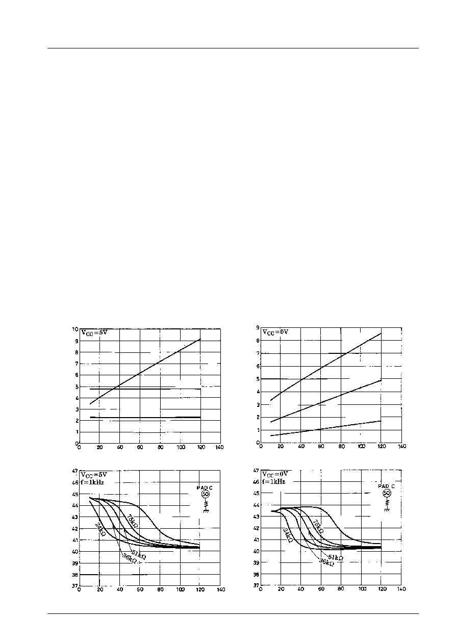
DC characteristics (power on)
DC characteristics (power off)
Pin 64
Pin 62
Pin 61
V
oltage
-
V
Line current, I
L
- mA
Pin 64
Pin 62
Pin 61
V
oltage
-
V
Line current, I
L
- mA
Transmitting characteristics (power on)
Transmitting characteristics (power off)
T
ransmitting
gain,
G
T
-d
B
Line current, I
L
- mA
Pin 56 input
Open
T
ransmitting
gain,
G
T
-d
B
Line current, I
L
- mA
Pin 56 input
Open
LA8518NM
No.5421-27/31
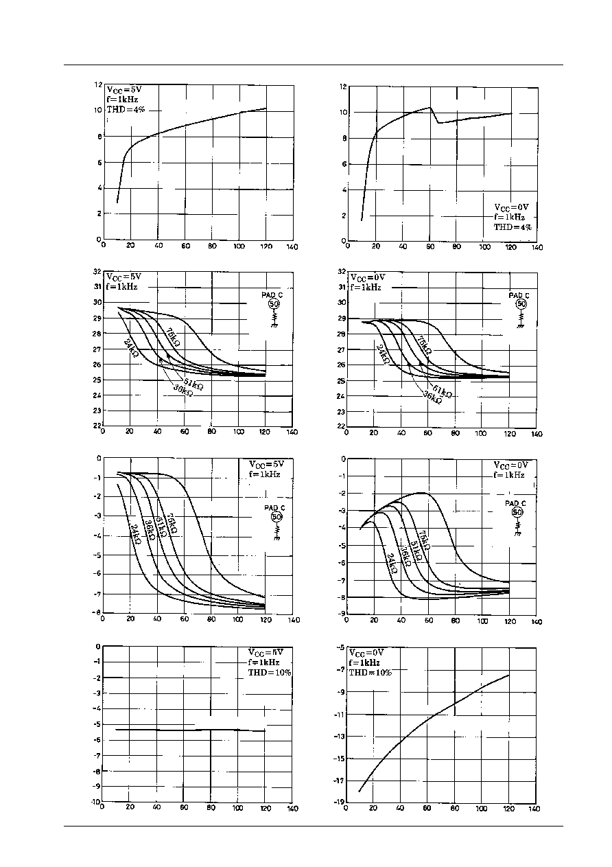
Transmitting dynamic range (power on)
Transmitting dynamic range (power off)
T
ransmitting
dynamic
range,
DR
T
-
dBV
Line current, I
L
- mA
Pin 56 input
Transmitting D range
T
ransmitting
dynamic
range,
DR
T
-
dBV
Line current, I
L
- mA
Pin 56 input
Transmitting D range
DTMF characteristics (power on)
DTMF characteristics (power off)
DTMF
gain,
G
MF
-d
B
Line current, I
L
- mA
Pin 60 input
Open
DTMF
gain,
G
MF
-d
B
Line current, I
L
- mA
Pin 60 input
Open
Receiving characteristics (power on)
Receiving characteristics (power off)
Receiving
gain,
G
R
-d
B
Line current, I
L
- mA
Pin 64 input
Open
Receiving
gain,
G
R
-d
B
Line current, I
L
- mA
Pin 64 input
Open
Receiving dynamic range (power on)
Receiving dynamic range (power off)
Receiving
dynamic
range,
DR
DR
-
dBV
Line current, I
L
- mA
Pin 64 input
Receiving D range
Receiving
dynamic
range,
DR
DR
-
dBV
Line current, I
L
- mA
Pin 64 input
Receiving D range
LA8518NM
No.5421-28/31

KT characteristics (power on)
KT
gain,
G
KT
-d
B
Line current, I
L
- mA
KT gain
Pin 55 input
KT characteristics (power off)
KT
gain,
G
KT
-d
B
Line current, I
L
- mA
KT gain
Pin 55 input
Quiescent current
Quiescent
current,
I
CCO
-m
A
Supply voltage, V
CC
- V
Quiescent current
V
REF
(Pin 30)
Reference
voltage,
V
REF
-V
Supply voltage, V
CC
- V
Equivalent input noise
Supply voltage, V
CC
- V
Equivalent
input
noise,
V
NI
-
�
V
rms
Each input shorting
PRE Amp ALC characteristics
Output
level,
V
O
-
m
V
rms
Input level - dBV
Output level
Pin 13 input
T
otal
harmonic
distortion,
THD
-
%
Address 34, 3C on
PB Amplifier input/output characteristics
Input level - dBV
Output
level,
V
O
-
m
V
rms
Pin 21 input
Address 3D on
Output level
T
otal
harmonic
distortion,
THD
-
%
PB Amplifier voltage gain
Frequency, f - Hz
V
oltage
gain,
VG
-
d
B
Gain
Pin 21 input
Address 3C on
LA8518NM
No.5421-29/31

OGM Amplifier input/output characteristics
Input level - dBV
Output
level,
V
O
-
m
V
rms
Output level
Pin 28 input
T
otal
harmonic
distortion,
THD
-
%
MIC Amp input/output characteristics
Pin 33 input
Output
level,
V
O
-
m
V
rms
T
otal
harmonic
distortion,
THD
-
%
Input level - dBV
Output level
Crosspoint switch output noise
Supply voltage, V
CC
- V
Output
noise,
V
NO
-
�
V
rms
Each input shorting
Pin 53
Pin 44
Pin 15
Crosspoint switch input characteristics
Output
level,
V
O
-
m
V
rms
Input level - dBV
T
otal
harmonic
distortion,
THD
-
%
Pin 13 input, Pin 18 output
Output level
Crosspoint switch crosstalk
Crosstalk,
CT
-
�
V
rms
Input level - dBV
Pin 13 input, Pin 18 output
Address 26 on
PB Amp (gain 50 dB)
PRE Amp
(gain 30 dB)
Receiving
amplifier
(gain 10 dB)
Pins 14,15,16,17,18
output
PWR Amplifier output noise
Output
noise,
V
NO
-
�
V
rms
Supply voltage, V
CC
- V
Input shorted
Noise
PWR Amp P
O
- THD characteristics
T
otal
harmonic
distortion,
THD
-
%
Output power, P
O
- mW
PWR Amplifier P
O
- V
CC
characteristics
Output
power
,
P
O
-m
W
Supply voltage, V
CC
- V
Output power
LA8518NM
No.5421-30/31

No products described or contained herein are intended for use in surgical implants, life-support systems, aerospace equipment,
nuclear power control systems, vehicles, disaster/crime-prevention equipment and the like, the failure of which may directly or
indirectly cause injury, death or property loss.
Anyone purchasing any products described or contained herein for an above-mentioned use shall:
1
Accept full responsibility and indemnify and defend SANYO ELECTRIC CO., LTD., its affiliates, subsidiaries and distributors
and all their officers and employees, jointly and severally, against any and all claims and litigation and all damages, cost and
expenses associated with such use:
2
Not impose any responsibility for any fault or negligence which may be cited in any such claim or litigation on SANYO
ELECTRIC CO., LTD., its affiliates, subsidiaries and distributors or any of their officers and employees jointly or severally.
Information (including circuit diagrams and circuit parameters) herein is for example only; it is not guaranteed for volume
production. SANYO believes information herein is accurate and reliable, but no guarantees are made or implied regarding its use
or any infringements of intellectual property rights or other rights of third parties.
This catalog provides information as of April, 1996. Specifications and information herein are subject to change without notice.
PWR Amp power dissipation characteristics
Output power - mW
Power
dissipation,
Pd
-
m
W
VOX sensitivity
Supply voltage, V
CC
- V
Input
level
-
dBV
Pin 36 input
VOX sensitivity resistance - ON level
ON
level
-
dBV
Resistance value -
ON level
Electronic volume control step width
V
oltage
gain,
VG
-
d
B
Level
Input -20 dBV
Series 1
VOX waveform shaping duty
Duty
-
%
Input level - dBV
Duty
Connect VOX, C pin to V
CC
LA8518NM
No.5421-31/31