 | –≠–ª–µ–∫—Ç—Ä–æ–Ω–Ω—ã–π –∫–æ–º–ø–æ–Ω–µ–Ω—Ç: LA8638V | –°–∫–∞—á–∞—Ç—å:  PDF PDF  ZIP ZIP |

Overview
The LA8638V provides dynamic range expansion, noise
suppression for enhancing the quality of audio signals in
cordless telephones and other communications systems.
This single chip provides the functions that make it ideal
for cordless telephones: a compressor with a logarithmic
compression ratio of 1/2, expander with a logarithmic
expansion ratio of 2, splatter filter, microphone amplifier,
BTL amplifier, waveform shaper for the receiving signal,
muting for both receiving and transmitting signals, and
standby operation.
Functions
∑ Transmitter circuits: compressor, microphone amplifier,
limiter (IDC), muting, output level changes to user-
specified levels, and splatter filter
∑ Receiver circuits: expander, buffer amplifier for filters,
muting, output level changes to user-specified levels,
and BTL amplifier
∑ Other circuits: waveform shaper for the receiving signal
and standby operation
Features
∑ Full processing of baseband signals for both receiving
and transmitting signals
∑ Built-in BTL receiver amplifier for driving a ceramic
speaker with a load of 2 k
∑ Standby operation that conserves battery power during
intermittent reception by disabling all but the waveform
shaper for the receiving signal
∑ Built-in splatter filter with user-specified fc
∑ Low-voltage operation (1.8 V to 5.5 V)
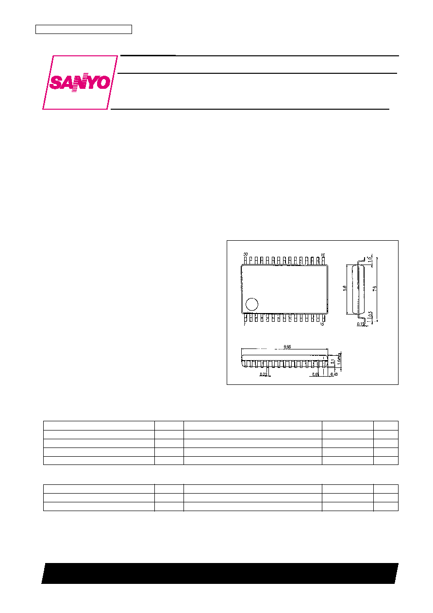
Package Dimensions
unit: mm
3191-SSOP30
Monolithic Linear IC
40398RM (OT) No. 5776-1/16
SANYO: SSOP30
[LA8638V]
SANYO Electric Co.,Ltd. Semiconductor Bussiness Headquarters
TOKYO OFFICE Tokyo Bldg., 1-10, 1 Chome, Ueno, Taito-ku, TOKYO, 110-8534 JAPAN
Low-voltage Compander IC
for Cordless Telephones
LA8638V
Ordering number : EN5776
Parameter
Symbol
Conditions
Ratings
Unit
Maximum power supply voltage
V
CC
max
7.0
V
Maximum power dissipation
Pd max
Ta
75∞C
100
mW
Operating temperature
Topr
≠20 to +75
∞C
Storage temperature
Tstg
≠40 to +125
∞C
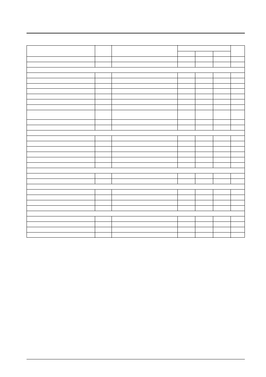
Specifications
Maximum Ratings
at Ta = 25∞C
Parameter
Symbol
Conditions
Ratings
Unit
Recommended power supply voltage
V
CC
2.4
V
Operating power supply voltage range
V
CC
op
1.8 to 5.5
V
Operating Conditions
at Ta = 25∞C

No. 5776-2/16
LA8638V
Parameter
Symbol
Conditions
Ratings
Unit
min
typ
max
Current drain with no signal
I
CCO
No signal
3.0
5.4
7.6
mA
Standby current
I
STBY
Standby mode, No signal
0.4
0.7
0.95
mA
[Transmitter block] V
inrefc
= ≠60 dBV = 0 dB, microphone amplifier gain = 40 dB, R
L
= 15 k
Output level
V
O
c
V
IN
= Vinrefc = 0 dB
≠18.1
≠16.1
≠14.1
dBV
Gain change level
G
C
c
V
IN
= ≠10 dB
3.5
4.0
4.4
dB
Gain error
G
E
c
V
IN
= ≠40 dB
≠2.0
≠0.7
+1.0
dB
Total harmonic distortion
THDc
V
IN
= 0 dB
0.45
1.0
%
Output noise voltage
V
NO
c
Rg = 620
, f = 20 to 20 kHz
1.8
4.5
mVrms
Limiting voltage
V
LT
V
IN
= +30 dB, 1 kHz BPF
0.88
1.05
1.23
Vp-p
Microphone amplifier maximum voltage gain
VG max
40
46
dB
Low pass filter attenuation
Lalt
f
IN
= 5 kHz; fifth-order Butterworth function
12.0
16.5
25.0
dB
filter (fc = 3.35 kHz)
Muting attenuation
ATTc
V
IN
= +30 dB, 1 kHz BPF
≠83
≠65
dBV
Crosstalk level
CTc
RX--V
IN
= ≠10 dBV, 1 kHz BPF
≠61
≠50
dBV
[Receiver block] V
inrefe
= ≠20 dBV = 0 dB, R
L
= 15 k
Output level
V
O
e
V
IN
= V
inrefe
= 0 dB
≠18.8
≠16.3
≠13.8
dBV
Gain change level
G
C
e
V
IN
= 0 dB
6.0
7.1
8.4
dB
Gain error
G
E
e
V
IN
= ≠30 dB
≠1.5
+0.3
+2.0
dB
Output noise voltage
V
NO
e
Rg = 620
, f = 20 to 20 kHz
50
100
µVrms
Muting attenuation
ATTe
V
IN
= +10 dB, 1 kHz BPF
≠100
≠80
dBV
Crosstalk level
CTe
TX--V
IN
= ≠40 dBV, 1 kHz BPF
≠83
≠65
dBV
[BTL amplifier] R
L
= 2 k
Maximum output voltage
V
O
btl
THD = 3%
3.2
4.2
Vp-p
Total harmonic distortion
THDbtl
V
IN
= ≠5 dBV
0.4
1.0
%
[Data shaper] V
IN
= ≠20 dBV, R
L
= 100 k
Duty factor
DUTY
43
50
57
%
Dead zone
UNSN
≠39.0
≠34.5
≠30.0
dBV
Output "H" level
V
H
2.2
2.38
V
Output "L" level
V
L
0.12
0.3
V
[Digital input characteristics]
Input "H" level 1
V
IH
1
Pins 17, 18, 20, and 22
0.6 V
CC
V
Input "L" level 1
V
IL
2
Pins 17, 18, 20, and 22
0.25 V
CC
V
Input "H" level 2
V
IH
2
Pin 19
1.3
V
Input "L" level 2
V
IL
2
Pin 19
0.3
V
Electrical Characteristics
at Ta = 25∞C, V
CC
= 2.4 V, f
IN
= 1 kHz

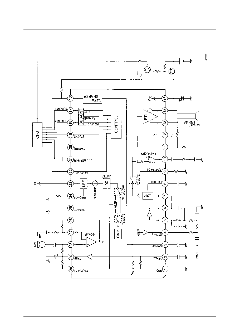
Block Diagram
No. 5776-3/16
LA8638V

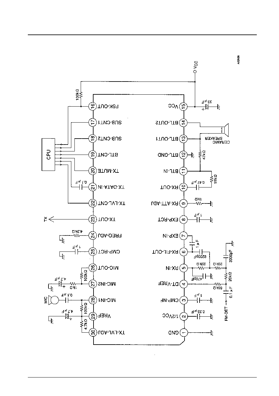
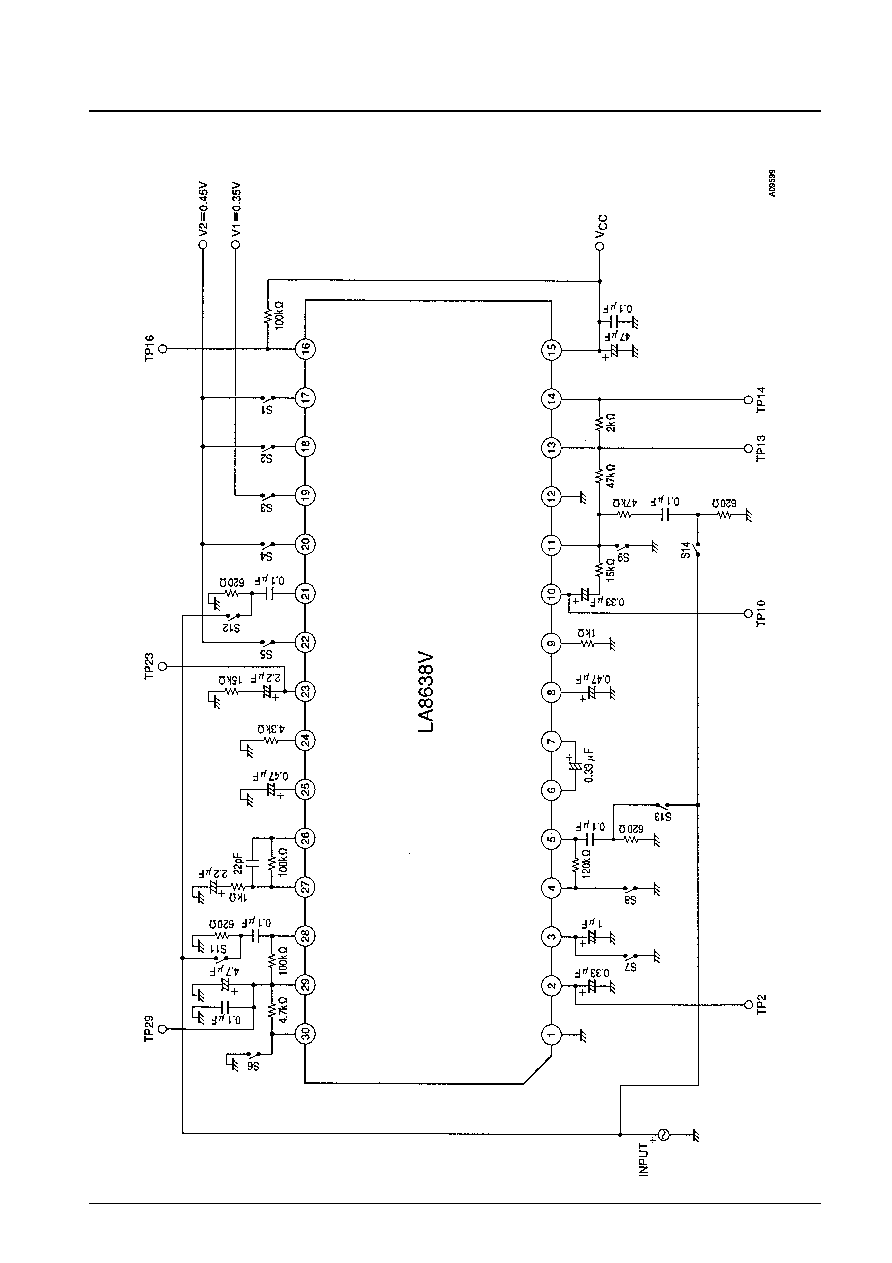
Sample Application Circuit
No. 5776-4/16
LA8638V

Test Circuit
No. 5776-5/16
LA8638V

Usage Notes
1. Internal Reference Voltages
The chip uses the following reference voltages internally.
Pin 29 (V
REF
) Power supply voltage follower (approximately 0.5 V
CC
)
Pin 4 (V
REF
2) Fixed voltage (approximately 1.25 V)
2. Microphone Amplifier
Do not use the microphone amplifier as a buffer amplifier (non-reversing, zero-gain amplifier) because it is designed
for high-gain operation--that is, gains above 6 dB--and is susceptible to oscillation below that level.
For proper circuit balance, use the same resistance value for the bias resistor (between pins 28 and 29) and the
feedback resistor (between pins 26 and 27).
3. BTL Amplifier
The built-in BTL amplifier is designed for ceramic speakers only. Do not use it to drive a dynamic speaker.
4. Receiver Input Filter
The receiver input filter uses external capacitors and resistors to determine the cutoff frequencies. The external circuit
constants may be easily derived from the standardized circuit constants. Start by making all resistors the same size
and determine the capacitances required to achieve the desired cutoff frequencies from the circuit constants in Table
1. Then, because capacitors are not available for such precise values, choose the closest ones available and then fine-
tune the resistances. (As a result, the final resistances will not necessarily be equal.)
Once the filter constants have been established, choose the bias voltage supply resistor R
B
so that the total DC
resistance between pins 4 and 5 is on the order of 120 k
to standardize the voltage drop across this path due to the
small base current from the transistor in the pin 5 input circuit and thus the duty factor for the data shaper at the next
stage.
5. Splatter Filter Cutoff Frequency
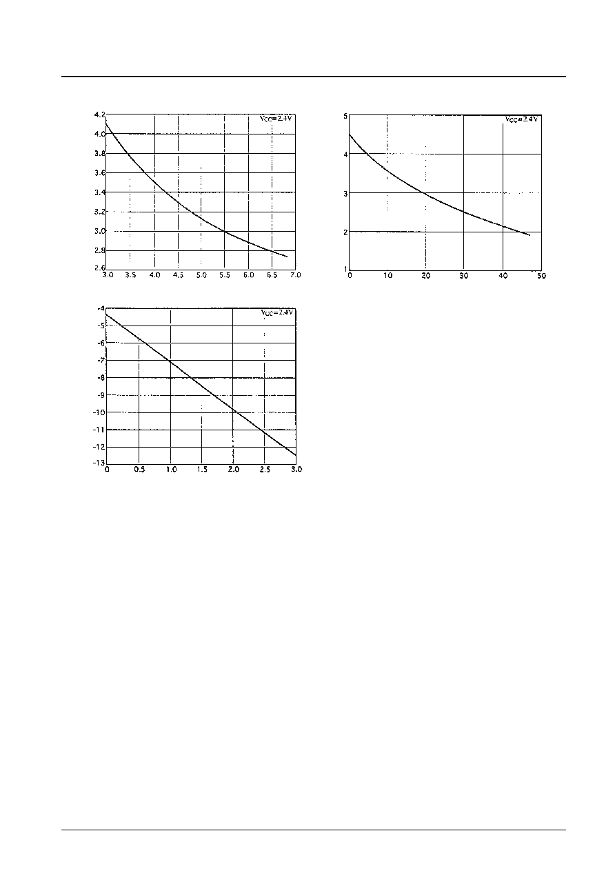
The resistance between pin 24 and ground determines the cutoff frequency for the splatter filter in the transmitter
circuit. (See Graph 1 on p. 8.) To fine-tune this frequency, use two resistors and adjust them to achieve the desired
frequency.
6. Gain Change Levels
The resistance between pins 29 and 30 determines the gain change level for the transmitter circuits. (See Graph 2
on p. 8.)
The resistance between pin 9 and ground determines the gain change level for the receiver circuits. (See Graph 3
on p. 8.)
No. 5776-6/16
LA8638V
Table 1. Standardized Circuit Constants
The Bessel functions for cutoff frequencies do not incorporate the notion of 3-
dB attenuation. The 3-dB attenuation frequency for the second-order function
is 1.38 fc; for the third-order function, 1.75 fc.
Lowpass filter type
X1
X2
X3
Second-order Butterworth function
0.7071
1.4142
--
Third-order Butterworth function
0.2025
3.5468
1.3926
Second-order Bessel function
0.5000
0.6667
--
Third-order Bessel function
0.1451
0.8136
0.5647

7. Protective Diodes Preventing Static Breakdown
The control pins and data output pins have had their upper protective diodes removed so as to permit direct
connection to a microcomputer.
No protective diodes:
V
CC
(pin 15), GND (pins 1 and 12)
Lower protective diodes only:
Pins 16 to 20, 22
Both upper and lower protective diodes: All other pins
8. Preemphasis and Deemphasis
This chip provides preemphasis in the microphone amplifier and deemphasis in the BTL amplifier's input stage. The
amount depends on the CR time constants for the filters on the corresponding pins--the primary high pass filter on
the microphone amplifier's positive (pin 28) or negative (pin 27) input for preemphasis and the primary low pass filter
between pins 10 and 11 for deemphasis.
9. Full-Wave Rectifier Smoothing Capacitors
The external capacitors on pins 8 and 25 are for the full-wave rectifiers for the expander and compressor. They not
only smooth the output but also determine the time constant for the transient characteristics. This time constant is the
product of the capacitance and 15 k
, the input resistance of the full-wave rectifier. Although there is a tendency to
lower the time constant for the expander to reduce noise at the ends of words, the designer must keep in mind that
such cuts reduce the amount of smoothing and thus raise the risk of distortion.
10. Compressor's Summing Amplifier
Achieving a DC gain of 1 and an AC gain of infinity from the compressor's summing amplifier requires suppressing
AC feedback with the capacitor on pin 3. The cutoff frequency is determined by the product of its capacitance and the
internal resistance of 22.5 k
.
11. Standby Function
The chip's standby function does not produce a total shutdown of all circuits. It disables the audio signal processing
block, but leaves the waveform shaper block for the receiving signal operating. For this reason, it is not possible to
connect the battery directly to the power supply pin (pin 15). There must be an intervening transistor switch for an
intermittent power supply.
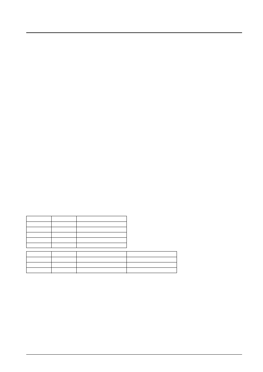
12. Control Modes
No. 5776-7/16
LA8638V
Pin 17
Pin 18
SUB-CNT1
SUB-CNT2
Mode
OPEN/HIGH
OPEN/HIGH
Standby
OPEN/HIGH
LOW
Receiver muted
LOW
OPEN/HIGH
Normal receiver output levels
LOW
LOW
Low receiver output levels
Pin Number
Pin Name
OPEN/HIGH
LOW
Pin 19
BTL-CNT
BTL amplifier disabled
BTL amplifier enabled
Pin 20
TX-MUTE
Transmitter muted
Transmitter enabled
Pin 22
TX-LVL-CNT
Normal transmitter output levels
High transmitter output levels
Note: The standby mode overrides all other mode settings.

No. 5776-8/16
LA8638V
Graph 1. Splatter Filter Cutoff Frequency vs. External Resistance
Graph 2. Transmitter Gain Change Level vs. External Resistance
Graph 3. Receiver Gain Change Level vs. External Resistance
External resistance (k
)
Cutoff frequency (kHz)
Level difference (dB)
Level difference (dB)
External resistance (k
)
External resistance (k
)

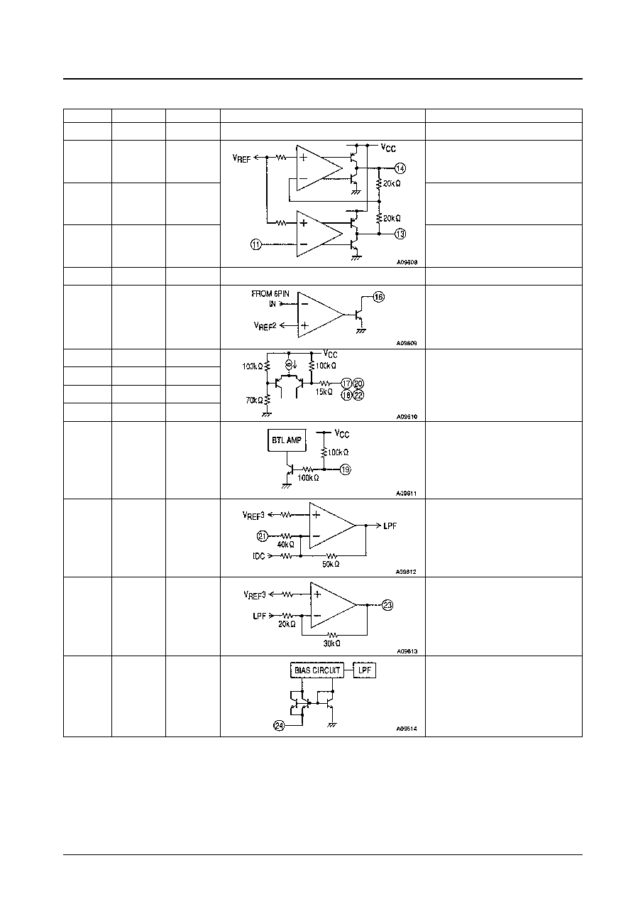
Pin Number
Pin Name
Pin Voltage
Equivalent Circuit
Description
No. 5776-9/16
LA8638V
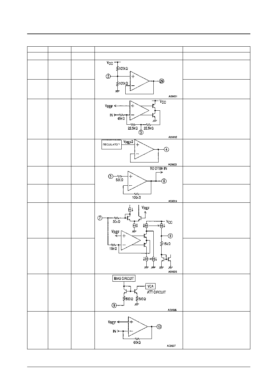
Pin Descriptions
1
GND
Ground for all circuits except BTL amplifier
2
1/2 V
CC
V
CC
/2
Resistance voltage divider pin
29
V
REF
V
CC
/2
Reference voltage for all circuits except
receiver block
3
CMP-NF
V
CC
/2
AC feedback control for compressor's
summing amplifier DC gain: 1 AC gain:
Infinite
4
DT-V
REF
1.25 V
Reference voltage for receiver block This
supplies the bias voltage for pin 5.
5
RX-IN
1.25 V power
supply
Filter buffer input
6
RX-FIL-OUT
1.25 V
Filter buffer output
7
EXP-IN
V
CC
/2
Expander input. Voltage-current converter
input. Full-wave rectifier input.
8
EXP-RCT
Indeterminate
(when there is
no signal)
Full-wave rectifier output for expander block
(AC smoothing)
9
RX-ATT-ADJ
0.03 V
Pin for setting attenuation for receiver output
level switching
10
RX-OUT
V
CC
/2
Receiver block output
Continued on next page.

No. 5776-10/16
LA8638V
Continued from preceding page.
Pin Number
Pin Name
Pin Voltage
Equivalent Circuit
Description
12
BTL-GND
Ground for BTL amplifier
11
BTL-IN
V
CC
/2
BTL amplifier input
13
BTL-OUT1
V
CC
/2
BTL amplifier reversed output
14
BTL-OUT2
V
CC
/2
BTL amplifier non-reversed output
15
V
CC
Power supply pin
16
FSK-OUT
Indeterminate
(when there is
no signal)
Comparator output (open collector output)
17
SUB-CNT1
V
CC
Internal operating mode control pins. All four
have identical structures.
18
SUB-CNT2
V
CC
20
TX-MUTE
V
CC
22
TX-LVL-CNT
V
CC
19
BTL-CNT
V
CC
+ 0.65
----------
2
BTL amplifier operation control pins
21
TX-DATA-IN
V
CC
/1.6
Transmitter data input
23
TX-OUT
V
CC
/1.6
Transmitter output
24
FREQ-ADJ
0.01 V
Pin for setting cutoff frequency of splatter
filter
Continued on next page.

No. 5776-11/16
LA8638V
Continued from preceding page.
Pin Number
Pin Name
Pin Voltage
Equivalent Circuit
Description
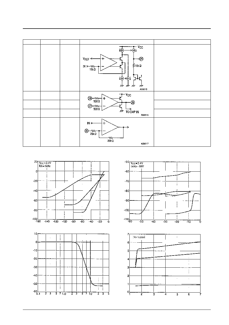
25
CMP-RCT
Full-wave rectifier output for compressor
block (AC smoothing)
Indeterminate
(when there is
no signal)
26
MIC-OUT
Microphone amplifier output
V
CC
/2
30
TX-LVL-ADj
Pin for setting amplification for transmitter
output level switching
V
CC
/2
27
MIC-IN2
Microphone amplifier negative input
V
CC
/2
28
MIC-IN1
Microphone amplifier positive input
V
CC
/2 power
supply
I/O Characteristics
Crosstalk Characteristics
Input level, V
IN
-- dBV
Splatter Filter Frequency Characteristics
Input level, V
IN
-- dBV
Current Drain --. V
CC
Frequency, f -- kHz
Power supply voltage, V
CC
-- V
Output level, V
O
-- dBV
Response -- dB
Crosstalk level, CT -- dBV
Current drain, I
CC
--
mA
V
CC
= 2.4 V; resistance
TX-OUT (pin 23)
TX-DT-OUT (pin 23)
RX-OUT (pin 10)
RX
TX (pin 23)
TX-MUTE (pin 23)
TX
RX (pin 10)
RX-MUTE (pin 10)
BTL on
BTL off
Standby

No. 5776-12/16
LA8638V
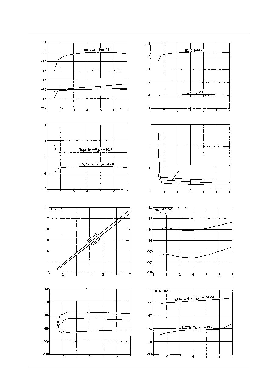
Output Level
--
V
CC
Gain Change Level Difference
--
V
CC
Power Supply Voltage, -- V
CC
V
Compander Gain Error
--
V
CC
Power supply voltage, V
CC
-- V
Output Distortion
--
V
CC
Power supply voltage, V
CC
-- V
Power supply voltage, V
CC
-- V
BTL Power Amplifier Maximum Output Voltage
--
V
CC
Receiver Muting Attenuation
--
V
CC
Power supply voltage, V
CC
-- V
Receiver (TX
RX) Crosstalk
--
V
CC
Power supply voltage, V
CC
-- V
Transmitter Crosstalk
--
V
CC
Power supply voltage, V
CC
-- V
Power supply voltage, V
CC
-- V
Output level, V
O
-- dBV
Gain change level difference, GC -- dB
Compander gain error, GE -- dB
Total harmonic distortion, THD -- %
Maximum output voltage, V
O
-- Vp-p
Muting level -- dBV
Crosstalk level, CT -- dBV
Crosstalk level, CT -- dBV
TX (pin 23)
V
IN
= ≠60 dBV
RX (pin 10)
V
IN
= ≠20 dBV
RX (pin 10)
V
IN
= ≠20 dBV
TX (pin 23)
V
IN
= ≠60 dBV
TX-DATA (pin 23)
V
IN
= ≠20 dBV
Switches gain between high and low levels.
Resistance at pin 9: 1 k
; Resistance
between pins 30 and 29: 4.7 k
Pins 13 and 14
Pin 10
Pin 13
Pin 10
Pin 14
1 kHz-BPF
TX-IN(28 pin): V
IN
= ≠40dBV

No. 5776-13/16
LA8638V
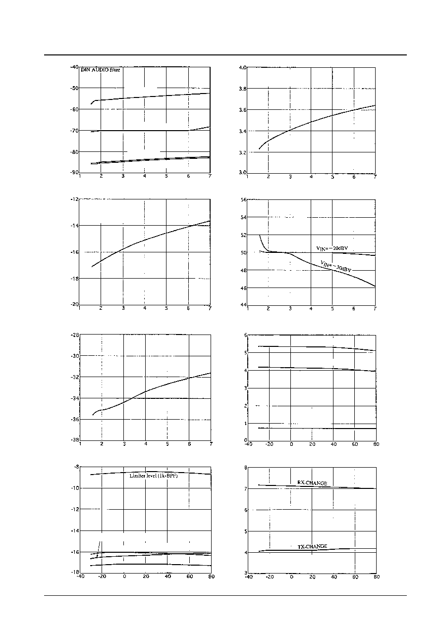
Output Noise Level
--
V
CC
Splatter Filter Cutoff Frequency
--
V
CC
Power supply voltage, V
CC
-- V
Splatter Filter Attenuation
--
V
CC
Power supply voltage, V
CC
-- V
Data Shaper Duty Cycle
--
V
CC
Power supply voltage, V
CC
-- V
Data Shaper Dead Zone
--
V
CC
Power supply voltage, V
CC
-- V
Current Drain
--
Ta
Power supply voltage, V
CC
-- V
Output Level
--
Ta
Ambient temperature, Ta
--
∞C
Gain Change Level Difference
--
Ta
Ambient temperature, Ta
--
∞C
Ambient temperature, Ta
--
∞C
Output level, V
O
-- dBV
Gain change level difference, GC -- dB
Current drain, I
CC
-- mA
Minimum input level -- dBV
Duty cycle -- %
Cutoff frequency -- kHz
Output noise level -- dBV
Attenuation -- dB
TX (pin 23)
TX (pin 23)
TX (pin 23)
f
IN
= 5 or 1 kHz;
resistance at pin 24
= 4.3 k
Att. = 3 dB down;
resistance at pin 24
= 4.3 k
BTL on
BTL off
Standby
RX (pin 10)
V
IN
= ≠20 dBV
TX (pin 23)
V
IN
= ≠60 dBV
TX-DATA (pin 23)
V
IN
= ≠20 dBV
Switches gain between high and low levels.
Resistance at pin 9: 1 k
; Resistance
between pins 30 and 29: 4.7 k
No signal

No. 5776-14/16
LA8638V
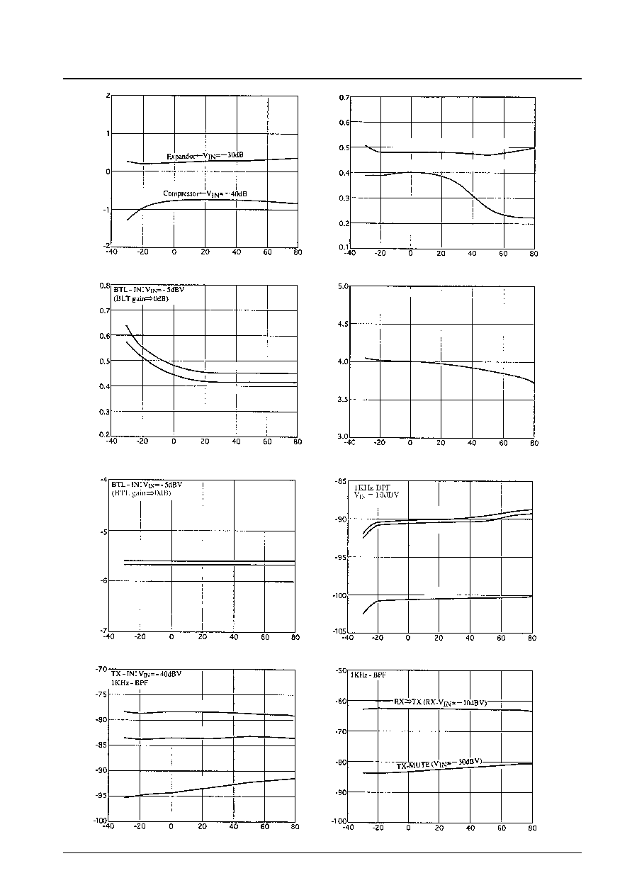
Compander Gain Error
--
Temperature
Output Distortion
--
Temperature
BTL Distortion
--
Temperature
BTL Power Amplifier Maximum Output Voltage
--
Temperature
Ambient temperature, Ta -- ∞C
Ambient temperature, Ta -- ∞C
Ambient temperature, Ta -- ∞C
BTL Output Level
--
Temperature
Ambient temperature, Ta -- ∞C
Receiver Muting Attenuation
--
Temperature
Ambient temperature, Ta -- ∞C
Receiver (TX
RX) Crosstalk
--
Temperature
Ambient temperature, Ta -- ∞C
Transmitter Crosstalk
--
Temperature
Ambient temperature, Ta -- ∞C
Ambient temperature, Ta -- ∞C
Crosstalk level, CT -- dBV
Crosstalk level, CT -- dBV
Muting level -- dBV
Output level, V
O
-- dBV
Total harmonic distortion, THD -- %
Maximum output voltage, V
O
-- V
PP
Total harmonic distortion, THD -- %
Compander gain error, GE -- dB
Pin 13
Pin 10
Pin 14
Pin 13
Pin 14
Pin 14
Pin 13
Pin 10
Pin 13
Pin 14
TX (pin 23)
V{IN} = ≠60 dBV
RX (pin 10)
V{IN} = ≠20 dBV
THD output = 1 %

No. 5776-15/16
LA8638V
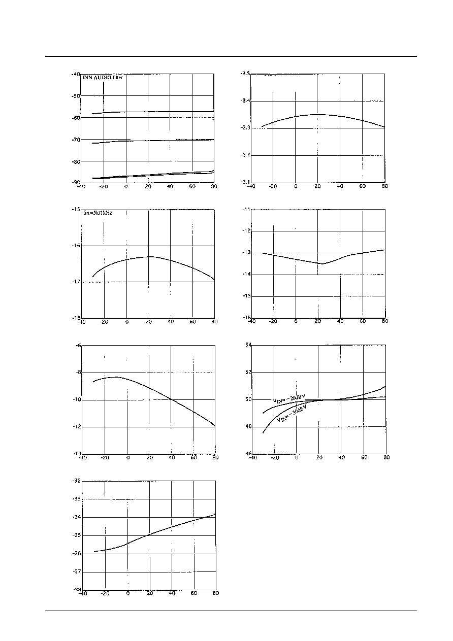
Output Noise Level
--
Temperature
Splatter Filter Cutoff Frequency
--
Temperature
Ambient temperature, Ta -- ∞C
Splatter Filter Attenuation
--
Temperature
Ambient temperature, Ta -- ∞C
Receiver Maximum Input Level
--
Temperature
Ambient temperature, Ta -- ∞C
Transmitter Maximum Input Level
--
Temperature
Ambient temperature, Ta -- ∞C
Data Shaper Duty Cycle
--
Temperature
Ambient temperature, Ta -- ∞C
Ambient temperature, Ta -- ∞C
Data Shaper Dead Zone
--
Temperature
Ambient temperature, Ta -- ∞C
Minimum input level -- dBV
Duty cycle -- %
Maximum input level at pin 21 -- dBV
Maximum inputlevel at pin 5 -- dBV
Cutoff frequency -- kHz
Attenuation
--
dB
Output noise level -- dBV
THD = 1% for output from pin 23
TX (pin 23)
TX-MUTE (pin 23)
RX (pin 10)
Att. = 3 dB down;
resistance at pin
24 = 4.3 k
THD = 1% for
output from pin 10
RX-MUTE (pin 10)

PS No. 5776-16/16
LA8638V
This catalog provides information as of April, 1998. Specifications and information herein are subject to change
without notice.
s
No products described or contained herein are intended for use in surgical implants, life-support systems, aerospace
equipment, nuclear power control systems, vehicles, disaster/crime-prevention equipment and the like, the failure of
which may directly or indirectly cause injury, death or property loss.
s
Anyone purchasing any products described or contained herein for an above-mentioned use shall:
Accept full responsibility and indemnify and defend SANYO ELECTRIC CO., LTD., its affiliates, subsidiaries and
distributors and all their officers and employees, jointly and severally, against any and all claims and litigation and all
damages, cost and expenses associated with such use:
Not impose any responsibility for any fault or negligence which may be cited in any such claim or litigation on
SANYO ELECTRIC CO., LTD., its affiliates, subsidiaries and distributors or any of their officers and employees
jointly or severally.
s
Information (including circuit diagrams and circuit parameters) herein is for example only; it is not guaranteed for
volume production. SANYO believes information herein is accurate and reliable, but no guarantees are made or implied
regarding its use or any infringements of intellectual property rights or other rights of third parties.
