
Analog Signal Processor (ASP)
for CD players
Overview
The LA9240M is an analog signal processing and servo control
bipolar IC designed for use in compact disc players; a compact
disc player can be configured by combining this IC with a
CD-DSP such as the LC78622E and LC78620E, with a small
number of additional components required.
Functions
I/V amplifier, RF amplifier (with AGC), SLC, APC, FE, TE
(with VCA and auto-balance function), focus servo amplifier
(with offset cancellation function), tracking servo amplifier
(with offset cancellation function), spindle servo amplifier
(with gain switching function), sled servo amplifier (with off
function), focus detection (DRF, FZD), track detection (HFL,
TES), defect detection, and shock detection.
Features
.
The following automatic adjustment functions are built in.
.
Focus offset auto cancel: FE (pin 20)
.
Tracking offset auto cancel: TE (pin 7)
.
EF balance auto adjustment
.
RF level AGC function
.
Tracking servo gain RF level following function
.
Focus search smoothing setting pin: FSC (pin 46)
.
EF balance adjustment variable range setting pin: TBC (pin
47)
.
Focus search mode switching pin: FSS (pin 55)
Package Dimensions
unit : mm
3159-QFP64E
[LA9240M]
SANYO : QIP64E
Specifications
Maximum Ratings
at Ta = 25�C, Pins 22, 45 = GND
Parameter
Symbol
Conditions
Ratings
Unit
Maximum supply voltage
V
CC
max
Pin 56, 64
7
V
Allowable power dissipation
Pd max
350
mW
Operating temperature
Topr
�25 to +75
�C
Storage temperature
Tstg
�40 to +150
�C
Ordering number: EN 5482A
Monolithic Linear IC
LA9240M
SANYO Electric Co.,Ltd. Semiconductor Bussiness Headquarters
TOKYO OFFICE Tokyo Bldg., 1-10, 1 Chome, Ueno, Taito-ku, TOKYO, 110 JAPAN
83097HA(II)/83096HA(II) No.5482 - 1/20
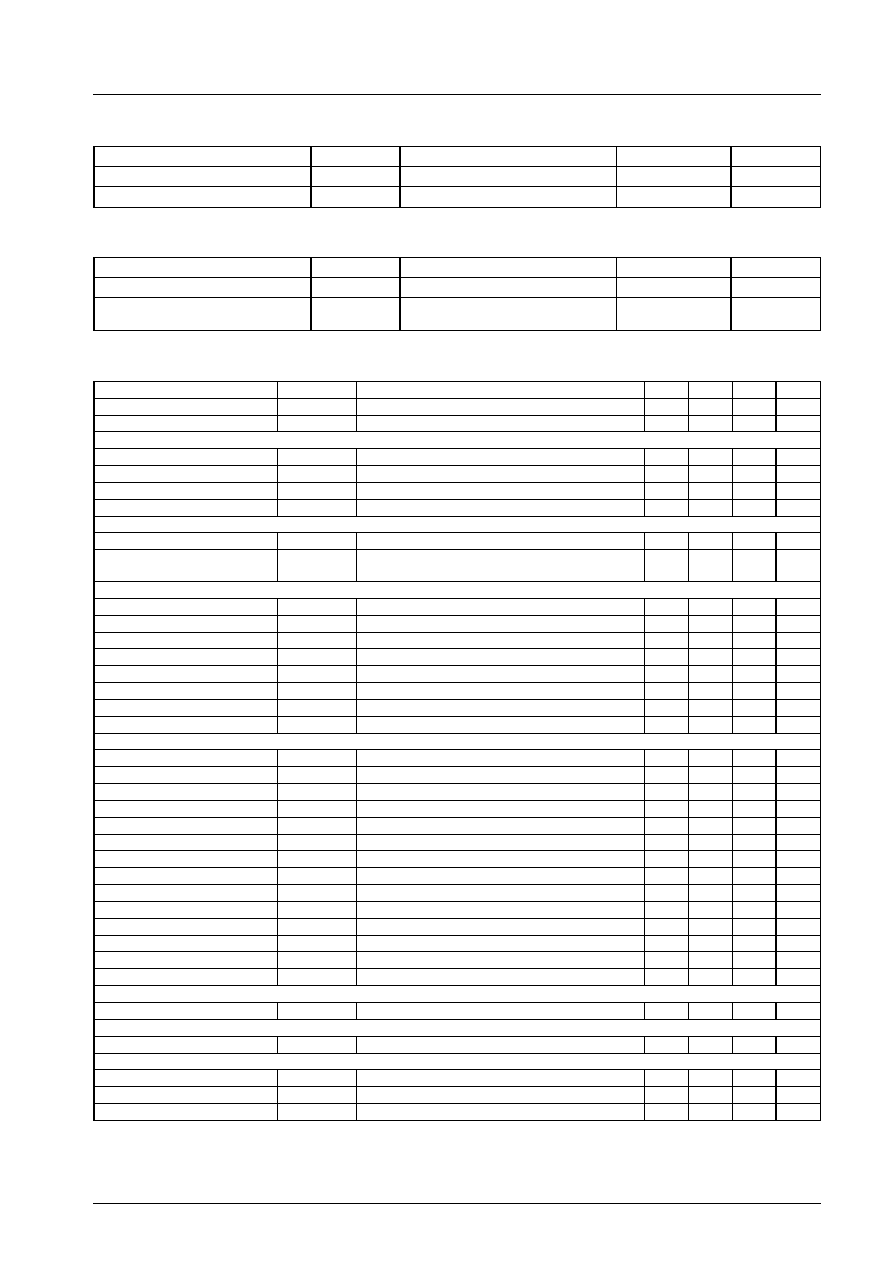
Operating Conditions
at Pins 22, 45 = GND
Parameter
Symbol
Conditions
Ratings
Unit
Recommended supply voltage
V
CC
5
V
Operating supply voltage
V
CC
op
3.6 to 5.5
V
*
Operating Supply Voltage at Limit of Operating Temperature
at Pins 22, 45 = GND
Parameter
Symbol
Conditions
Ratings
Unit
Operating temperature
Topr2
�5 to +75
�C
Operating supply voltage
V
CC
op2
Set resistance R between DSP and
CLK interface to 5.1 k
3.4 to 5.5
V
Operating Characteristics
at Ta = 25�C, Pins 22, 45 = GND, V
CC
(pins 56, 64) = 5 V
Parameter
Symbol
Conditions
min
typ
max
Unit
Current drain
I
CCO
V
CC
1 (pin 64) + V
CC
2 (pin 56)
22
32
42
mA
Reference voltage
V
REF
VR
2.3
2.5
2.7
V
[Interface]
CE-Vth
CEvth
CE
0.8
V
CL-Vth
CLvth
CL
0.8
V
DAT-Vth
DATvth
DAT
0.8
V
Maximum CL frequency
CLmax
500
kHz
[RF amplifier]
RFSM no signal voltage
RFSMo
1.35
1.60
1.85
V
Minimum gain
RFSM
G
min
FIN1, FIN2 : 1 M
-input, PH1 = 4 V
freq = 200 kHz, RFSM
�14.0
�12.5
�11.0
dB
[Focus amplifier]
FDO gain
FD
G
FIN2 : 1 M
-input, FDO
3.5
5.0
6.5
dB
FDO offset
FDost
Difference from reference voltage, servo on
�170
0
+170
mV
Off time offset
FDofost
Difference from reference voltage, servo off
�40
0
+40
mV
Offset adjustment step
FEstep
FE
3
mV
F search voltage H1
FSmax1
FDO, FSS = GND
0.8
V
F search voltage L1
FSmin1
FDO, FSS = GND
�0.8
V
F search voltage H2
FSmax2
FDO, FSS = V
CC
0.8
V
F search voltage L2
FSmin2
FDO, FSS = V
CC
0
V
[Tracking amplifier]
TE gain MAX
TE
G
max
f = 10 kHz, E: 1 M
-input, PH1 = 4 V
6.0
7.5
9.0
dB
TE gain MIN
TE
G
min
f = 10 kHz, E: 1 M
-input, PH1 = 1 V
�0.5
+1.8
+4.0
dB
TE-3 dB
TEfc
E: 1 M
-input
60
kHz
TO gain
TO
G
TH
TO gain, THLD mode
4.0
6.0
8.0
dB
TGL offset
TGLost
Servo on, TGL = H, TO
�250
0
+250
mV
TGH offset
TGHost
TGL = L, difference from TGL offset, TO
�50
0
+50
mV
THLD offset
THLDost
THLD mode, difference from TGL offset, TO
�50
0
+50
mV
Off 1 offset
OFF1ost
TOFF = H
�50
0
+50
mV
Off 2 offset
OFF2ost
TOFF2 off (IF)
�50
0
+50
mV
Offset adjustment step
TEstep
TE
30
mV
Balance range H
BAL-H
Gain E/F input, TB = 5 V, TBC = open
3.5
dB
Balance range L
BAL-L
Gain E/F input, TB = 0 V, TBC = open
�3.5
dB
TOFF-VTH
TOFFvth
1.0
2.5
3.0
V
TGL-VTH
TGLvth
1.0
2.5
3.0
V
[PH]
No signal voltage
PHo
Difference from RFSM
�0.85
�0.65
�0.45
V
[BH]
No signal voltage
BHo
Difference from RFSM
0.45
0.65
0.85
V
[DRF]
Detection voltage
DRFvth
Difference from VR at RFSM
�0.60
�0.35
�0.20
V
Output voltage H
DRF-H
4.5
4.9
V
Output voltage L
DRF-L
0
+0.5
V
Continued on next page.
LA9240M
No.5482 - 2/20
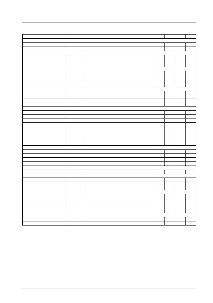
Continued from preceding page.
Parameter
Symbol
Conditions
min
typ
max
Unit
[FZD]
Detection voltage 1
FZD1
FE, difference from VR
0
+0.2
V
Detection voltage 2
FZD2
FE, difference from VR
0
V
[HFL]
Detection voltage
HFLvth
Difference from VR at RFSM
�0.55
�0.4
�0.25
V
Output voltage H
HFL-H
4.5
4.9
Output voltage L
HFL-L
0
+0.5
V
[TES]
Detection voltage LH
TES-LH
TESI, difference from VR
�0.15
�0.10
�0.05
V
Detection voltage HL
TES-HL
TESI, difference from VR
0.05
0.10
0.15
V
Output voltage H
TES-H
4.5
4.9
V
Output voltage L
TES-L
0
+0.5
V
[JP]
Output voltage H
JP-H
Difference from JP
+
= 0 V, JP
�
= 0 V at JP
+
= 0 V,
JP
�
= 5 V, TO
0.35
0.5
0.65
V
Output voltage L
JP-L
Difference from JP
+
= 0 V, JP
�
= 0 V at JP
+
= 5 V,
JP
�
= 0 V, TO
�0.65
�0.5
�0.35
V
[Spindle amplifier]
Offset 12
SPD12ost
Difference from VR at SPD, 12 cm mode
�40
0
+40
mV
Offset 8
SPD8ost
Difference from VR at SPD, 8 cm mode
�40
0
+40
mV
Offset off
SPDof
Difference from VR at SPD, OFF mode
�30
0
+30
mV
Output voltage H12
SPD-H12
Difference from offset-12, 12 cm mode
CV
+
= 5 V, CV
�
= 0 V
0.75
1.0
1.25
V
Output voltage L12
SPD-L12
Difference from offset-12 , 12 cm mode
CV
+
= 0 V, CV
�
= 5 V
�1.25
�1.0
�0.75
V
Output voltage H8
SPD-H8
Difference from offset-8, 8 cm mode
CV
+
= 5 V, CV
�
= 0 V
0.35
0.5
0.65
V
[Sled amplifier]
SLEQ offset
SLEQost
Difference from TO at SLEQ
�30
0
+30
mV
Offset SLD
SLDost
SLEQ = VR, Difference from VR
�100
0
+100
mV
Offset off
SLDof
Off mode
�40
0
+40
mV
Off VTH
SLOFvth
SLOF
1.0
1.4
2.0
V
[SLC]
No signal voltage
SLCo
SLC
2.25
2.5
2.75
V
[Shock]
No signal voltage
SCIo
SCI, difference from VR
�40
0
+40
mV
Detection voltage H
SCIvthH
SCI, difference from VR
60
100
140
mV
Detection voltage L
SCIvthL
SCI, difference from VR
�140
�100
�60
mV
[DEF]
Detection voltage
DEFvth
Difference between LF2 voltage when RFSM =
3.5 V and DEF is detected and LF2 voltage when
RFSM = 3.5 V
0.20
0.35
0.50
V
Output voltage H
DEF-H
4.5
4.9
V
Output voltage L
DEF-L
0
+0.5
V
[APC]
Reference voltage
LDS
LDS voltage at which LDD = 3 V
150
180
210
mV
Off voltage
LDDof
LDD
3.9
4.3
4.6
V
LA9240M
No.5482 - 3/20
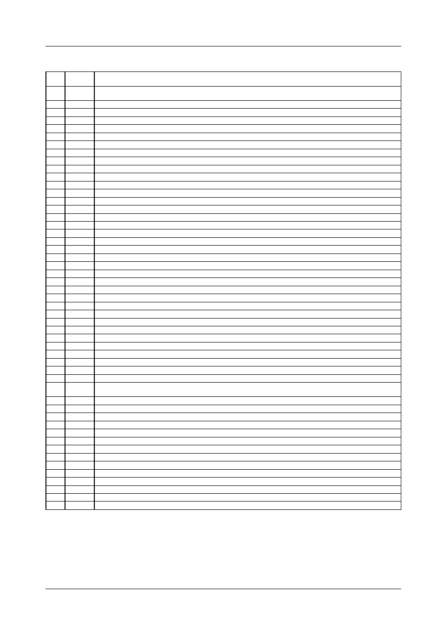
Pin Functions
Pin
No.
Symbol
Contents
1
FIN2
Pickup photodiode connection pin. Added to FIN1 pin to generate the RF signal, subtracted from FIN1 pin to generate
the FE signal.
2
FIN1
Pickup photodiode connection pin.
3
E
Pickup photodiode connection pin. Subtracted from F pin to generate the TE signal.
4
F
Pickup photodiode connection pin.
5
TB
TE signal DC component input pin.
6
TE
-
Pin which connects the TE signal gain setting resistor between this pin and TE pin.
7
TE
TE signal output pin.
8
TESI
TES (Track Error Sense) comparator input pin. The TE signal is input through a bandpass filter.
9
SCI
Shock detection input pin.
10
TH
Tracking gain time constant setting pin.
11
TA
TA amplifier output pin.
12
TD
-
Pin for configuring the tracking phase compensation constant between the TD and VR pins.
13
TD
Tracking phase compensation setting pin.
14
JP
Tracking jump signal (kick pulse) amplitude setting pin.
15
TO
Tracking control signal output pin.
16
FD
Focusing control signal output pin.
17
FD
-
Pin for configuring the focusing phase compensation constant between the FD and FA pins.
18
FA
Pin for configuring the focusing phase compensation constant between the FD
-
and FA
-
pins.
19
FA
-
Pin for configuring the focusing phase compensation constant between the FA and FE pins.
20
FE
FE signal output pin.
21
FE
-
Pin which connects the FE signal gain setting resistor between this pin and FE pin.
22
AGND
Analog signal GND.
23
SP
CV
+
and CV
-
pins input signal single-end output.
24
SPI
Spindle amplifier input.
25
SPG
12-cm spindle mode gain setting resistor connection pin.
26
SP
-
Spindle phase compensation constant connection pin, along with the SPD pin.
27
SPD
Spindle control signal output pin.
28
SLEQ
Sled phase compensation constant connection pin.
29
SLD
Sled control signal output pin.
30
SL
-
Input pin for sled movement signal from microprocessor.
31
SL
+
Input pin for sled movement signal from microprocessor.
32
JP
-
Input pin for tracking jump signal from DSP.
33
JP
+
Input pin for tracking jump signal from DSP.
34
TGL
Input pin for tracking gain control signal from DSP. Gain is low when TGL is high.
35
TOFF
Input pin for tracking off control signal from DSP. Tracking servo is off when TOFF is high.
36
TES
Output pin for TES signal to DSP.
37
HFL
The High Frequency Level is used to determine whether the main beam is positioned over a bit or over the mirrored
surface.
38
SLOF
Sled servo off control input pin
39
CV
-
Input pin for CLV error signal from DSP.
40
CV
+
Input pin for CLV error signal from DSP.
41
RFSM
RF output pin.
42
RFS
-
RF gain setting and EFM signal 3T compensation constant setting pin, along with the RFSM pin.
43
SLC
Slice Level Control is an output pin that controls the data slice level used by the DSP for the RF waveform.
44
SLI
Input pin used by DSP for controlling the data slice level.
45
DGND
Digital system GND pin.
46
FSC
Focus search smoothing capacitor output pin.
47
TBC
Tracking balance control; EF balance adjustment variable range setting pin
48
NC
No connection
49
DEF
Disc defect detection output pin.
50
CLK
Reference clock input pin. 4.23 MHz signal from the DSP is input.
51
CL
Microprocessor command clock input pin.
Continued on next page.
LA9240M
No.5482 - 4/20
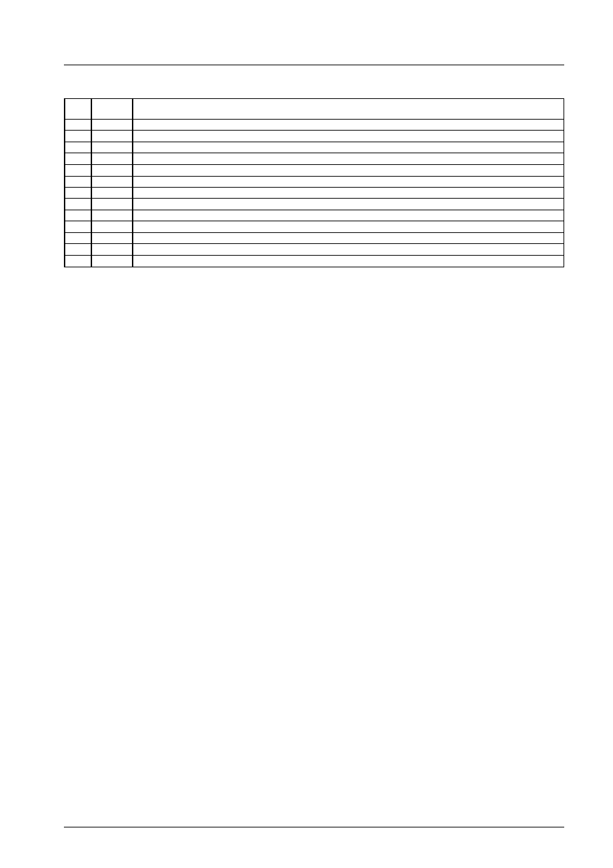
Continued from preceding page.
Pin
No.
Symbol
Contents
52
DAT
Microprocessor command data input pin.
53
CE
Microprocessor command chip enable input pin.
54
DRF
RF level detection output (Detect RF).
55
FSS
Focus search select; focus search mode (
�
search/+search vs. the reference voltage) switching pin
56
V
CC
2
Servo system and digital system V
CC
pin.
57
REFI
By-pass capacitor connection pin for reference voltage.
58
VR
Reference voltage output pin.
59
LF2
Disc defect detection time constant setting pin.
60
PH1
RF signal peak hold capacitor connection pin.
61
BH1
RF signal bottom hold capacitor connection pin.
62
LDD
APC circuit output pin.
63
LDS
APC circuit input pin.
64
V
CC
1
RF system V
CC
pin.
LA9240M
No.5482 - 5/20

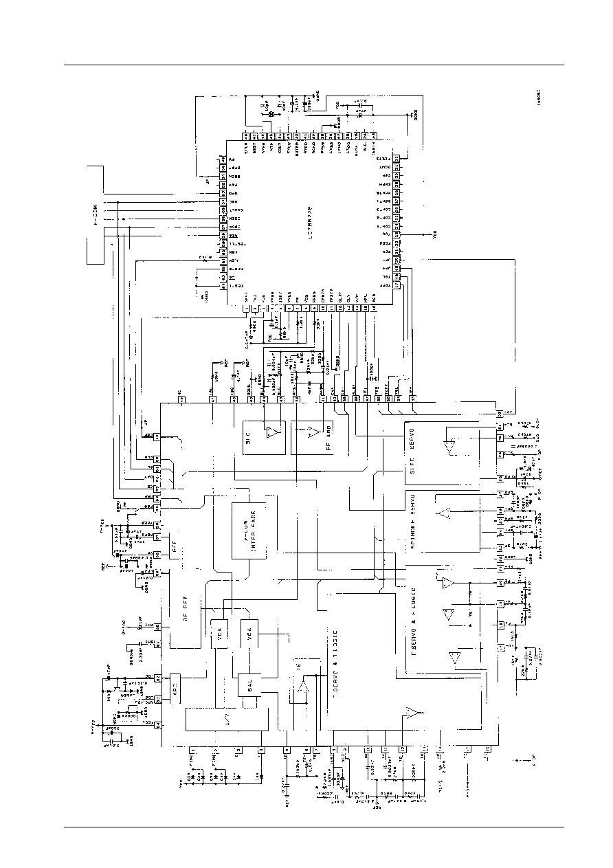
Equivalent Circuit Block Diagram
LA9240M
No.5482 - 6/20
Test Circuit
LA9240M
LA9240M
No.5482 - 7/20

Description of Operation
1.
APC (auto laser power control)
This circuit controls the pickup laser power. The laser is turned on and off by commands from the microprocessor.
2.
RF amplifier (eye pattern output)
The pickup photodiode output current (A + C) is input to FIN2 (pin 1), and (B + D) is input to FIN1 (pin 2). The current that
is input is converted to the voltage, passes through the AGC circuit, and is then output from the RFSM amplifier output
RFSM (pin 41). The internal AGC circuit has a variable range of �3 dB, and the time constant can be changed through the
external capacitor connected to PH1 (pin 60). In addition, this circuit also controls the bottom level of the EFM signal
(RFSM output), and the response can be changed through the external capacitor connected to BH1 (pin 61). The center gain
setting for the AGC variable range is set by the resistance between RFSM (pin 41) and RFS
-
(pin 42); if necessary, this
resistance is also used for 3T compensation for the EFM signal.
3.
SLC (slice level control)
The SLC sets the duty ratio for the EFM signal that is input to the DSP to 50%. The DC level is determined by integrating
the EFMO signal output from the DSP to determine the duty factor.
4.
Focus servo
The focus error signal is derived by detecting the difference between (A + C) and (B + D), which is (B + D) - (A + C), and
is then output from FE (pin 20). The focus error signal gain is set by the resistance between FE (pin 20) and FE
-
(pin 21).
Offset cancellation is performed by the FE amplifier. ``Offset cancellation'' cancels the offset for the IC's internal IV
amplifier, etc. Adjustment is initiated by the FOCUS-OFFSET ADJUST START command, and terminates after about 30 ms.
The FOCUS-OFFSET ADJUST OFF command is used to return to the state before offset cancellation.
The FA amplifier is the pickup phase compensation amplifier, and the equalizer curve is set by the external capacitor and
resistance. Furthermore, this amplifier has a mute function which is applied when V
CC
is turned on, when the F-SERVO OFF
command is sent, and during F-SEARCH. In order to turn the focus servo on, send either the LASER ON command or the
F-SERVO ON command.
The FD amplifier has a phase compensation circuit, and a focus search signal composition function and is completed in about
560 ms. Focus search is initiated by the F-SEARCH command, and a ramp waveform is generated by the internal clock. This
waveform is used for focus detection (focus zero cross) with the focus error signal and then turn the focus servo on. The
ramp waveform amplitude is set by the resistance between FD (pin 16) and FD
-
(pin 17).
FSC (pin 46) is for smoothing the focus search ramp waveforms, and a capacitor is connected between FSC and REF. FSS
(pin 55) is the focus search mode switching pin. If FSS is shorted with V
CC
, the ``+ search'' is set; if FSS is left open or is
shorted with GND, the ``
�
search'' is set.
5.
Tracking servo
The pickup photodiode output current is input to E (pin 3) and F (pin 4). The current that is input is converted to the voltage,
passes through the balance adjustment VCA circuit and then the VCA circuit that follows the gain in the RFAGC circuit, and
is then output from TE (pin 7). The tracking error gain is set by the resistance between TE
-
(pin6) and TE (pin7).
Offset cancellation is performed by the TE amplifier. Offset cancellation terminates after about 30 ms. The TRACK-OFFSET
ADJUST OFF command is used to return to the state before the offset.
The TH amplifier alters the servo response characteristics according to the THLD signal, etc., generated internally after
detection of the TGL signal from the DSP or the JP signal. When a defect is detected, the THLD mode goes into effect
internally. To avoid this, short DEF (pin 49) to L = GND. By inserting an external bandpass filter to remove the shock
component from the tracking error signal at SCI (pin 9), the gain is automatically boosted when a defect is detected.
The TA output (pin 11) has a built-in resistance to allow configuration of a low-pass filter.
The TD amplifier performs servo loop phase compensation; the characteristics are set by external CR. Furthermore, this
amplifier has a mute function, which is applied when V
CC
is turned on or the TRACK-SERVO OFF command is issued. The
muting function is released by the TRACK-SERVO ON command.
The TOFF amplifier that is positioned immediately after TD (pin 13) functions to turn off the servo in response to the TOFF
signal from the DSP.
The TO amplifier has a JP pulse composition function. The JP pulse is set by JP (pin 14). (THLD detection is performed
internally.)
6.
Sled servo
The response characteristics are set by SLEQ (pin 28). The amplifier positioned after SLEQ (pin 28) has a mute function that
is applied either when SLOF (pin 38) goes high or the SLED OFF command is issued. The sled is moved by inputting
current to SL
-
(pin 30) and SL
+
(pin 31); specifically, the pins are connected to the microprocessor output ports via resistors,
and the movement gain is set by the resistance value of that resistor. It is important to note that if there is a deviation in the
resistance values for SL
-
(pin 30) and SL
+
(pin 31), an offset will arise in the SLD output.
7.
Spindle servo
This configures the servo circuit, which maintains the linear velocity of the disc at a constant speed, along with the DSP. This
circuit accepts signals from the DSP through CV
-
(pin 39) and CV
+
(pin 40) and sets the equalizer characteristics through SP
(pin 23), SP
-
(pin 26), and SPD (pin 27), which are output to SPD (pin 27). The 12-cm mode amplifier gain is set by the
resistor connected between SPG (pin 25) and the reference voltage. In 8-cm mode, this amplifier serves as an internal buffer,
and SPG (pin 25) is ignored. Note that the gain setting is made for 8-cm mode first, and then 12-cm mode. If SPG (pin 25)
is left open, the gain is forcibly set for 8-cm mode, regardless of whether 8-cm or 12-cm mode is in effect.
LA9240M
No.5482 - 8/20
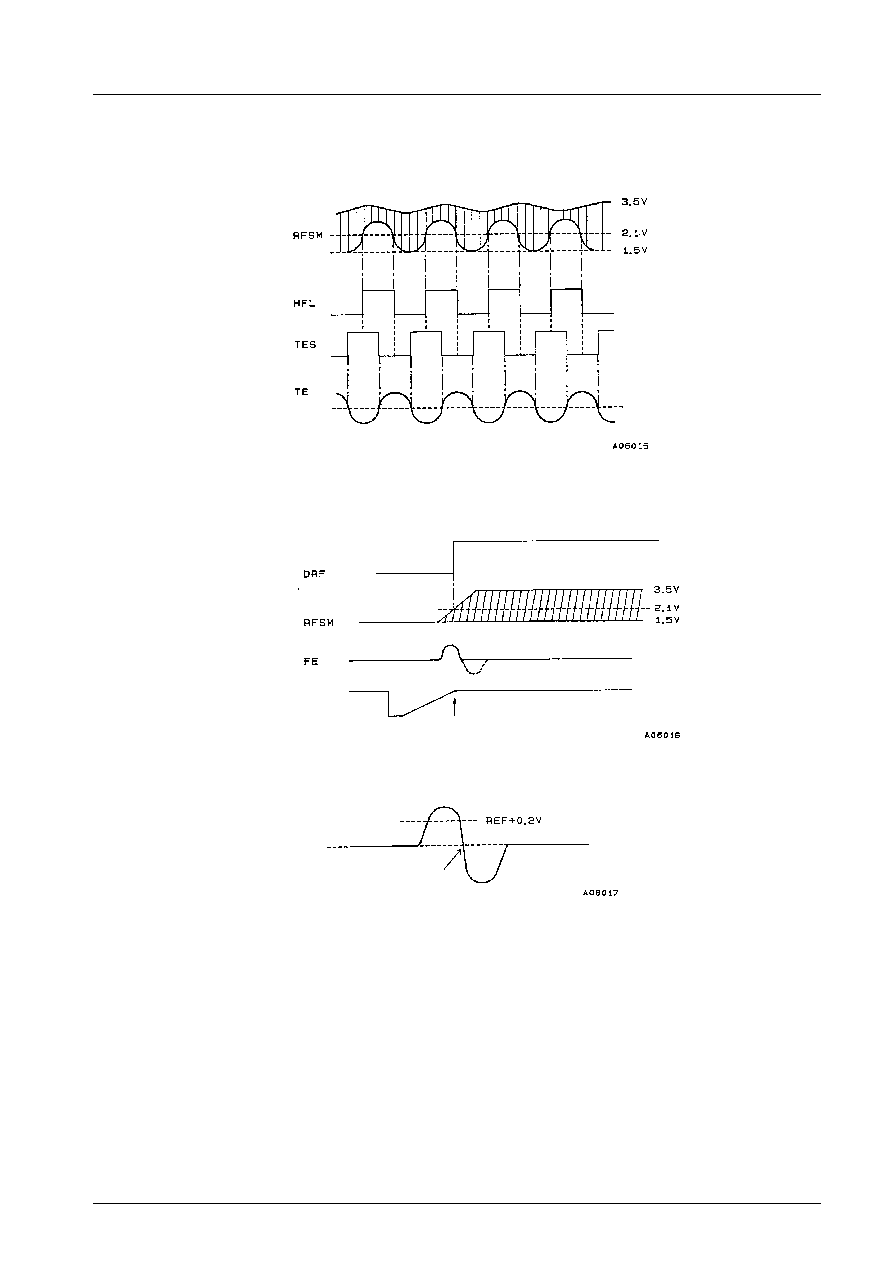
8.
TES and HFL (traverse signals)
When moving the pickup from the outer track to the inner track, the EF output from the pickup must be connected so that the
phase relationship of TES and HFL is as shown in the diagram below. For the TESI input, the TES comparator has negative
polarity and hysteresis of approximately �100 mV. An external bandpass filter is needed in order to extract only the required
signal from the TE signal.
9.
DRF (luminous energy determination)
DRF goes high when the peak of the EFM signal (RFSM output) held by the PH1 (pin 60) capacitor exceeds approximately
2.1 V. The PH1 (pin 60) capacitor affects the DRF detection time constant and the RFAGC response bidirectional setting. The
DRF output is driven by a constant current (250 �A).
Pickup position
Focus
10. Focus determination
Focus is assumed to be obtained when the focus error signal S curve reaching REF + 0.2 V is detected, and the S curve
subsequently returns to REF.
Focus
LA9240M
No.5482 - 9/20
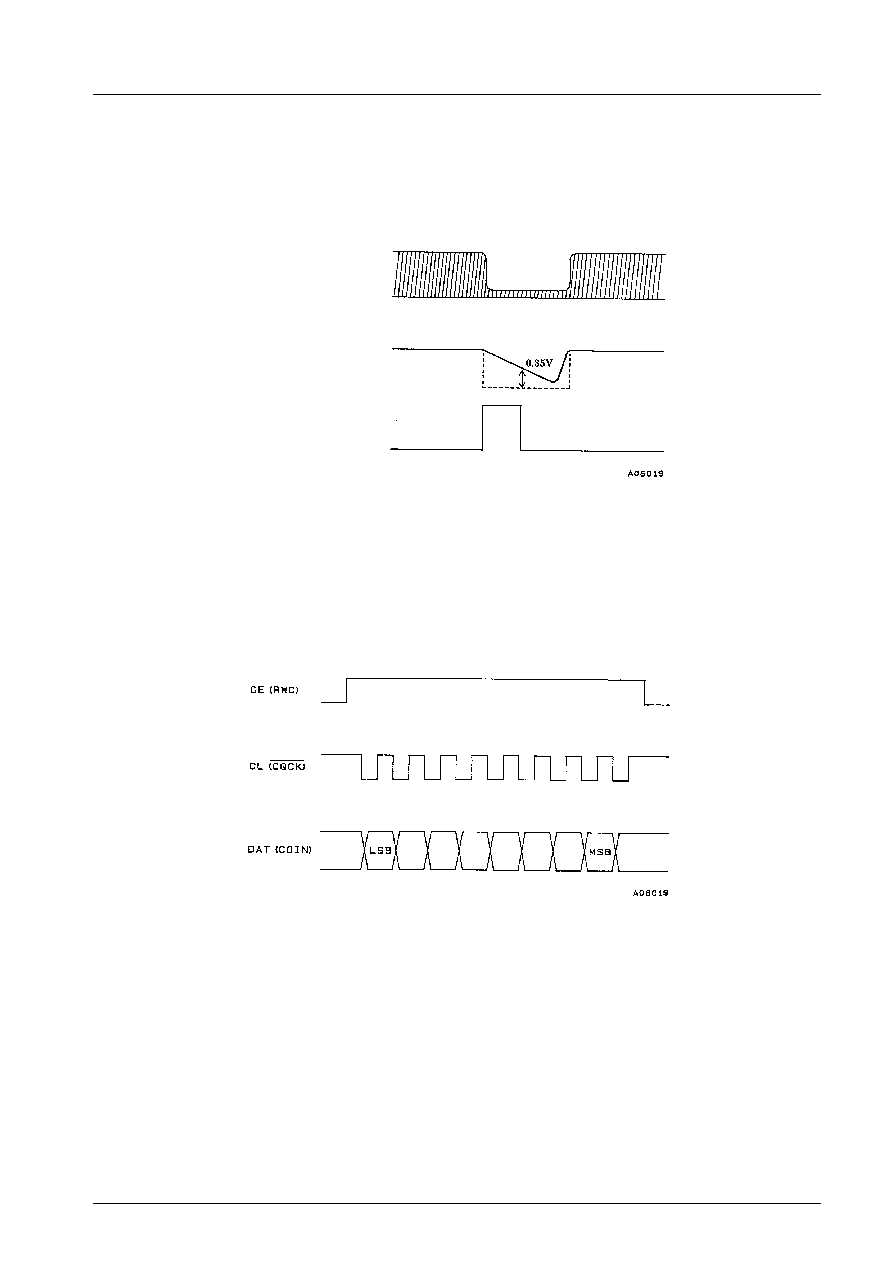
11. DEFECT
The mirrored surface level is maintained by the capacitor for LF2 (pin 59); when a drop in the EFM signal (RFSM output)
reaches 0.35 V or more, a high signal is output to DEF (pin 49). If DEF (pin 49) goes high, the tracking servo enters THLD
mode. In order to prevent the tracking servo from entering THLD mode when a defect is detected, prevent DEFECT from
being output by either shorting DEF (pin 49) to GND, or shorting LF2 (pin 59) to GND. The DEFECT output is driven by
constant current (approximately 100 �A).
12. Microprocessor interface
Because the Reset (Nothing) command initializes the LA9240M, it must be used carefully.
The LA9240M command acceptance (mode switching) timing is defined by the internal clock (4.23 MHz divided to 130 kHz)
after the falling edge of CE (RWC); therefore, when commands are sent consecutively, CE must go low for at least 10 �sec.
The 4.23 MHz clock is required for that reason. 2BYTE-COMMAND DETECT and 2BYTE-COMMAND RESET are used
only for the purpose of masking two-byte data.
All instructions can be input by setting CE high and sending commands synchronized with the CL clock from the
microprocessor to DAT (pin 52) in LSB first format. Note that the command is executed at the falling edge of CE.
13. Reset circuit
The power-on reset is released when V
CC
exceeds approximately 2.8 V.
14. Pattern design notes
To prevent signal jump-in from CV
+
(pin 40) to RFSM (pin 41), a shielding line is necessary in between.
15. V
CC
/REF/GND/NC
V
CC
1 (pin 64)
: RF system
V
CC
2 (pin 56)
: SERVO system, DIGITAL system
AGND (pin 22)
: RF system, SERVO system
DGND (pin 45)
: DIGITAL system
NC (pin 48)
: No connection
VR (Pin 58)
: Reference voltage
EFM signal
(RFSM output)
LF2 (pin 59)
DEF (pin 49)
Timing
* The DSP pin names are shown in parentheses.
LA9240M
No.5482 - 10/20
Microprocessor Command List
MSB
LSB
COMMAND
Reset mode
Power-on mode
DSP
0 0 0 0 0 0 0 0
RESET
RESET(NOTHING)
0 0 0 0 1 0 0 0
FOCUS START
FOCUS START #1
1 1 1 1 0 0 0 0
1 1 1 1 1 0 0 0
1 1 1 1 1 1 1 1
2BYTE-COMMAND DETECT
2BYTE-COMMAND DETECT
2BYTE-COMMAND RESET
2BYTE-COMMAND DETECT
2BYTE-COMMAND DETECT
2BYTE-COMMAND RESET
1 0 0 1 0 0 0 0
FOCUS-OFFSET ADJUST START
--
1 0 0 1 0 0 0 1
FOCUS-OFFSET ADJUST OFF
V
--
1 0 0 1 0 0 1 0
TRACK-OFFSET ADJUST START
--
1 0 0 1 0 0 1 1
TRACK-OFFSET ADJUST OFF
V
--
1 0 0 1 0 1 0 0
1 0 0 1 0 1 0 1
LASER ON
LASER OFF : F-SERVO ON
--
--
1 0 0 1 0 1 1 0
LASER OFF : F-SERVO OFF
V
--
1 0 0 1 0 1 1 1
SPINDLE 8CM
--
1 0 0 1 1 0 0 0
SPINDLE 12 CM
V
--
1 0 0 1 1 0 0 1
SPINDLE OFF
--
1 0 0 1 1 0 1 0
SLED ON
V
--
1 0 0 1 1 0 1 1
SLED OFF
--
1 0 0 1 1 1 0 0
E/F BALANCE START
Non-adjusted
--
1 0 0 1 1 1 0 1
TRACK-SERVO OFF
V
--
1 0 0 1 1 1 1 0
TRACK-SERVO ON
--
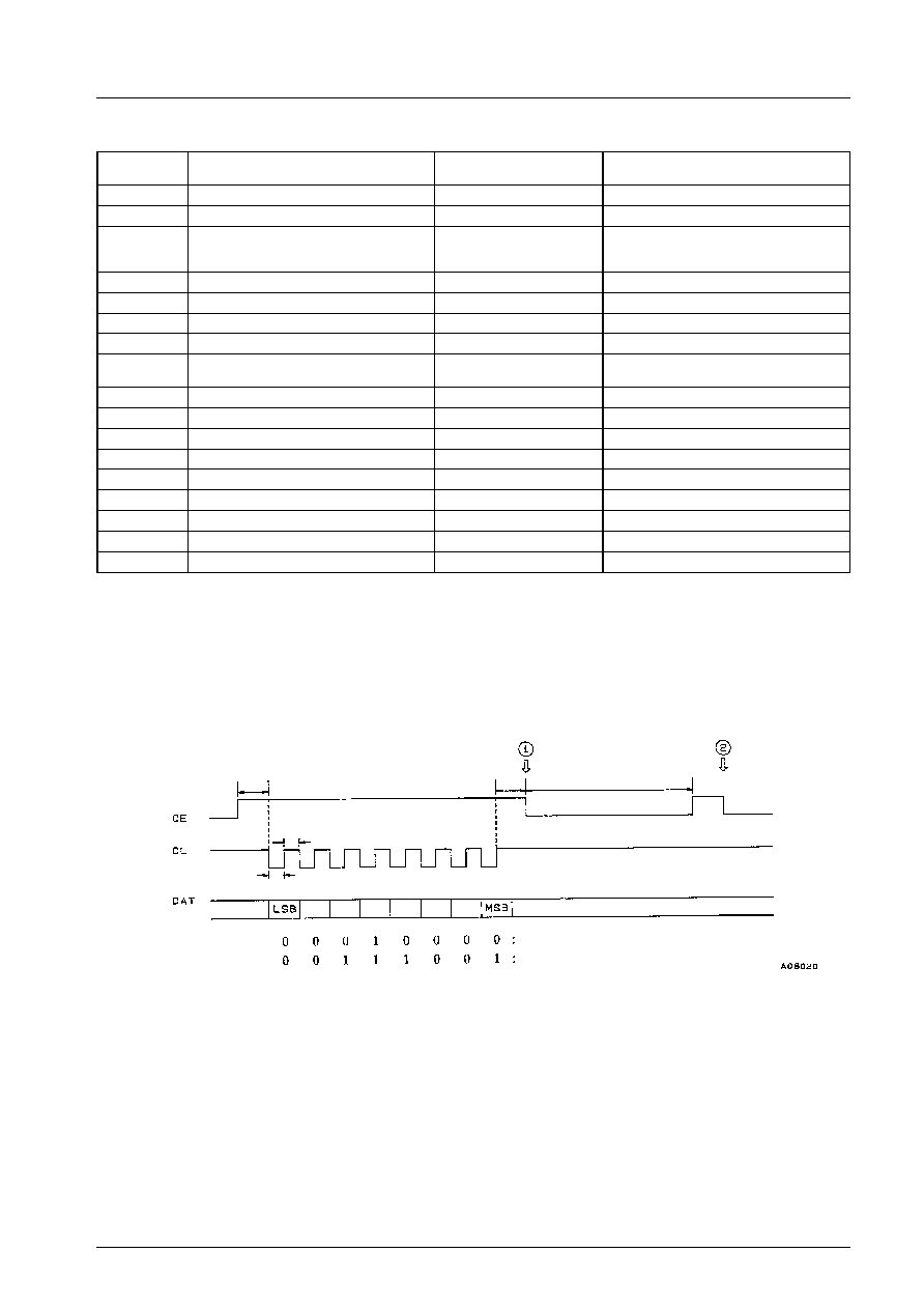
Notes Concerning Microprocessor Program Creation
1.
Commands
After sending the FOCUS START command and the E/F BALANCE START command, send 11111110 (FEH) in order to
clear the internal registers of the IC.
Reason: Although the above commands are executed at point 1 in the timing chart below, the same commands will be
executed again at point 2 if there is subsequent input to CE as shown below.
When sending a TRACK-OFFSET ADJUST START command or a FOCUS-OFFSET ADJUST START command after either
V
CC
ON (POWER ON RESET), RESET command, or a corresponding OFFSET ADJUST OFF command, waiting time is
necessary as listed below. (Only when a 4.2 MHz clock is input.)
TRACK-OFFSET ADJUST START: 4 ms or more
FOCUS-OFFSET ADJUST START: 4 ms or more
2.
E/F balance adjustment
E/F balance adjustments should be made in a bit region of the disc, not a mirrored region.
Since there is no track-kick for LA9240M, measures must be taken during EF balance adjustment to obtain a stable TE
signal. (By a sled movement signal from a microprocessor, for example.)
Timing
2 �s or more
1 �s or more
10 �s or more
1 �s or more
2 �s or more
``FOCUS START'' command
``E/F BALANCE START'' command
LA9240M
No.5482 - 11/20
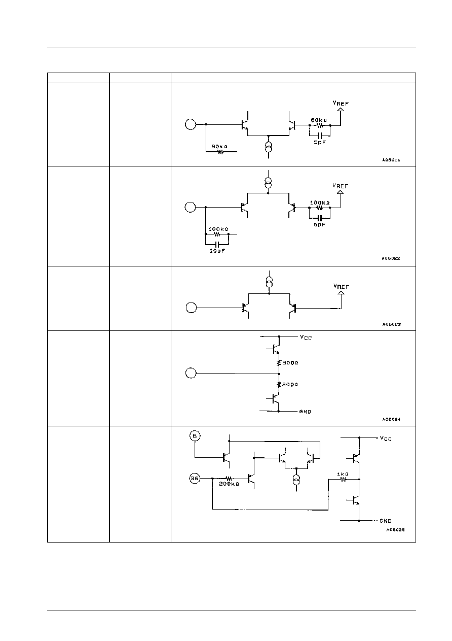
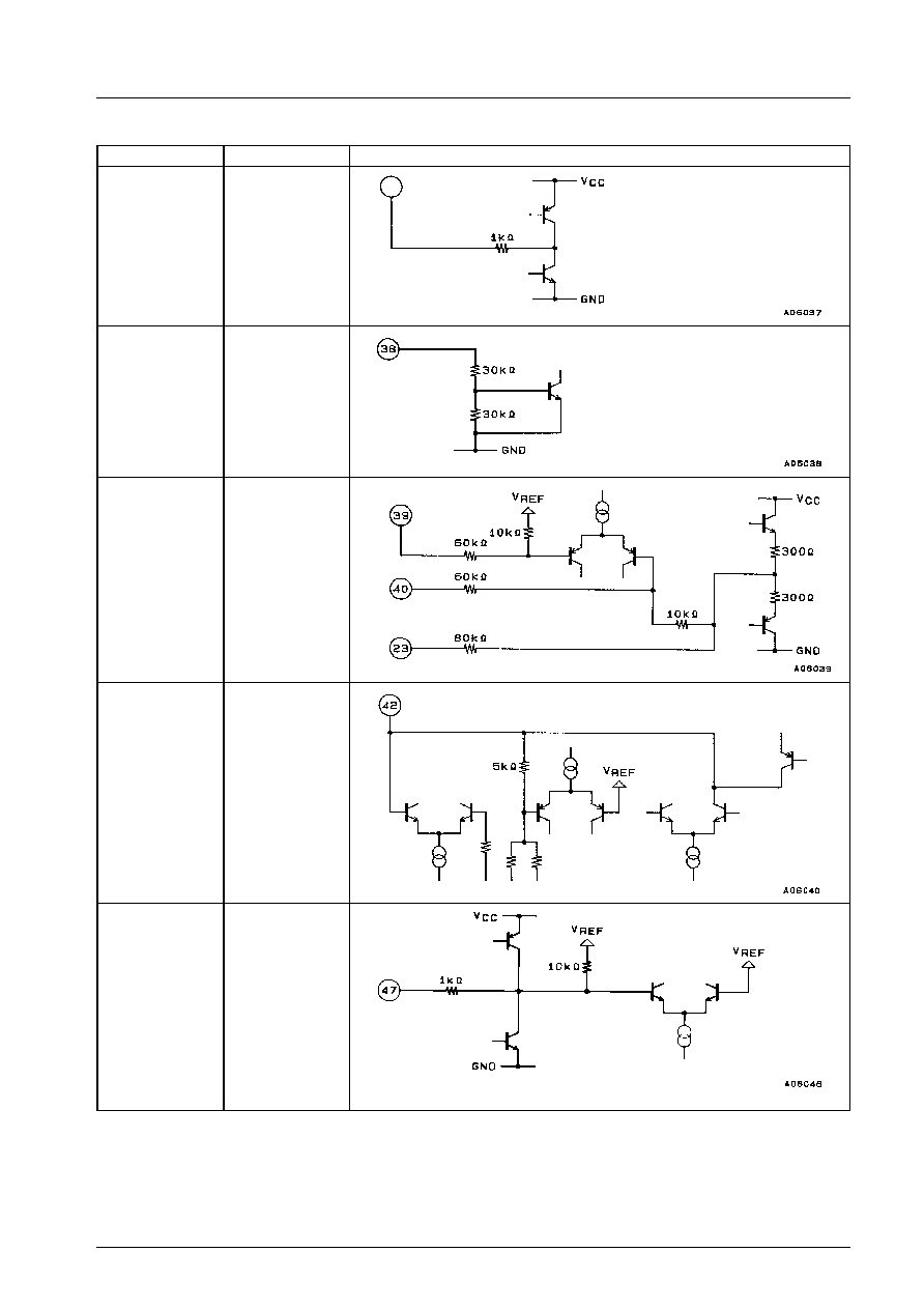
Pin Internal Equivalent Circuit
Pin No.
Pin Name
Internal Equivalent Circuit
1
2
FIN2
FIN1
3
4
E
F
5
6
17
21
26
28
44
TB
TE
�
FD
-
FE
-
SP
-
SLEQ
SLI
16
27
43
FD
SPD
SLC
8
36
TESI
TES
Continued on next page.
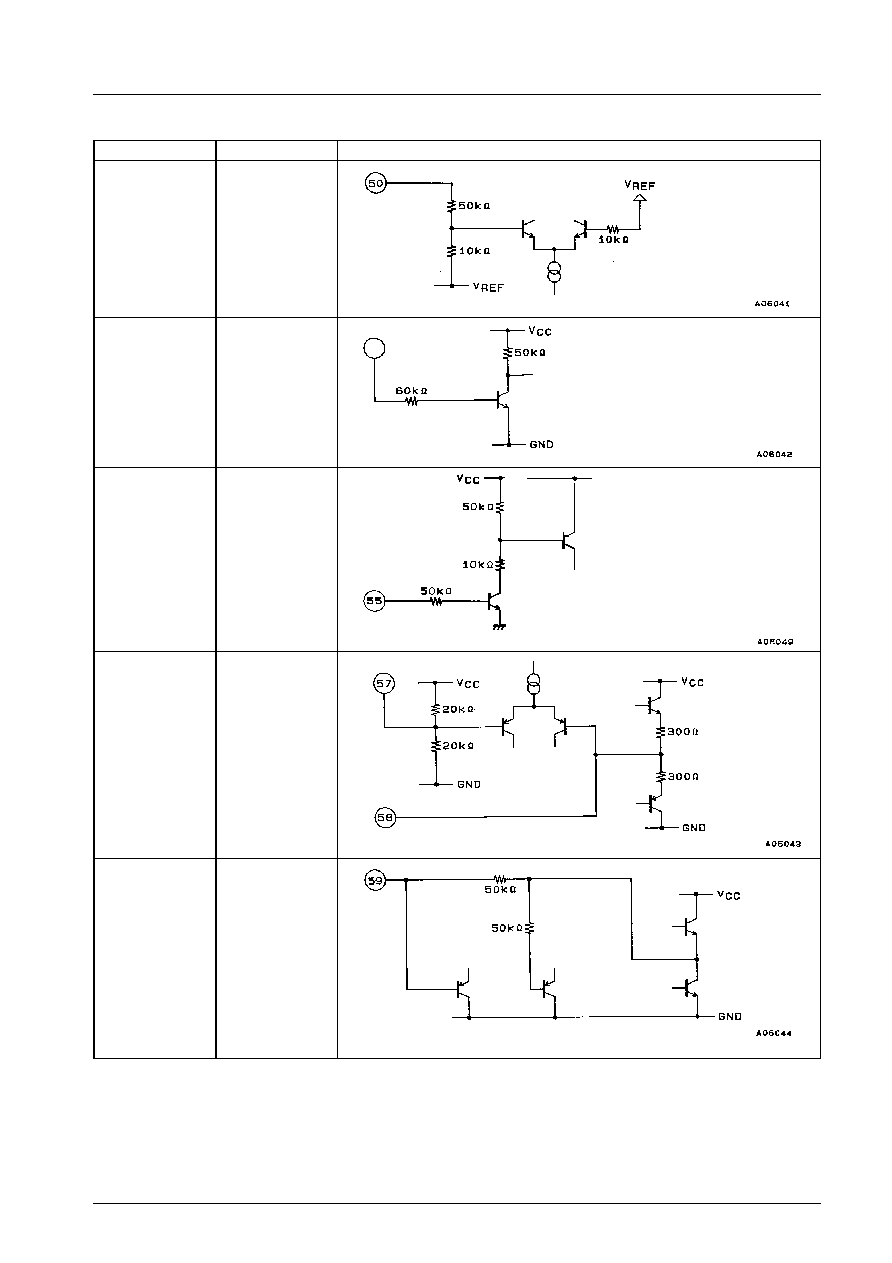
LA9240M
No.5482 - 12/20
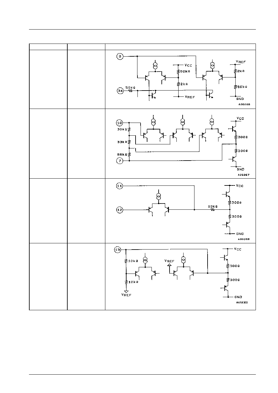
Continued from preceding page.
Pin No.
Pin Name
Internal Equivalent Circuit
9
34
SCI
TGL
7
10
TE
TH
11
12
TA
TD
-
13
TD
Continued on next page.
LA9240M
No.5482 - 13/20
Continued from preceding page.
Pin No.
Pin Name
Internal Equivalent Circuit
14
JP
15
TO
18
19
20
FA
FA
-
FE
Continued on next page.
LA9240M
No.5482 - 14/20
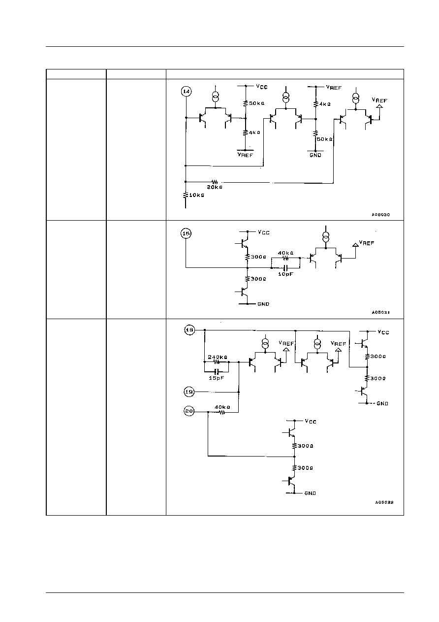
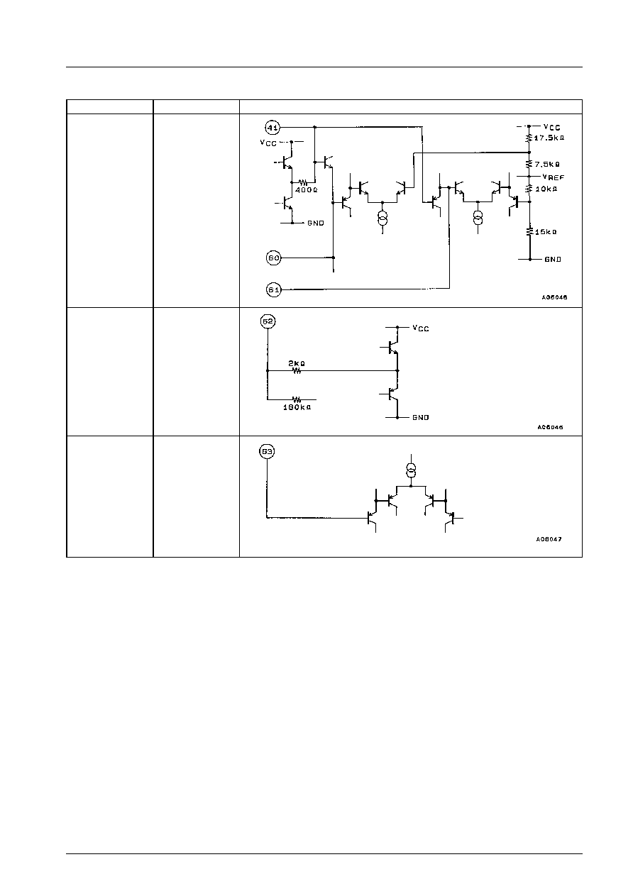
Continued from preceding page.
Pin No.
Pin Name
Internal Equivalent Circuit
24
25
SPI
SPG
29
30
31
SLD
SL
-
SL
+
32
33
JP
-
JP
+
35
TOFF
Continued on next page.
LA9240M
No.5482 - 15/20
Continued from preceding page.
Pin No.
Pin Name
Internal Equivalent Circuit
37
46
49
54
HFL
FSC
DEF
DRF
38
SLOF
39
40
23
CV
-
CV
+
SP
42
RFS
-
47
TBC
Continued on next page.
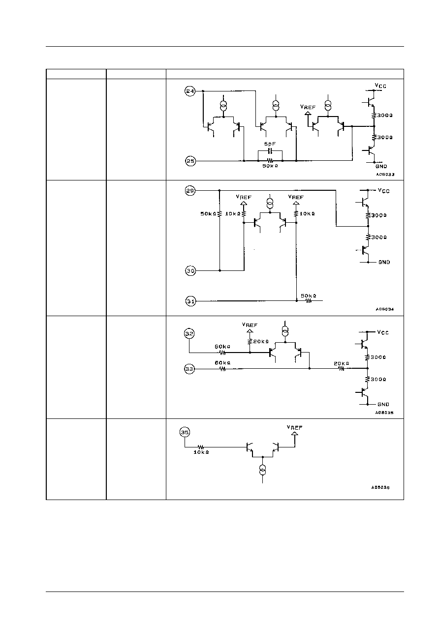
LA9240M
No.5482 - 16/20
Continued from preceding page.
Pin No.
Pin Name
Internal Equivalent Circuit
50
CLK
51
52
53
CL
DAT
CE
55
FSS
57
58
REFI
VR
59
LF2
Continued on next page.
LA9240M
No.5482 - 17/20
Continued from preceding page.
Pin No.
Pin Name
Internal Equivalent Circuit
41
60
61
RFSM
PH1
BH1
62
LDD
63
LDS
LA9240M
No.5482 - 18/20
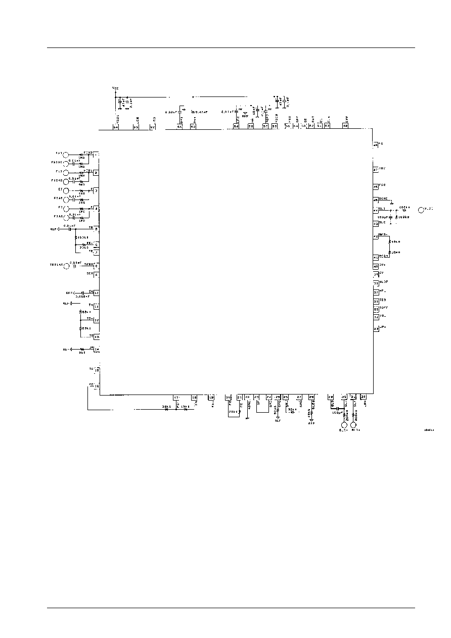
Sample Application Circuit
LA9240M
No.5482 - 19/20

No products described or contained herein are intended for use in surgical implants, life-support systems, aerospace equipment,
nuclear power control systems, vehicles, disaster/crime-prevention equipment and the like, the failure of which may directly or
indirectly cause injury, death or property loss.
Anyone purchasing any products described or contained herein for an above-mentioned use shall:
1
Accept full responsibility and indemnify and defend SANYO ELECTRIC CO., LTD., its affiliates, subsidiaries and distributors
and all their officers and employees, jointly and severally, against any and all claims and litigation and all damages, cost and
expenses associated with such use:
2
Not impose any responsibility for any fault or negligence which may be cited in any such claim or litigation on SANYO
ELECTRIC CO., LTD., its affiliates, subsidiaries and distributors or any of their officers and employees jointly or severally.
Information (including circuit diagrams and circuit parameters) herein is for example only; it is not guaranteed for volume
production. SANYO believes information herein is accurate and reliable, but no guarantees are made or implied regarding its use
or any infringements of intellectual property rights or other rights of third parties.
This catalog provides information as of August, 1997. Specifications and information herein are subject to change without notice.
LA9240M
No.5482 - 20/20