 | –≠–ª–µ–∫—Ç—Ä–æ–Ω–Ω—ã–π –∫–æ–º–ø–æ–Ω–µ–Ω—Ç: LA9250M | –°–∫–∞—á–∞—Ç—å:  PDF PDF  ZIP ZIP |

Ordering number : ENN5981
42800RM (OT) No. 5981-1/17
Overview
The LA9250M is a servo signal-processing IC for CD
players. In combination with a CD DSP such as the
LC78626KE, it can implement a CD player with a
minimal number of external components.
Functions
∑ I/V amplifier
∑ SLC
∑ FE
∑ Focus servo amplifier
∑ Spindle servo amplifier (with gain switching function)
∑ Focus detection (DRF and FZD)
∑ Defect detection
∑ RF amplifier with AGC
∑ APC
∑ TE (with variable gain and auto balance function)
∑ Tracking servo amplifier
∑ Sled servo amplifier (with turn-off function)
∑ Track detection (HFL, TES)
∑ Shock detection
Features
∑ Low-voltage operation: 2.4 V (minimum)
∑ Low current drain: 15 mA (at V
CC
= 3.0 V, typical)
∑ Built-in EF balance adjustment
∑ Built-in RF level AGC function
∑ RF level follower function for the tracking servo gain
(with turn-off function)
Package Dimensions
unit: mm
3159-QIP64E
14.0
17.2
1.0
1.0
1.6
0.15
0.35
0.1
15.6
0.8
0.8
3.0max
1
16
17
32
33
48
49
64
2.7
14.0
17.2
1.0
1.0
1.6
0.8
SANYO: QIP64E
[LA9250M]
LA9250M
SANYO Electric Co.,Ltd. Semiconductor Company
TOKYO OFFICE Tokyo Bldg., 1-10, 1 Chome, Ueno, Taito-ku, TOKYO, 110-8534 JAPAN
CD Player Analog Signal Processor (ASP)
Monolithic Linear IC
Any and all SANYO products described or contained herein do not have specifications that can handle
applications that require extremely high levels of reliability, such as life-support systems, aircraft's
control systems, or other applications whose failure can be reasonably expected to result in serious
physical and/or material damage. Consult with your SANYO representative nearest you before using
any SANYO products described or contained herein in such applications.
SANYO assumes no responsibility for equipment failures that result from using products at values that
exceed, even momentarily, rated values (such as maximum ratings, operating condition ranges, or other
parameters) listed in products specifications of any and all SANYO products described or contained
herein.
Parameter
Symbol
Conditions
Ratings
Unit
Maximum supply voltage
V
CC
max
Pin 56
7
V
Allowable power dissipation
Pd max
Ta
75∞C
200
mW
Operating temperature
Topr
≠15 to +75
∞C
Storage temperature
Tstg
≠40 to +150
∞C
Specifications
Maximum Ratings
at Ta = 25∞C, with pin 46 tied to ground

No. 5981-2/17
LA9250M
Parameter
Symbol
Conditions
Ratings
Unit
Recommended supply voltage
V
CC
3
V
Allowable operating supply voltage range
V
CC
op
2.4 to 5.5
V
Operating Conditions
at Ta = 25∞C, with pin 46 tied to ground
Parameter
Symbol
Conditions
Ratings
Unit
min
typ
max
Current drain
I
CCO
No input
8
14
21
mA
Reference voltage
V
REF
VR
1.2
1.5
1.8
V
[Interface]
SLOFvth
SLOFvth
SLOF
0.8
V
SP8vth
SP8vth
SP8: 8 cm mode
0.8
V
EFBALvth
EFBALvth EFBAL
2.3
V
FSTAvth
FSTAvth
ESTA
2.3
V
LASERvth
LASERvth LASER
0.8
V
CLK
CLK
R = 390 k
, C = 0.1 µF
25
35
45
Hz
[RF Amplifier]
RF no-signal voltage
RFo
0.75
1.00
1.25
V
Minimum gain
RF
G
min
FIN1, FIN2: 1 M
-input, PH1 = 2 V, f = 200 kHz, RF
≠15
dB
[Focus Amplifier]
FDO gain
FD
G
FIN1, FIN2: 1 M
-input, FDO
3.5
5.0
6.5
dB
FDO offset
FDost
The difference from the reference voltage, servo on.
≠340
0
+340
mV
F search voltage (high) 1
FS max1
FDO, FSS = GND
0.8
V
F search voltage (low) 1
FS min1
FDO, FSS = GND
≠0.8
V
F search voltage (high) 2
FS max2
FDO, FSS = V
CC
0.8
V
F search voltage (low) 2
FS min2
FDO, FSS = V
CC
0
V
[Tracking Amplifier]
TE gain max
TE
G
max
f = 10 kHz, E: 1 M
-input, PH1 = 0.5 V, TGRF = open
6.0
7.5
9.0
dB
TE gain min
TE
G
min
f = 10 kHz, E: 1 M
-input, PH1 = 2 V, TGRF = open
≠0.5
+1.8
+4.0
dB
TE-3dB
TEfc
E: 1 M
-input
70
kHz
TO gain
TO
G
TH
TO gain, THLD mode
10.0
12.0
14.0
dB
TGL offset
TGLost
Servo on, TGL = high, TO
≠260
0
+260
mV
TGH offset
TGHost
TGL = low, the difference from the TGL offset, TO
≠35
0
+35
mV
THLD offset
THDost
THLD mode, the difference from the TGL offset, TO
≠35
0
+35
mV
Off 1 offset
OFF1ost
TOFF = High
≠25
0
+25
mV
Balance range (high)
BAL-H
GainE/F input, TB = 3 V, TBC = open
+35
dB
Balance range (low)
BAL-L
GainE/F input, TB = 0 V, TBC = open
≠35
dB
TGLvth
TGLvth
0.8
1.5
1.8
V
PH no-signal voltage
PHo
The difference from RFSM
≠0.90
≠0.65
≠0.40
V
BH no-signal voltage
BHo10
The difference from RFSM
0.40
0.65
0.90
V
DRF detection voltage
DRFvth
At RFSM, the difference from VR
≠0.50
≠0.25
≠0.10
V
DRF output voltage (high)
DRF-H
2.5
2.9
V
DRF output voltage (low)
DRF-L
0
0.5
V
FZD detection voltage 1
FZD1
FE, the difference from VR
0
0.2
V
FZD detection voltage 2
FZD2
FE, the difference from VR
0
V
HFL detection voltage
HFLvth
At RF, the difference from VR
≠0.25
≠0.10
≠0.05
V
HFL output voltage (high)
HFL-H
2.5
2.9
V
HFL output voltage (low)
HFL-L
0
0.5
V
TES output voltage (low-high)
TES-LH
TESI, the difference from VR
≠0.15
≠0.10
≠0.05
V
TES output voltage (high-low)
TES-HL
TESI, the difference from VR
0.05
0.10
0.15
V
TES output voltage (high)
TES-H
2.5
2.9
V
TES output voltage (low)
TES-L
0
0.5
V
JP output voltage (high)
JP-H
TJP = 3 V, at TO, the difference from TJP = 1.5 V
0.05
0.25
0.45
V
Electrical Characteristics
at Ta = 25∞C, with pin 46 tied to ground, pin 56 = 3 V
Continued on next page.

No. 5981-3/17
LA9250M
Continued from preceding page.
Parameter
Symbol
Conditions
Ratings
Unit
min
typ
max
[Spindle Amplifier]
Offset 12
SPD12ost At SPD, the difference from VR, SP8 = 0 V: 12 cm mode
≠40
0
+40
mV
Offset 8
SPD8ost
At SPD, the difference from VR, SP8 = 3 V: 8 cm mode
≠40
0
+40
mV
Offset off
SPDof
At SPD, the difference from VR, SP8 = 3 V: 8 cm mode
≠40
0
+40
mV
Output voltage H12
SPD-H12
The difference from offset 12,
0.35
0.50
0.65
V
SP8 = 0 V, 12 cm mode, CLV = 3 V
Output voltage H8
SPD-H8
The difference from offset 8,
0.10
0.20
0.30
V
SP8 = 3 V, 8 cm mode, CLV = 3 V
[Sled Amplifier]
Offset SLD
SLDost
SLEQ = VR, the difference from VR
≠80
0
+80
mV
Offset off
SLDof
SLOF = High
≠40
0
+40
mV
SLC no-signal voltage
SLCo
SLC
1.0
1.5
2.0
V
Shock no-signal voltage
SCIo
SCI, the difference from VR
≠40
0
+40
mV
Shock detection voltage (high)
SCIvthH
SCI, the difference from VR
90
140
190
mV
Shock detection voltage (low)
SCIvthL
SCI, the difference from VR
≠190
≠140
≠90
mV
The difference between the LF2 voltage when DEF is
DEF detection voltage
DEFvth
detected with RF = 1.9 V and the LF2 voltage when
0.20
0.35
0.50
V
RF = 1.9 V.
DEF output voltage (high)
DEF-H
2.5
2.9
V
DEF output voltage (low)
DEF-L
0
0.5
V
APC reference voltage
LDS
The LDS voltage such that LDD = 1.5 V
120
170
220
mV
APC off voltage
LDDof
LDD
2.7
2.9
V
Pin Functions
Pin No.
Pin
Function
1
FIN2
Pickup photodiode (focus, RF) connection
2
FIN1
Pickup photodiode (focus, RF) connection
3
E
Pickup photodiode (tracking) connection
4
F
Pickup photodiode (tracking) connection
5
TB
TE signal DC component input. Pickup photodiode (tracking) connection
6
TE
≠
TE signal gain setting resistor connection. A resistor is connected between this pin and TE.
7
TE
TE signal output
8
TESI
TES comparator input. Takes the bandpass filtered TE signal as its input.
9
SCI
Shock detection input
10
TH
Tracking gain time constant setting
11
TA
TA amplifier output
12
TD
≠
In conjunction with the TD and VR pins, used to form the tracking phase compensation circuit constant
13
TD
Tracking phase compensation setting
14
JP
Track jump signal amplitude setting
15
TO
Tracking control signal output
16
(NC)
No connection
17
FD
Focusing control signal output
18
FD
≠
In conjunction with the FD and FA pins, used to form the focusing phase compensation circuit constant
19
FA
In conjunction with the FD- and FA- pins, used to form the focusing phase compensation circuit constant
20
FA
≠
In conjunction with the FA and FE pins, used to form the focusing phase compensation circuit constant
21
FE
FE signal output
22
FE
≠
FE signal gain setting resistor connection. A resistor is connected between this pin and FE.
23
SP
CLV pin input signal inverted output
24
SPG
Gain setting resistor connection (12 cm spindle mode)
Continued on next page.

No. 5981-4/17
LA9250M
Continued from preceding page.
Pin No.
Pin
Function
25
SP
≠
In conjunction with the SPD pin, spindle phase compensation time constant connection
26
SPD
Spindle control signal output
27
SLEQ
Sled phase compensation time constant connection
28
SLD
Sled control signal output
29
SL
≠
Sled feed signal input from the microcontroller
30
SL
+
Sled feed signal input from the microcontroller
31
OSC
Oscillator frequency setting
32
(NC)
No connection
33
SLOF
Sled servo off control input
34
TGRF
Tracking servo gain RF level follower function setting
35
SP8
Spindle 8 cm/12 cm mode switching control from the DSP
36
EFBAL
E/F balance adjustment signal input from the DSP
37
FSTA
Focus search control signal input from the DSP
38
LASER
Laser on/off control from the DSP
39
(NC)
No connection
40
TJP
Track jump signal input from the DSP
41
TGL
Tracking gain control signal input from the DSP
42
TOFF
Tracking off control signal input from the DSP
43
TES
TES signal output to the DSP
44
HFL
Output for the HFL signal that indicates whether the main beam is positioned over pits or mirror
45
CLV
CLV error signal input from the DSP
46
GND
GND
47
RF
RF output
48
RF
≠
In conjunction with the RF pin, sets the RF gain and sets the EFM 3T compensation
49
SLC
Output for control of the RF waveform data slice level according to the DSP
50
SLI
Input for control of the RF waveform data slice level according to the DSP
51
DEF
Disc defect detection output
52
DRF
RF level detection output
53
FSC
Focus search smoothing capacitor output
54
TBC
E/F balance variation range setting
55
FSS
Focus search mode setting
56
V
CC
V
CC
57
REFI
Reference voltage bypass capacitor connection
58
VR
Reference voltage output
59
LF2
Disc defect detection time constant setting
60
PH1
RF signal peak hold capacitor connection
61
BH1
RF signal bottom hold capacitor connection
62
LDD
APC circuit output
63
LDS
APC circuit input
64
(NC)
No connection

No. 5981-5/17
LA9250M
Pin Circuits
Pin No.
Pin
Internal equivalent circuit
1
2
FIN2
FIN1
1
62k
62k
5pF
VREF
2
3
4
E
F
3
100k
100k
5pF
5pF
VREF
4
5
6
18
22
25
27
50
TB
TE
≠
FD
≠
FE
≠
SP
≠
SLEQ
SLI
5
VREF
6
18
22
25
27
50
7
10
TE
TH
10
7
250
GND
VCC
30k
33k
68k
8
43
TESI
TES
8
43
1k
200k
GND
VCC
Continued on next page.

No. 5981-6/17
LA9250M
Continued from preceding page.
Pin No.
Pin
Internal equivalent circuit
9
41
SCI
TGL
41
9
4k
50k
GND
VREF
50k
50k
4k
VREF
VCC
11
12
TA
TD
≠
12
11
10k
GND
VCC
13
TD
13
250
GND
VCC
14
JP
14
4k
20k
50k
GND
VCC
50k
4k
10k
VREF
VCC
VREF
15
TO
15
250
40k
100k
10pF
GND
VCC
VREF
VREF
Continued on next page.

No. 5981-7/17
LA9250M
Continued from preceding page.
Pin No.
Pin
Internal equivalent circuit
17
26
49
FD
SPD
SLC
17
26
49
250
GND
VCC
19
20
21
FA
FA
≠
FE
19
20
21
250
240k
15pF
GND
VCC
250
GND
VCC
VREF
40k
VREF
23
45
SP
CLV
45
23
250
30k
10k
80k
10k
GND
VCC
VREF
24
SPG
VREF
50k
80k
5pF
24
23
SP
250
GND
VCC
Continued on next page.

No. 5981-8/17
LA9250M
Continued from preceding page.
Pin No.
Pin
Internal equivalent circuit
28
29
30
SLD
SL
≠
SL
+
28
29
30
250
40k
40k
50k
50k
GND
VCC
VREF
VREF
31
OSC
VCC
31
33
35
38
SLOF
SP8
LASER
33
30k
GND
34
TGRF
34
36
37
EFBAL
FSTA
30k
50k
20k
VCC
GND
36
40
TJP
40
250
30k
20k
20k
GND
VCC
VREF
Continued on next page.

No. 5981-9/17
LA9250M
Continued from preceding page.
Pin No.
Pin
Internal equivalent circuit
42
TOFF
30k
60k
VCC
GND
42
44
51
52
53
HFL
DEF
DRF
FSC
44
52
51
53
1k
GND
VCC
47
60
61
RF
PH1
BH1
47
60
61
28k
5k
10k
15k
250
VREF
VCC
VCC
GND
GND
48
RF
≠
48
3k
VREF
VREF
5k
5k
5k
54
TBC
54
VREF
10k
VREF
1k
GND
VCC
Continued on next page.

No. 5981-10/17
LA9250M
Continued from preceding page.
Pin No.
Pin
Internal equivalent circuit
55
FSS
55
VCC
GND
50k
50k
57
58
REFI
VR
57
58
VCC
GND
100
VCC
GND
20k
20k
59
LF2
59
VCC
GND
50k
1k
5k
62
LDD
62
200
VCC
GND
180k
63
LDS
63

Equivalent Circuit
No. 5981-11/17
LA9250M
APC
LA9250M
VCA
SLED SERVO
F. SERVO
&F. LOGIC
I/V
RF DET
REF
SLC
RF AMP
BAL
TE
T. SERVO
&T. LOGIC
SPINDLE
SERVO
LATCH
7
SLC
SLI
DEF
DRF
FSC
TBC
FSS
V
CC
REFI
VR
LF2
PH1
BH1
LDD
FD
FD
-
FA
FA
-
FE
FE
-
SP
SP
-
SPG
SPD
SLEQ
SLD
OSC
NC
SL
-
SL
+
NC
LDS
REF
T
OFF
NC
TO
JP
TD
TD
-
TA
TH
SCI
TESI
TE
TB
F
TE
-
E
FIN1
FIN2
VCA
A11345
17
18
19
20
21
22
23
24
25
26
27
28
29
30
31
32
64
1
2
3
4
5
6
7
8
9
10
11
12
13
14
15
16
62
61
60
59
57
56
55
54
53
52
51
50
49
48
47
46
45
44
43
42
41
40
39
38
37
36
35
34
33
58
63
SLOF
TGRF
SP8
EFBAL
FSTA
LASER
NC
TJP
TGL
TOFF
TES
HFL
CLV
GND
RF
RF
-

Operation
1. APC (Auto Laser Power Control)
This circuit controls the laser power, turning the laser on and off (pin 38). The laser is turned on when the LASER pin
is high.
2. RF amplifier (eye pattern output)
The pickup photodiode output current input to FIN1 (pin 2) and FIN2 (pin 1) is I/V converted, passed through an
AGC circuit, and output from the RFSUM amplifier RF pin (pin 47). The built-in AGC circuit has a variable range of
about ±4 dB, and its time constant is set by the external capacitor connected to PH1 (pin 60). The EFM signal bottom
level is also controlled, and the response is set by the external capacitor attached to PH1 (pin 60). The center gain for
the AGC variable range is set by the value of the resistor between RF (pin 47) and RF- (pin 48). If required, these
pins can also be used for EFM signal 3T compensation.
3. SLC (Slice Level Controller)
Since the SLC circuit sets the duty of the EFM signal input to the DSP to 50%, the DC level is controlled by
integrating the EFMO signal from the DSP.
4. Focus Servo
The focus error signal is acquired by detecting the difference between (A + C) and (B + D) from the pickup and the
result is output from FE (pin 21). The FE signal gain is set by the value of the resistor between FE and FE
≠
(pin 22).
The FA amplifier is the pickup phase compensation amplifier, and its equalization curve is set by an external
capacitor and resistor.
The FD amplifier provides a phase compensation circuit and a focus search signal synthesis function.
A focus search operation is started by switching FSTA (pin 37) from low to high. A ramp waveform is generated by
an internal oscillator; this ramp completes in about 560 ms. We recommend holding FSTA (pin 37) high until another
focus search is to be performed. Focus is detected (the focus zero cross state) from the focus error signal generated, in
effect, by this waveform, and this turns the focus servo on. The ramp waveform amplitude is set by the value of the
resistor between FD (pin 17) and FE
≠
(pin 18).
Since FSC (pin 53) is used to smooth the focus search ramp waveform, a capacitor is connected between FSC and VR
(pin 58). FSS (pin 55) switches the focus search mode; when FSS is shorted to V
CC
the circuit performs a + search
with respect to the reference voltage VR, and when open or shorted to ground, it performs a ± search.
5. Tracking Servo
The pickup photodiode output current input to E (pin 3) and F (pin 4) is I/V converted and passed first through a
balance adjustment VCA circuit and then through a VCA circuit that performs gain following for the RF AGC circuit.
The resulting signal is then output from TE (pin 7). The gain follower function can be turned off by setting TGRF
(pin 34) high.
The tracking error gain is set by the value of the resistor between TE
≠
(pin 6) and TE (pin 7).
The TH amplifier detects either the JP signal or the TGL signal from the DSP, and functions to change the response
characteristics of the servo according to the THLD signal generated internally. When a defect is detected, the circuit
switches to THLD mode internally. Set DEF (pin 51) low to prevent this. Note that an external bandpass filter that
extracts only the shock component from the tracking error signal is formed on SCI (pin 9), and that the gain is
automatically increased if this signal is inserted.
The TA output (pin 11) has an internal resistor so that a low-pass filter can be formed.
The TD amplifier circuit is provided to perform servo loop phase compensation, and its characteristics are set by
external RC components. This amplifier also provides a muting function, and the servo can be turned off by setting
TOFF (pin 42) high.
The TO amplifier provides a function for synthesizing JP pulses, and JP (pin 14) is used to set the JP pulse
conditions.
The E/F balance adjustment operation is started by switching EFBAL (pin 36) from low to high. After that, the
adjustment operation is performed by a clock generated by an internal oscillator, and the adjustment completes in
about 500 ms. We recommend holding EFBAL (pin 36) high until the next time an E/F balance operation is to be
performed.
No. 5981-12/17
LA9250M

This adjustment operation must be performed over the disc pit area, not over the disc mirror area. Note that
applications must take measures to assure that a stable TE signal is acquired so that track kick operations do not occur
during the adjustment. (This includes sled feed commands from the microcontroller.)
The E/F balance adjustment precision and adjustment range can be set to be optimal for the pickup characteristics by
the value of the resistor between TBC (pin 54) and the reference voltage, VR.
6. Sled Servo
The response characteristics are set at SLEQ (pin 27). The amplifier that follows SLEQ has a muting function, and
the sled servo can be turned off by setting SLOF (pin 33) high.
Sled feed is performed in a current input form at SL
≠
(pin 29) and SL
+
(pin 30). In particular, a resistor is connected
to a microcontroller output port and the feed gain is set by the value of that resistor.
7. Spindle Servo
A servo circuit that holds the disc at a constant linear velocity is formed by the internal servo circuit in conjunction
with the DSP. A signal from the DSP is accepted by CLV (pin 45), and output from SPD (pin 26). The phase
compensation characteristics are set by SP (pin 23), SP
≠
(pin 25), and SPD. The 12 cm mode amplifier gain is set by a
resistor connected between SPG (pin 24) and the reference voltage. In 8 cm mode, this amplifier is internally buffered
and not affected by SPG. The circuit switches to 8 cm mode when SP8 (pin 35) is set high.
8. TES and HFL (Traversal signal)
The sub-beam signals from the pickup are connected to E (pin 3) and F (pin 4) so that HFL and TES have the phase
relationship shown in the figure when the pickup moves from the outside towards the inside of the disc. The TES
comparator has a hysteresis of about ±100 mV at the minus polarity of the comparator with respect to the TESI (pin
8) input. An external bandpass filter is formed so that only the required signal is extracted from the TE signal.
9. DRF (Optical level decision)
A peak hold operation is applied to the EFM signal (RF output) by a capacitor at PH1 (pin 60), and DRF goes high
when the RF peak value exceeds about 1.3 V (when V
CC
= 3.0 V). The PH1 capacitor is related to the settings of both
the DRF detection time constant and the RF AGC response.
No. 5981-13/17
LA9250M
RFSM
HFL
TES
TE
2.0 V
1.4 V
1.0 V
A11267
DRF
RFSM
FE
Pickup position
Focus
2.0 V
1.3 V
1.0 V
A11268

10. Focus Detection
The pickup is seen as being in focus when, after a VR + 0.2 V level is detected in the focus error signal S-curve, that
S-curve next goes to the VR level.
11. Defect Detection
The mirror surface level is held by the capacitor on LF2 (pin 59), and DEF (pin 51) goes high if a drop in the EFM
signal (RF output) exceeds about 0.35 V. When DEF goes high, the tracking servo goes to THLD mode. When a
defect is detected applications can prevent the LA9250M from going to THLD mode either by setting DEF to low or
by setting LF2 (pin 59) low and thus setting the LA9250M not to output DEF.
12. Oscillator Circuit
The oscillator frequency is set by the external RC circuit attached to OSC (pin 31). This oscillator frequency is used
as the reference clock for focus search and E/F balance adjustment.
No. 5981-14/17
LA9250M
Focus
REF + 0.2 V
A11269
EFM signal
(RFSM output)
LF2 (pin 59)
DEF (pin 51)
0.35 V
A11270
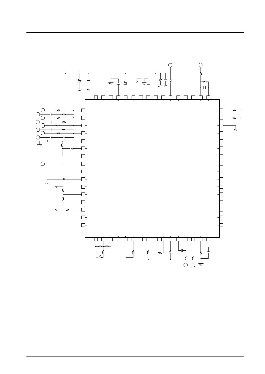
Test Circuit
No. 5981-15/17
LA9250M
47
µ
F
0.1
µ
F
SLC
SLI
DEF
DRF
FSC
TBC
TBC
FSS
V
CC
REFI
VR
LF2
PH1
BH1
LDD
FD
FD
-
FA
FA
-
FE
FE
-
SP
SP
-
SPG
SPD
SLEQ
REF
SLD
OSC
NC
SL
-
SL
+
68k
68k
24k
20k
50k
100k
NC
LDS
10k
SLI
-
SLI
+
0.068
µ
F
100pF
0.01
µ
F
0.01
µ
F
0.01
µ
F
REF
15k
200k
200k
390k
V
CC
REF
2k
15k
30k
39k
S1
20k
1M
1M
REF
REF
NC
TO
JP
TD
TD-
TA
TH
SCI
TESI
TESI AC
TE
TB
F
TE-
E
FIN1
FIN2
A11346
0.01
µ
F
1M
1M
0.01
µ
F
1M
1M
0.01
µ
F
1M
1M
F1I
EI
FI
F2I
F2IAC
F1IAC
EIAC
FIAC
0.33
µ
F
0.47
µ
F
47
µ
F
0.1
µ
F
0.1
µ
F
100k
0.1
µ
F
10k
2k
SLI1
100k
17
18
19
20
21
22
23
24
25
26
27
28
29
30
31
32
0.1
µ
F
64
61
60
59
57
56
55
54
53
52
51
50
49
47
48
46
45
44
43
42
41
40
39
38
37
36
35
34
33
2
1
3
4
5
6
7
8
9
10
11
12
13
14
15
16
58
63
62
SLOF
TGRF
SP8
EFBAL
FSTA
LASER
NC
TJP
TGL
TOFF
TES
HFL
CLV
GND
RF
RF-
73
72
71
70
69
68
67
66
65
77
76
75
74
LA9250M
No. 5981-16/17
LA9250M
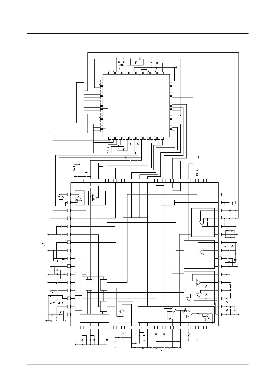
Sample Application Circuit
APC
LA9250M
VCA
SLED SERVO
F. SERVO
&F. LOGIC
I/V
RF DET
REF
SLC
RF AMP
BAL
TE
T. SERVO
&T. LOGIC
SPINDLE
SERVO
LATCH
V
DD
GND
GND
VDD
10pF
10pF
7
GND
GND
10k
10
µ
F
100
µ
F
0.33
µ
F
47
µ
F
0.1
µ
F
10
µ
F
0.047
µ
F
0.047
µ
F
0.15
µ
F
0.1
µ
F
REF
REF
0.01
µ
F
220
µ
F
47
µ
F
APC.ADJ
LASER
1
µ
F
100
µ
F
FSS.SW:Hi +F-SEARCH
LOW: +-
F-SEARCH
0.022
µ
F
0.01
µ
F
4.7
µ
F
SLC
SLI
DEF
DRF
FSC
TBC
FSS
VCC
REFI
VR
LF2
PH1
BH1
LDD
10k
15k
1.8k
470k
470k
24k
FD
FD-
FA
FA-
FE
FE-
SP
SP-
SPG
SPD
SLEQ
REF
REF
SLD
OSC
NC
SL-
SL
+
39k
0.0047
µ
F
47k
56k
P-CP
220k
2.2k
REF
4.7k
560
56k
220k
10k
100k
10
NC
LDS
20k
4pF
10k
51k
10pF
V
DD
0.001
µ
F
0.033
µ
F
330
56k
22k
15k
15k
9.1k
MCN1
0.01
µ
F
0.001
µ
F
0.0033
µ
F
0.47
µ
F
100pF
P-CP
P-CP
SLD
-
SLD
+
0.001
µ
F
0.22
µ
F
33k
0.15
µ
F
2.7k
0.01
µ
F
P-CP
330
µ
F
0.033
µ
F
0.22
µ
F
0.0033
µ
F
0.22
µ
F
47
µ
F
GND
GND
GND
GND
GND
GND
V
CC
REF
D-V
CC
REF
V
CC
V
CC
DXX
DXX
DXX
DXX
DXX
DXX
2.2k
REF
TOFF
REF
390k
0.1
µ
F
47
µ
F
0.01
µ
F
0.1
µ
F
330
22k
680
33k
56k
1.2k
0.1
µ
F
100
µ
F
0.1
µ
F
GND
NC
TO
JP
TD
TD
-
TA
TH
SCI
TESI
TE
TB
F
TE
-
E
FIN1
FIN2
VCA
TGRF.Hi TE GAIN DCES NOT FOLLOW RF LEVEL.
Micro-controller
A11271
V
CC
17
18
19
20
21
22
23
24
25
26
27
28
29
30
31
32
64
1
2
3
4
5
6
7
8
9
10
11
12
13
14
15
16
62
61
60
59
57
56
55
54
53
52
51
50
49
48
47
46
45
44
43
42
41
40
39
38
37
36
35
34
33
58
63
SLOF
TGRF
SP8
EF
BAL
FSTA
LASER
NC
TJP
TGL
TOFF
TES
HFL
CLV
GND
RF
RF
-
64
1
2
3
4
5
6
7
8
9
10
11
12
13
14
15
16
48
47
46
45
44
43
42
41
40
39
38
37
36
35
34
33
63
62
61
60
59
58
57
56
55
54
53
52
51
50
49
LC78626KE
DEF1
TAI
PDO
VV
SS
ISET
VV
DD
FR
V
SS
EFMO
EFMIN
TEST2
CLV+
CLV-
V/P
HFL
TES
EFLG
SBSY
XV
SS
X
IN
X
OUT
XVDD
MUTE
R
RVDD
RCHO
RV
SS
LV
SS
LCH0
LVDD
MUTE
L
N.C.
TEST4
TEST1
CS
TEST5
4.2M
16M
TEST11
RES
CQCK
COIN
SQOUT
RWC
WRQ
FSX
SBCK
SFSY
PW
TOFF
TCL
JP+
JP-
PCK
FSEQ
VDD
CONT1
CONT2
CONT3
CONT4
CONT5
EMPH
C2F
DOUT
TEST3
17
18
19
20
21
22
23
24
25
26
27
28
29
30
31
32

PS No. 5981-17/17
LA9250M
This catalog provides information as of April, 2000. Specifications and information herein are subject to
change without notice.
Specifications of any and all SANYO products described or contained herein stipulate the performance,
characteristics, and functions of the described products in the independent state, and are not guarantees
of the performance, characteristics, and functions of the described products as mounted in the customer's
products or equipment. To verify symptoms and states that cannot be evaluated in an independent device,
the customer should always evaluate and test devices mounted in the customer's products or equipment.
SANYO Electric Co., Ltd. strives to supply high-quality high-reliability products. However, any and all
semiconductor products fail with some probability. It is possible that these probabilistic failures could
give rise to accidents or events that could endanger human lives, that could give rise to smoke or fire,
or that could cause damage to other property. When designing equipment, adopt safety measures so
that these kinds of accidents or events cannot occur. Such measures include but are not limited to protective
circuits and error prevention circuits for safe design, redundant design, and structural design.
In the event that any or all SANYO products (including technical data, services) described or contained
herein are controlled under any of applicable local export control laws and regulations, such products must
not be exported without obtaining the export license from the authorities concerned in accordance with the
above law.
No part of this publication may be reproduced or transmitted in any form or by any means, electronic or
mechanical, including photocopying and recording, or any information storage or retrieval system,
or otherwise, without the prior written permission of SANYO Electric Co., Ltd.
Any and all information described or contained herein are subject to change without notice due to
product/technology improvement, etc. When designing equipment, refer to the "Delivery Specification"
for the SANYO product that you intend to use.
Information (including circuit diagrams and circuit parameters) herein is for example only; it is not
guaranteed for volume production. SANYO believes information herein is accurate and reliable, but
no guarantees are made or implied regarding its use or any infringements of intellectual property rights
or other rights of third parties.