 | –≠–ª–µ–∫—Ç—Ä–æ–Ω–Ω—ã–π –∫–æ–º–ø–æ–Ω–µ–Ω—Ç: LA9605W | –°–∫–∞—á–∞—Ç—å:  PDF PDF  ZIP ZIP |
Ordering number : EN5980
D2598RM (OT) No. 5980-1/11
Overview
The LA9605W integrates MiniDisk playback functions,
including servo error signal generation, RF signal
processing, and wobble signal binarization output on a
single chip. The LA9605W, when combined with an
LC89640, can implement a complete MD player system.
Features
∑ Allows the servo error signal level to be set to an
arbitrary level using a VCA circuit.
∑ Few peripheral components required.
∑ Ultraminiature package
Functions
∑ Servo signal I-V conversion amplifier
∑ Pit/groove switching RF amplifier
∑ RF equalizer amplifier
∑ Servo signal VCA
∑ APC circuit
∑ Focus error amplifier
∑ Tracking error amplifier
∑ HFL circuit
∑ Defect detection circuit
∑ ADIP amplifier
∑ Pre-pit circuit (pit/groove discrimination circuit)
∑ ADIPCR
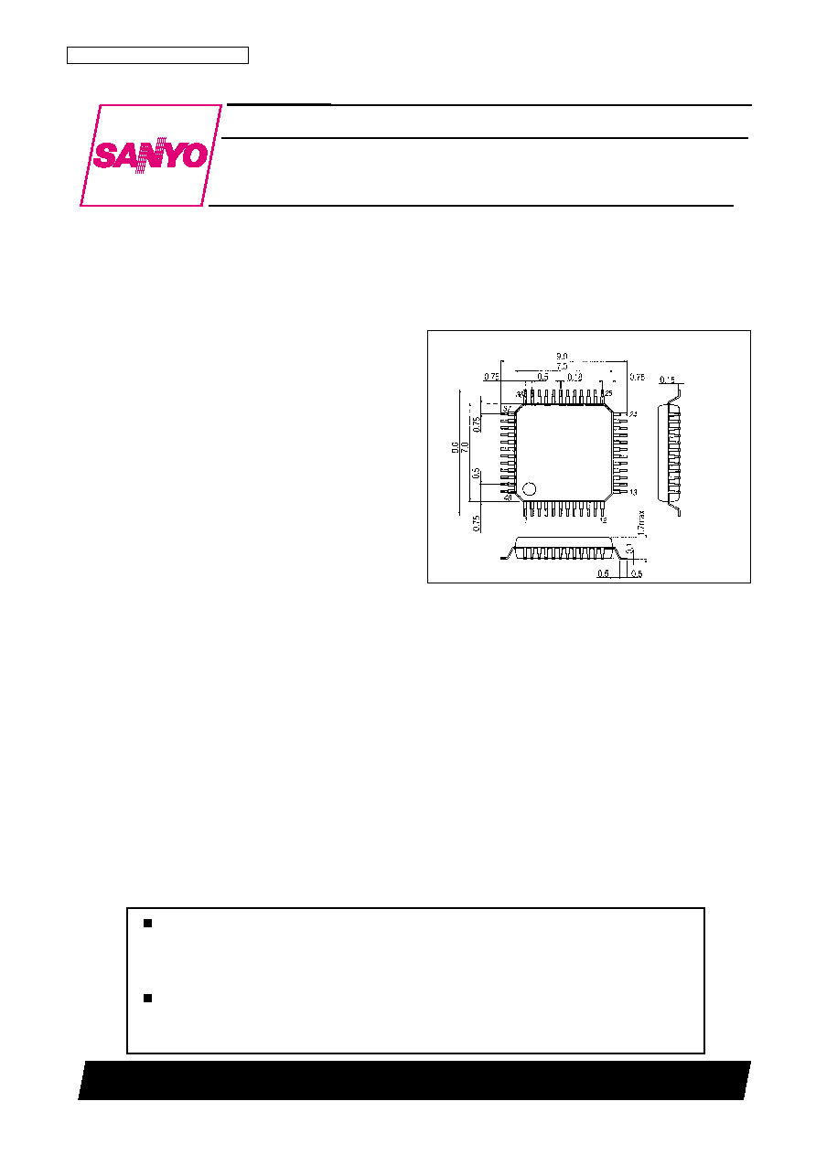
Package Dimensions
unit: mm
3163A-SQFP48
SANYO: SQFP48
[LA9605W]
LA9605W
SANYO Electric Co.,Ltd. Semiconductor Bussiness Headquarters
TOKYO OFFICE Tokyo Bldg., 1-10, 1 Chome, Ueno, Taito-ku, TOKYO, 110-8534 JAPAN
MD Player RF and Matrix Signal-Processing IC
Monolithic Linear IC
Any and all SANYO products described or contained herein do not have specifications that can handle
applications that require extremely high levels of reliability, such as life-support systems, aircraft's
control systems, or other applications whose failure can be reasonably expected to result in serious
physical and/or material damage. Consult with your SANYO representative nearest you before using
any SANYO products described or contained herein in such applications.
SANYO assumes no responsibility for equipment failures that result from using products at values that
exceed, even momentarily, rated values (such as maximum ratings, operating condition ranges, or other
parameters) listed in products specifications of any and all SANYO products described or contained
herein.
No. 5980-2/11
LA9605W
Parameter
Symbol
Conditions
Ratings
Unit
Maximum supply voltage
V
CC
max
7
V
Allowable power dissipation
Pd max
When mounted on a 114.3
◊
76.1
◊
1.6-mm single-sided
350
mW
glass-epoxy printed circuit board. Ta
75 ∞C
Operating temperature
Topr
≠25 to +75
∞C
Storage temperature
Tstg
≠40 to +150
∞C
Specifications
Maximum Ratings
at Ta = 25∞C
Parameter
Symbol
Conditions
Ratings
Unit
Recommended supply voltage
V
CC
5
V
Operating supply voltage range
V
CC
op
2.7 to 5.5
V
Operating Conditions
at Ta = 25∞C
Parameter
Symbol
Conditions
Ratings
Unit
min
typ
max
Current drain
I
CC
18
32
46
mA
[RF AMP GROVE]
Gain
VG
RFMG
1 EQ
O
/I : J = V
C
27
30
33
dB
[RF AMP MO.PIT]
Offset
V
OS RFMP
1 RF
O
1 : I = J = V
C
V
C
≠ 245
V
C
≠ 185
V
C
≠ 125
mV
Gain
VG
RFMP
1 EQ
O
/I : I = J
15
18
21
dB
[RF AMP AL]
Offset
V
OS RFAP
1 RF
O
1 : I = J = V
C
V
C
≠ 152
V
C
≠ 92
V
C
≠ 32
mV
Gain
VG
RFAP
1
EQ
O
/I : I = J = V
C
5.5
8.5
11.5
dB
[RF AMP]
Output level
H
V
ORFH
1
EQ
O
: RFI1 = V
C
+ 1 V
3.5
4.1
V
L
V
ORFL
1
EQ
O
: RFI1 = V
C
≠ 1 V
0.9
1.5
V
[ABCD GR]
Gain
VG
ABG
1
ABCD/A (10 kHz) : A = B = C = D, SGC = 0.78 V
17.5
20.5
23.5
dB
Output level
H
V
OABGH
2
ABCD : A = B = C = D = V
C
≠ 400 mV, SGC = 0.78 V
4.5
4.9
V
L
V
OABGL
2
ABCD : A = B = C = D = V
C
+ 400 mV, SGC = 0.78 V
0.1
0.5
V
[ABCD PIT]
Gain
VG
ABP
1
ABCD/A (10 kHz) : A = B = C = D, SGC = 0.3 V
10.6
13.6
16.6
dB
Frequency characteristics
V
G
ABP
1
ABCD/A (10 kHz) ≠ ABCD/A (35 kHz), SGC = 0.3 V
3.9
6.9
9.9
dB
[FOCS]
Output level
H
V
OFOH
1
FE : B = D = V
C
+ 825 mV, A = C = V
C
, SGC = 0.3 V
4.5
4.9
V
L
V
OFOL
1
FE : B = D = V
C
≠ 825 mV, A = C = V
C
, SGC = 0.3 V
0.1
0.5
V
Gain
V
GFO
1
FE/A (5 kHz) : A = ≠B = C = ≠D, SGC = 0.3 V
13.9
16.9
19.9
dB
Frequency characteristics
V
GFO
1
FE/A (5 kHz) ≠ FE/A (26 kHz) : A = ≠B = C = ≠D,
0.4
3.4
6.4
dB
SGC = 0.3 V
[TE GR]
Output level
H
V
OTEGH
1
TE : F = V
C
+ 200 mV, E = V
C
, SGC = 0.78 V
4.5
4.9
V
L
V
OTEGL
1
TE : F = V
C
≠ 200 mV, E = V
C
, SGC = 0.78 V
0.1
0.5
V
Gain
VG
TEG
1
TE/E (5 kHz) : E = ≠F, SGC = 0.78 V
31.4
34.4
37.4
dB
Frequency characteristics
V
G
TEG
1 TE/E (5 kHz) ≠ TE/E (38 kHz) : E = ≠F, SGC = 0.78 V
1.8
4.8
8.8
dB
[TE PIT]
Gain
VG
TEP
1
TE/E (5 kHz) : E = ≠F, SGC = 0.3 V
25.2
28.2
31.2
dB
Frequency characteristics
V
G
TEP
1
TE/E (5 kHz) ≠ TE/E (38 kHz) : E = ≠F, SGC = 0.3 V
1.8
4.8
8.8
dB
[ADIP]
Output level
H
V
OADH
1
CAD : A = D = V
C
+ 0.4 V, B = C = V
C
1.4
1.7
2.0
V
L
V
OADL
1
CAD : A = D = V
C
≠ 0.4 V, B = C = V
C
3.1
3.3
3.6
V
Electrical Characteristics
at Ta = 25∞C, V
CC
= 5 V
Continued on next page.
No. 5980-3/11
LA9605W
Parameter
Symbol
Conditions
Ratings
Unit
min
typ
max
[APC LDON]
Output level
H
V
OLH
1
LD
D
: LD
REF
= 0 V, LD
S
= 1 V
3.7
4.2
4.7
V
L
V
O LL
1
LD
D
: LD
REF
= 1 V, LD
S
= 0 V
0.3
0.8
1.3
V
[APC LDOFF]
Off voltage
V
OLOF
1
LD
D
: LD
REF
= 1 V, LD
S
= 0 V
3.7
4.2
4.7
V
[HFL]
Output level
H
V
OHFLH
1
HFL : HFL
IN
= V
C
≠ 0.1 V
4.6
4.8
V
L
V
OHFLL
1
HFL : HFL
IN
= V
C
0.2
0.4
V
[DEFCT]
Output level
H
V
ODEFH
1
DFO : CC
I
= 1.5 V
4.6
4.9
V
L
V
ODEFL
1
DFO : CC
I
= OPEN, A = B = C = D = V
C
≠ 200 mV
0.1
0.4
V
[VC reference voltage]
VO
SC
V
C
:
2.35
2.5
2.65
V
VO
CLSO
V
C
: V
C
≠ 1 mA
2.35
2.5
2.65
V
VO
CLSI
V
C
: V
C
+ 1 mA
2.35
2.5
2.65
V
[PREPIT MO]
High-level output voltage
VO
PPH
1
PPIT : I = J = 200 kHz (95 mVp-p + V
C
+ 0.125 V)
4.6
4.8
V
Low-level output voltage
VO
PPL
1
PPIT : I = J = 30 kHz (95 mVp-p + V
C
+ 0.125 V)
0.2
0.4
V
High/low level switching time
DTPP1
PPIT : I = J = 200 kHz to 30 kHz
70
150
230
µs
(95 mVp-p + V
C
+ 0.125 V)
[BPF]
Gain
VG
BF
1
WO
O/A
(22.05 kHz) : A = ≠B = ≠C = D, SGC = 0.3 V
23.8
26.8
29.8
dB
Filter characteristics
VG
BF
2
VG
BF1
/VG
BF2
: (16 kHz), SGC = 0.3 V
0.8
4.8
9.8
dB
VG
BF
3
VG
BF1
/VG
BF3
: (30 kHz), SGC = 0.3 V
0.4
4.4
9.4
dB
[I ≠ V]
IV voltage A
V
RA
A : V (≠1 µA) ≠ V (≠2 µA)
70
100
130
mV
IV voltage B
V
RB
B : V (≠1 µA) ≠ V (≠2 µA)
70
100
130
mV
IV voltage C
V
RC
C : V (≠1 µA) ≠ V (≠2 µA)
70
100
130
mV
IV voltage D
V
RD
D : V (≠1 µA) ≠ V (≠2 µA)
70
100
130
mV
IV voltage E
V
RE
E : V (≠1 µA) ≠ V (≠2 µA)
70
100
130
mV
IV voltage F
V
RF
F : V (≠1 µA) ≠ V (≠2 µA)
70
100
130
mV
Ta = 25∞C, V
CC
= 2.7 V
[FOCS]
Offset
V
OSFO
1
FE : A = B = C = D = OPEN, SGC = 0.78 V
≠300
0
+300
mV
[COMP]
Offset
V
OSCO
1
WO
I
: WO
I
= OPEN
≠15
0
+15
mV
Continued from preceding page.
Test Circuit
No. 5980-4/11
LA9605W
No. 5980-5/11
LA9605W
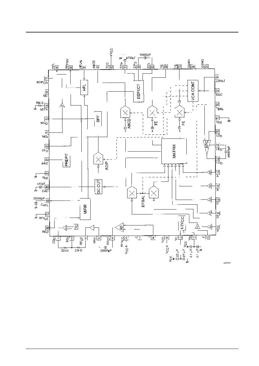
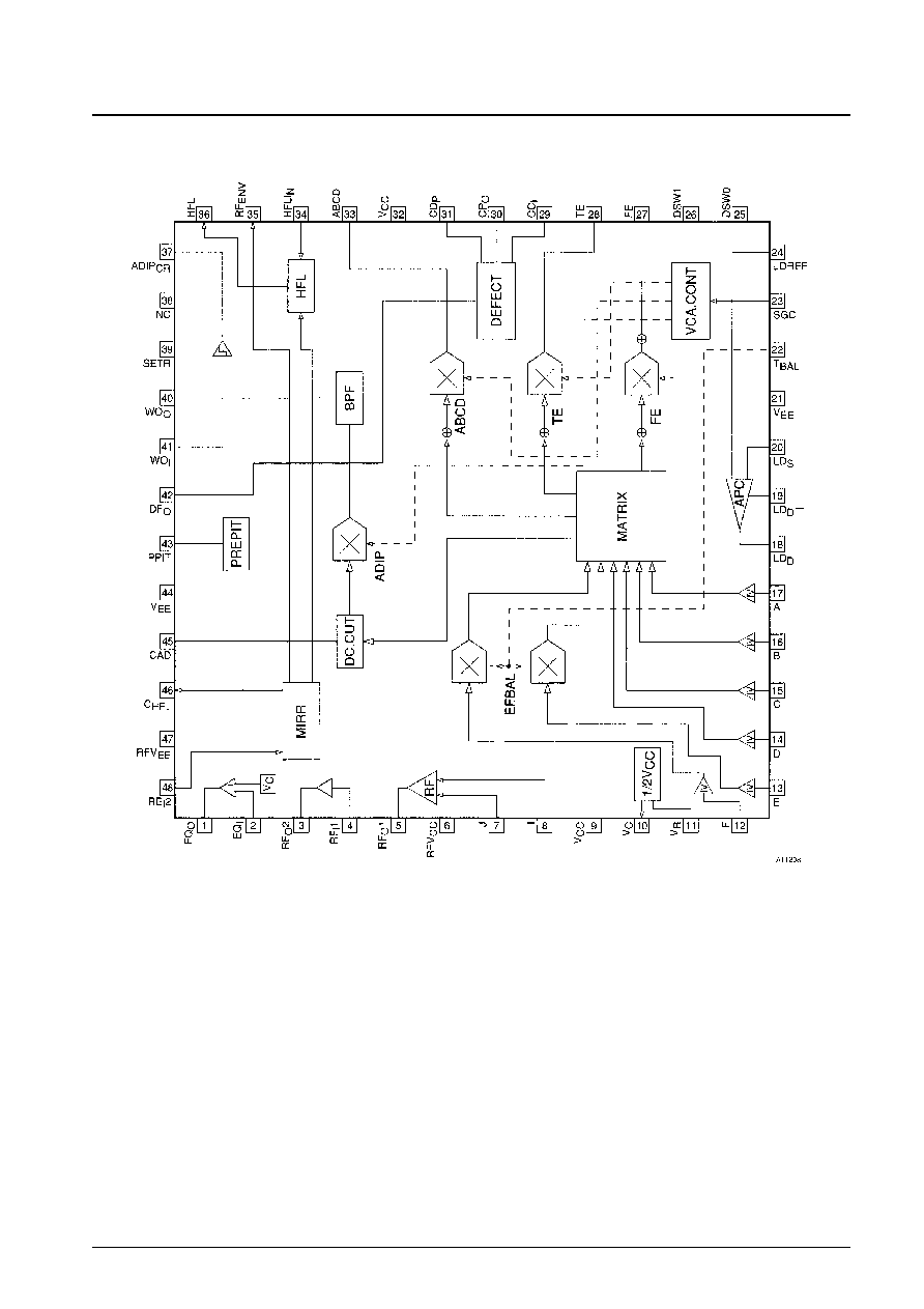
Block Diagram and Pin Assignment
No. 5980-6/11
LA9605W
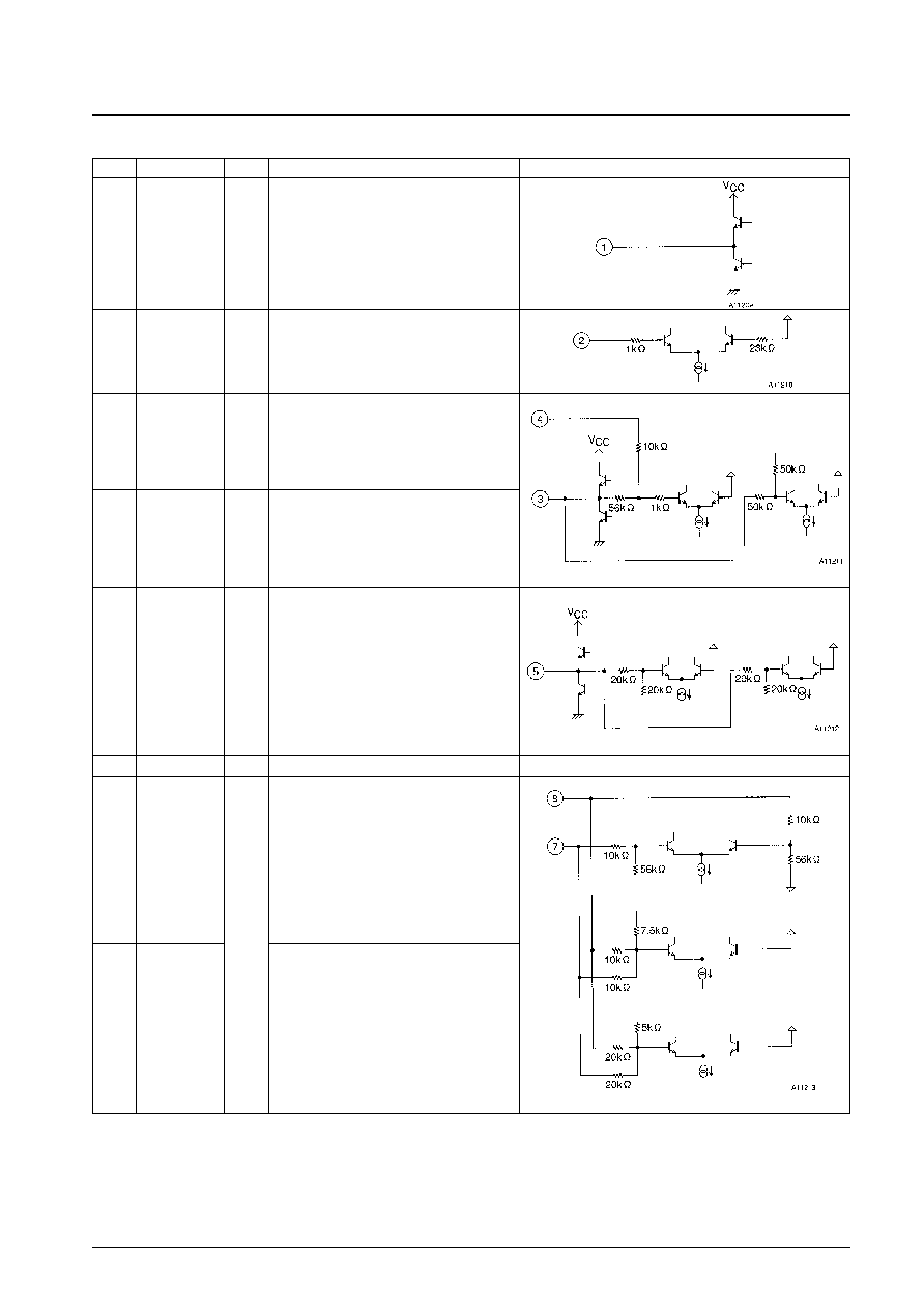
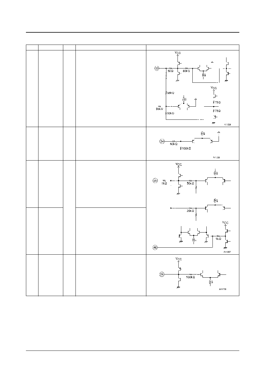
Pin Functions
Pin No.
Pin
I/O
Function
Equivalent circuit
RF equalizer output
1
EQ
O
O
RF equalizer input
2
EQ
I
I
RF output
3
RF
O
2
O
RF AC coupled input
4
RF
I
1
I
RF AC coupled output
RF block power supply
I/V converted RF signal input
5
RF
O
1
O
6
RFV
CC
P
7
J
I
I/V converted RF signal input
8
I
Continued on next page.
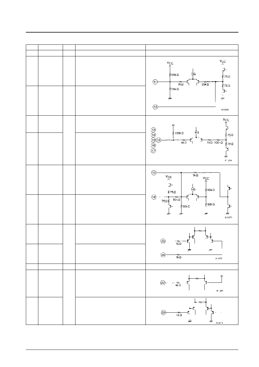
No. 5980-7/11
LA9605W
Continued from preceding page.
Pin No.
Pin
I/O
Function
Equivalent circuit
Matrix block power supply
9
V
CC
P
1/2 V
CC
output (reference voltage)
10
V
C
O
1/2 V
CC
input
11
V
R
I
Side beam signal inputs
12
13
F
E
I
APC output
18
LD
D
O
I/V converted laser optical intensity input
20
LD
S
I
APC phase compensation capacitor connection
19
LD
D
≠
I
Laser power setting input
24
LD
REF
Matrix block ground
21
V
EE
P
Tracking error signal balance adjustment voltage
input
22
T
BAL
I
V
CA
gain control voltage input (ground reference)
23
SGC
Main beam signal inputs
14
15
16
17
D
C
B
A
Continued on next page.
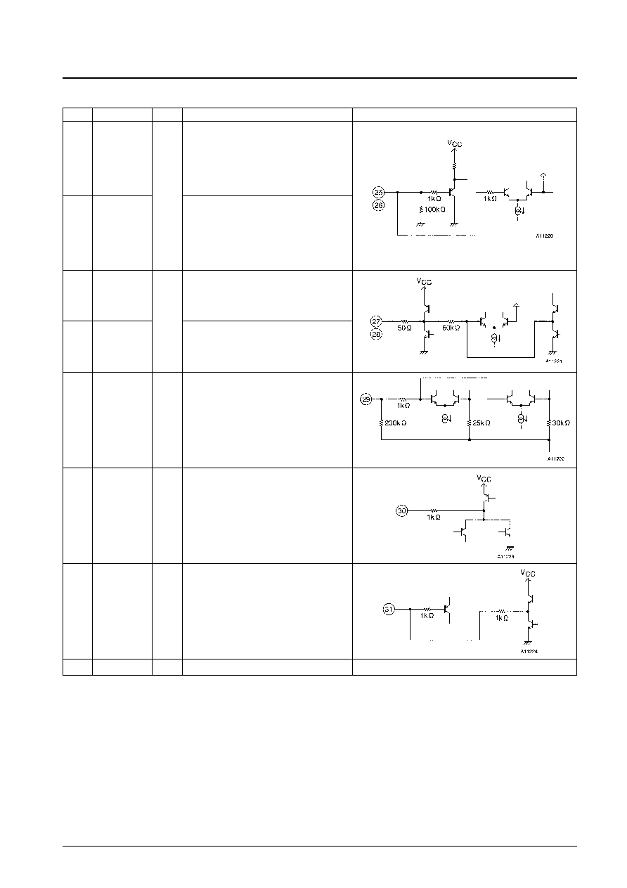
No. 5980-8/11
LA9605W
Continued from preceding page.
Pin No.
Pin
I/O
Function
Equivalent circuit
Disc mode switching signal input, laser off input
High: Low reflectance disc
Low: High reflectance disc
If both DSW0 and DSW1 are low, the laser is off.
25
DSW0
I
Focus error signal output
27
FE
O
Defect peak hold signal AC coupled input
29
CC
I
I
Defect peak hold signal output
30
CP
O
O
Defect peak hold capacitor connection
31
C
DP
O
ADIP block power supply
32
V
CC
P
Tracking error signal output
28
TE
Disc mode switching signal input, laser off input
High: Tracking is over a pit
Low: Tracking is over a groove
If both DSW0 and DSW1 are low, the laser is off.
26
DSW1
Continued on next page.
No. 5980-9/11
LA9605W
Continued from preceding page.
Pin No.
Pin
I/O
Function
Equivalent circuit
Main beam optical intensity signal output
33
ABCD
O
HFL detection optical intensity signal AC coupled
input used in groove mode
34
HFL
IN
I
RF envelope signal output
35
RF
ENV
O
HFL signal (tracking on/off signal) output
36
HFL
O
Mirror peak hold capacitor connection
46
C
HFL
Continued on next page.

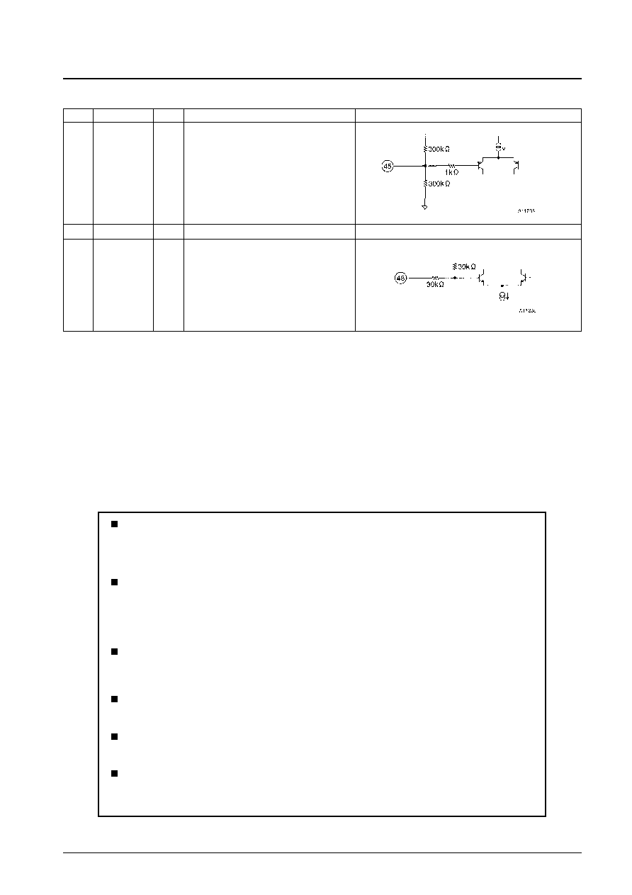
No. 5980-10/11
LA9605W
Continued from preceding page.
Pin No.
Pin
I/O
Function
Equivalent circuit
ADIP carrier output
37
ADIP
CR
O
No connection
38
NC
--
Bandpass filter fo setting
39
SETR
I
Wobble signal output
40
WO
O
O
Wobble signal AC coupled input
41
WO
I
I
Defect detection signal output
42
DF
O
O
Pit/groove
43
PPIT
O
ADIP block ground
44
V
EE
P
Continued on next page.
PS No. 5980-11/11
LA9605W
This catalog provides information as of December, 1998. Specifications and information herein are
subject to change without notice.
Specifications of any and all SANYO products described or contained herein stipulate the performance,
characteristics, and functions of the described products in the independent state, and are not guarantees
of the performance, characteristics, and functions of the described products as mounted in the customer's
products or equipment. To verify symptoms and states that cannot be evaluated in an independent device,
the customer should always evaluate and test devices mounted in the customer's products or equipment.
SANYO Electric Co., Ltd. strives to supply high-quality high-reliability products. However, any and all
semiconductor products fail with some probability. It is possible that these probabilistic failures could
give rise to accidents or events that could endanger human lives, that could give rise to smoke or fire,
or that could cause damage to other property. When designing equipment, adopt safety measures so
that these kinds of accidents or events cannot occur. Such measures include but are not limited to protective
circuits and error prevention circuits for safe design, redundant design, and structural design.
In the event that any or all SANYO products (including technical data, services) described or contained
herein are controlled under any of applicable local export control laws and regulations, such products must
not be exported without obtaining the export license from the authorities concerned in accordance with the
above law.
No part of this publication may be reproduced or transmitted in any form or by any means, electronic or
mechanical, including photocopying and recording, or any information storage or retrieval system,
or otherwise, without the prior written permission of SANYO Electric Co., Ltd.
Any and all information described or contained herein are subject to change without notice due to
product/technology improvement, etc. When designing equipment, refer to the "Delivery Specification"
for the SANYO product that you intend to use.
Information (including circuit diagrams and circuit parameters) herein is for example only; it is not
guaranteed for volume production. SANYO believes information herein is accurate and reliable, but
no guarantees are made or implied regarding its use or any infringements of intellectual property rights
or other rights of third parties.
Pin No.
Pin
I/O
Function
Equivalent circuit
Wobble DC cut capacitor connection
45
CAD
--
RF block ground
47
RFV
EE
P
RF signal input
48
RF
I
2
I
Continued from preceding page.