 | –≠–ª–µ–∫—Ç—Ä–æ–Ω–Ω—ã–π –∫–æ–º–ø–æ–Ω–µ–Ω—Ç: LB11650 | –°–∫–∞—á–∞—Ç—å:  PDF PDF  ZIP ZIP |
Ordering number : ENN7390
93003TN (OT) No. 7390-1/6
Overview
The LB11650 is a full bridge driver that supports
switching between forward and reverse directions. It
operates in one of four modes under application control:
forward, reverse, brake, and open. It also supports direct
PWM control from an external signal. The LB11650 is
optimal for driving brush DC motors and bipolar stepping
motors.
Features
∑ Supports PWM input
∑ Built-in high and low side diodes
∑ Simultaneous on state prevention function (prevents
through currents)
∑ Built-in thermal shutdown circuit (latching type)
∑ High and low side short circuit protection function
(latching type overcurrent protection)
∑ Externally controllable modes: forward, reverse, brake,
open
∑ Standby mode function
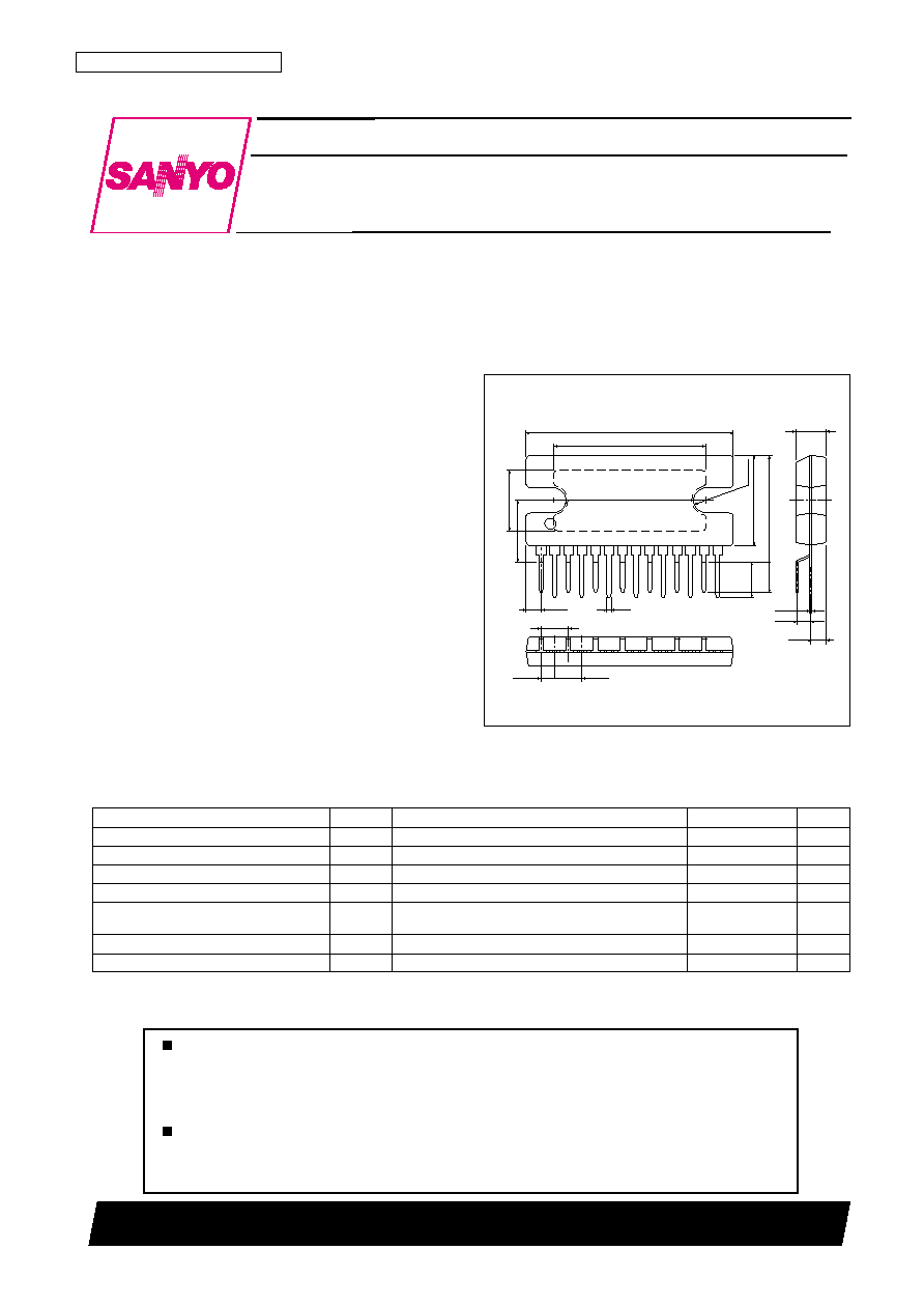
Package Dimensions
unit: mm
3113A-SIP14HZ
27.0
20.0
R1.7
0.5
1.94
8.4
7.8
14.5max
14
1
0.4
11.8
5.2
4.6
1.6
2.2
4.0
1.78
3.56
3.56
SANYO: SIP14HZ
[LB11650]
LB11650
SANYO Electric Co.,Ltd. Semiconductor Company
TOKYO OFFICE Tokyo Bldg., 1-10, 1 Chome, Ueno, Taito-ku, TOKYO, 110-8534 JAPAN
PWM Input Forward/Reverse Motor Driver
Monolithic Digital IC
Any and all SANYO products described or contained herein do not have specifications that can handle
applications that require extremely high levels of reliability, such as life-support systems, aircraft's
control systems, or other applications whose failure can be reasonably expected to result in serious
physical and/or material damage. Consult with your SANYO representative nearest you before using
any SANYO products described or contained herein in such applications.
SANYO assumes no responsibility for equipment failures that result from using products at values that
exceed, even momentarily, rated values (such as maximum ratings, operating condition ranges, or other
parameters) listed in products specifications of any and all SANYO products described or contained
herein.
Parameter
Symbol
Conditions
Ratings
Unit
Motor supply voltage
VM max
30
V
Peak output current
I
O
PEAK
tW
10 µs
2.0
A
Continuous output current
I
O
max
1.5
A
Logic system supply voltage
V
CC
max
7.0
V
Allowable power dissipation
Pd max
When mounted on a glass epoxy circuit board
3.5
W
(reference value): 114.3 mm
◊
76.1 mm
◊
1.6 mm
Operating temperature
Topr
≠20 to +85
∞C
Storage temperature
Tstg
≠55 to +150
∞C
Specifications
Absolute Maximum Ratings
at Ta = 25∞C

No. 7390-2/6
LB11650
Parameter
Symbol
Conditions
Ratings
Unit
Motor supply voltage
VM
8 to 28
V
Logic system supply voltage
V
CC
3.0 to 5.25
V
Logic input voltage range
V
IN
≠0.3 to V
CC
V
Recommended Operating Ranges
at Ta = 25∞C
Parameter
Symbol
Conditions
Ratings
Unit
min
typ
max
[Output Block]
Output stage supply current 1
IM ON
With no load, ST = high
0.84
1.2
1.56
mA
Output stage supply current 2
IM wt
With no load, ST = low
50
µA
Output saturation voltage 1
V
O
sat1
I
O
= +0.5 A, sink side
0.3
0.5
V
Output saturation voltage 2
V
O
sat2
I
O
= +1.0 A, sink side
0.5
0.7
V
Output saturation voltage 3
V
O
sat3
I
O
= ≠0.5 A, source side
1.5
1.8
V
Output saturation voltage 4
V
O
sat4
I
O
= ≠1.0 A, source side
1.7
2.0
V
Output leakage current
I
O
leak
V
O
= VM, sink side
50
µA
V
O
= 0 V, source side
≠50
µA
[Logic Block]
V
CC
= 5 V, with the R pin open
50
68
85
mA
I
CC
ON
BRAKE: LOW, PWM: HI, ST: HI
V
CC
= 3.3 V, with the R pin shorted to V
CC
55
75
95
mA
Logic supply current
BRAKE: LOW, PWM: HI, ST: HI
I
CC
BR
BRAKE: HI, PWM: HI, ST: HI
3.4
4.7
6.0
mA
I
CC
OFF
BRAKE: LOW, PWM: LOW, ST: HI
4.0
5.2
6.5
mA
I
CC
wt
ST: LOW
50
µA
Input voltage
VINH
2.0
V
VINL
0.8
V
Input current
IINH
V
IN
= 3.3 V
35
50
75
µA
IINL
V
IN
= 0.8 V
5
10
13
µA
C pin charge current
IC
VC = 0 V
35
50
65
µA
C pin output off threshold voltage
Vtc
1.17
1.3
1.43
V
VHS pin current detection
VtVHS
VM ≠ 0.55
VM ≠ 0.5
VM ≠ 0.45
V
threshold voltage
VLS pin current detection
VtVLS
0.45
0.5
0.55
V
threshold voltage
Low voltage cutoff voltage
VLVSD
2.25
2.5
2.75
V
Low voltage cutoff hysteresis
VLVHYS
0.15
0.2
0.25
V
Thermal shutdown temperature
TTSD
Design target value
*
150
175
∞C
Electrical Characteristics
at Ta = 25∞C, VM = 24 V, V
CC
= 5 V
*
: This is a design target value and is not measured.
Pd max -- Ta
4.0
3.5
3.0
2.5
2.0
1.5
1.0
0.5
0
≠20
0
20
40
60
80 85
100
Allowable power dissipation, Pdmax
--
W
Ambient temperature, Ta --
∞
C
ILB01548
Specified circuit board: 114.3
◊
76.1
◊
1.6 mm
Glass epoxy resin

Pin Assignment
No. 7390-3/6
LB11650
OA
1
2
3
4
5
6
7
8
9
10
11
12
13
14
Top view
VLS
VM
VHS
V
CC
ST
C
PWM
PHASE
BRAKE
GND
R
DiGND
OB
LB11650
Truth Table
X: H or L
PHASE
BRAKE
ST
PWM
OA
OB
Operating mode
H
L
H
H
H
L
Forward
L
L
H
H
L
H
Reverse
X
L
H
L
OFF
OFF
Output off
X
H
H
X
H
H
Brake
X
X
L or OPEN
X
OFF
OFF
Standby mode (circuits off)
Pin Functions
Pin No.
Pin
Pin function
1
OA
Output
14
OB
Output
4
VHS
High side current sensing (Insert an external resistor between VM and VHS. When the voltage across this resistor reaches 0.5 V,
the outputs are turned off.)
2
VLS
Low side current sensing (Insert an external resistor between VLS and ground. When the voltage across this resistor reaches
0.5 V, the outputs are turned off.)
7
C
Connection for an external filter capacitor that prevents incorrect operation of the current sensing output shutdown and thermal
shutdown circuits.
3
VM
Motor system power supply
5
V
CC
Logic system power supply
9
PHASE
Forward/reverse switching pin
10
BRAKE
Brake control input. A high input switches the IC to brake mode.
6
ST
Standby mode control. The IC operates in standby mode when this pin is low or open.
8
PWM
PWM input. High: on
Low: off
12
R
Low side drive current switching. (Short R to V
CC
when V
CC
is 3.3 V, and leave R open when V
CC
= 5.0 V.)
11
GND
Ground
13
DiGND
Lower side regeneration diode ground connection

High/Low Short Protection Function
This function turns the outputs off to prevent destruction of the IC if a problem such as an output pin being shorted to
VM or ground occurs and excessive current flows in the output transistors.
When an excessive current flows in an output transistor, a potential will occur across either the high side or the low side
current sense resistor. If that value exceeds the current detection threshold voltage, the capacitor connected to the C pin
starts to charge. Then, when the C pin voltage is charged to the output off threshold voltage, the output transistors are
turned off.
To restart the IC once it has gone to the output off state, either set the ST pin to the low level, or temporarily cut the V
CC
power supply, and then reapply power.
The overcurrent detection current setting can be set to an arbitrary level with the resistor inserted between VM and VHS
for current flowing in the high side output transistor, and with the resistor inserted between VLS and ground for current
flowing in the low side output transistor.
When the resistor connected to VHS or VLS pin is R (
), the detected current I (A) will be as follows.
I (A) = 0.5 (V) / R (
)
For example, if R is 0.5
, the detected current I will be 1 A.
This function is not an output current limiter function.
The detection current described above has the meaning that the short-circuit protection circuit begins to operate when a
current in excess of the detection current flows in the outputs. Therefore, if an output pin is shorted to VM or ground, the
maximum possible overcurrent that the output transistors are capable of will flow until the mask time set with the filter
circuit has elapsed. Designers must exert great care in designing the mask time setting.
Filter Circuit
To prevent the overcurrent protection and thermal shutdown circuits from operating incorrectly due to noise, the
LB11650 includes a circuit that sets a mask time so that when an abnormality is detected, it only turns the outputs off if
that state continues for a certain length of time.
When the capacitor connected between the C pin and ground is C (pF), the mask time T (µs) will be as follows.
T (µs) = 2.6
◊
10
≠2
◊
C (pF)
For example, if C is 50 pF, the mask time T will be 1.3 µs.
Low Side Transistor Drive Current Switching Pin
Since the lower side output transistor drive current is created from V
CC
, if the V
CC
power supply level is reduced, the
drive current will also be reduced. Therefore, the LB11650 is provided with a pin for switching the drive current so that
the LB11650 can provide the same drive current when used with 3.3 V specifications as it does when used with 5 V
specifications.
When V
CC
= 5 V: Leave the R pin open.
When V
CC
= 3.3 V: Short the R pin to V
CC
.
No. 7390-4/6
LB11650

Block Diagram
No. 7390-5/6
LB11650
R
Control logic
circuit
PWM
PHASE
ST
BRAKE
VM
OA
OB
C
GND
VLS
Thermal shutdown
circuit
UVLO
VREF
circuit
Filter
circuit
V
CC
VHS
Latch
circuit
DiGND
M
V
CC
= 5 V SW OPEN
V
CC
= 3.3 V SW ON
12
6
10
9
8
5
11
7
2
13
4
3
14
1

PS No. 7390-6/6
LB11650
This catalog provides information as of September, 2003. Specifications and information herein are
subject to change without notice.
Specifications of any and all SANYO products described or contained herein stipulate the performance,
characteristics, and functions of the described products in the independent state, and are not guarantees
of the performance, characteristics, and functions of the described products as mounted in the customer's
products or equipment. To verify symptoms and states that cannot be evaluated in an independent device,
the customer should always evaluate and test devices mounted in the customer's products or equipment.
SANYO Electric Co., Ltd. strives to supply high-quality high-reliability products. However, any and all
semiconductor products fail with some probability. It is possible that these probabilistic failures could
give rise to accidents or events that could endanger human lives, that could give rise to smoke or fire,
or that could cause damage to other property. When designing equipment, adopt safety measures so
that these kinds of accidents or events cannot occur. Such measures include but are not limited to protective
circuits and error prevention circuits for safe design, redundant design, and structural design.
In the event that any or all SANYO products (including technical data, services) described or contained
herein are controlled under any of applicable local export control laws and regulations, such products must
not be exported without obtaining the export license from the authorities concerned in accordance with the
above law.
No part of this publication may be reproduced or transmitted in any form or by any means, electronic or
mechanical, including photocopying and recording, or any information storage or retrieval system,
or otherwise, without the prior written permission of SANYO Electric Co., Ltd.
Any and all information described or contained herein are subject to change without notice due to
product/technology improvement, etc. When designing equipment, refer to the "Delivery Specification"
for the SANYO product that you intend to use.
Information (including circuit diagrams and circuit parameters) herein is for example only; it is not
guaranteed for volume production. SANYO believes information herein is accurate and reliable, but
no guarantees are made or implied regarding its use or any infringements of intellectual property rights
or other rights of third parties.