 | –≠–ª–µ–∫—Ç—Ä–æ–Ω–Ω—ã–π –∫–æ–º–ø–æ–Ω–µ–Ω—Ç: LB11817 | –°–∫–∞—á–∞—Ç—å:  PDF PDF  ZIP ZIP |
Ordering number :EN
*
6213A
63099RM (OT) No. 6213-1/10
Overview
The LB11817 is a spindle motor driver for use in slim-
shaped FDDs that use 5 V power supply.
Functions and Features
∑ Three-phase full-wave linear drive
∑ Low saturation voltage
∑ Built-in digital speed control
∑ Start/stop circuit (active low)
∑ Speed switching
∑ Current limiter
∑ Index processing circuit
∑ The index timing can be adjustment with a variable
resistor.
∑ Thermal protection circuit
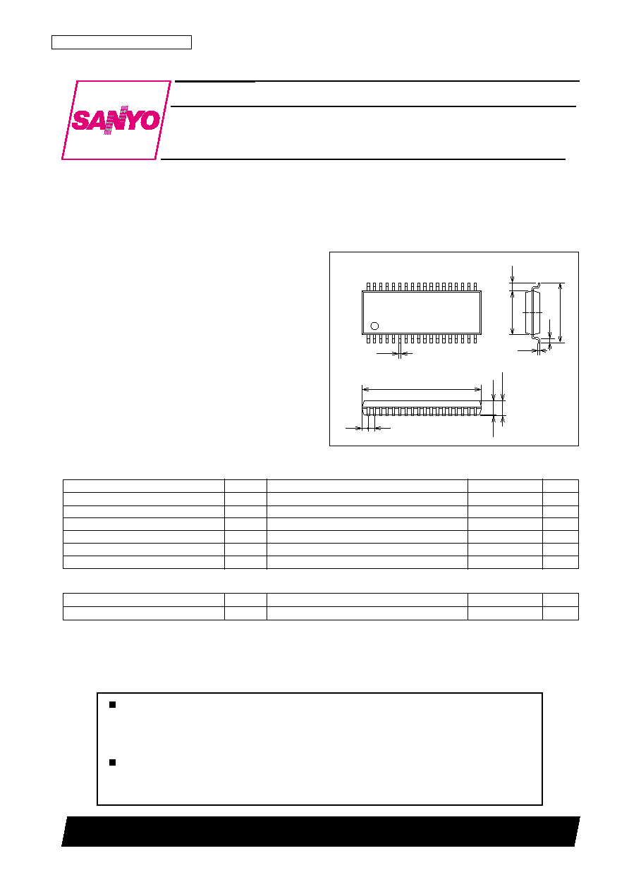
Package Dimensions
unit: mm
3247-SSOP36
1
36
18
19
0.8
15.2
0.5
7.6
0.20
0.30
0.8
5.6
1.0
(1.5)
1.8max
0.10
Preliminary
SANYO: SSOP36
[LB11817]
SANYO Electric Co.,Ltd. Semiconductor Company
TOKYO OFFICE Tokyo Bldg., 1-10, 1 Chome, Ueno, Taito-ku, TOKYO, 110-8534 JAPAN
Monolithic Digital IC
LB11817
Three-Phase Full-Wave Linear Drive
Any and all SANYO products described or contained herein do not have specifications that can handle
applications that require extremely high levels of reliability, such as life-support systems, aircraft's
control systems, or other applications whose failure can be reasonably expected to result in serious
physical and/or material damage. Consult with your SANYO representative nearest you before using
any SANYO products described or contained herein in such applications.
SANYO assumes no responsibility for equipment failures that result from using products at values that
exceed, even momentarily, rated values (such as maximum ratings, operating condition ranges, or other
parameters) listed in products specifications of any and all SANYO products described or contained
herein.
Parameter
Symbol
Conditions
Ratings
Unit
Maximum supply voltage
V
CC
max
7.0
V
Maximum output current
I
O max
1
t
0.5 s
1.5
A
Maximum steady-state output current
I
O max
2
1.0
A
Allowable power dissipation 1
Pdmax1
Independent IC
0.6
W
Operating temperature
Topr
≠20 to +80
∞C
Storage temperature
Tstg
≠40 to +150
∞C
Specifications
Absolute Maximum Ratings
at Ta = 25∞C
Parameter
Symbol
Conditions
Ratings
Unit
Supply voltage
V
CC
4.2 to 6.5
V
Allowable Operating Ranges
at Ta = 25∞C
No. 6213-2/10
LB11817
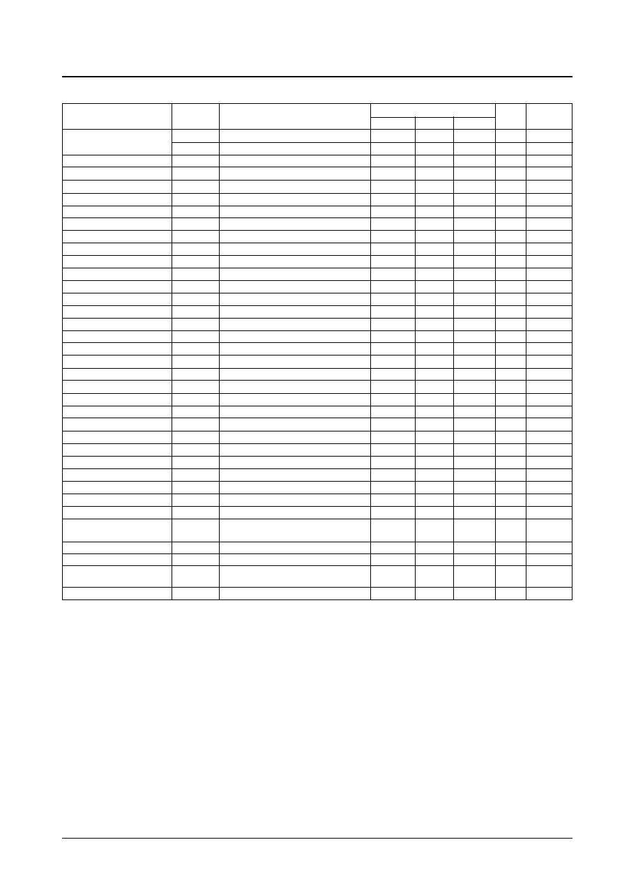
Electrical Characteristics
at Ta = 25∞C, V
CC
= 5 V
Note:
*
Items shown to be design target values are not measured.
Parameter
Symbol
Conditions
Ratings
Unit
Note
min
typ
max
Current drain
I
CCO
S/S = 5 V (standby mode)
10
µA
I
CC
S/S = 0 V (normal operation)
17
25
mA
SL bias current
I
SL
V
SL
= 0 V
10
µA
SL low-level input voltage
V
SLL
0
1.0
V
SL high-level input voltage
V
SLH
3.5
V
CC
V
S/S bias current
I
S/S
150
230
µA
S/S low voltage
V
S/SL
0
0.8
V
S/S high voltage
V
S/SH
3.5
V
CC
V
Hall amplifier input bias current
I
H
10
µA
Common-mode input voltage range
V
h
1.5
V
CC
≠ 1.0
V
Differential input voltage range
V
dif
50
200
mVp-p
Hall bias output voltage
V
HB
I
H
= 5 mA
0.5
0.8
1.1
V
Hall bias leakage current
I
HBL
S/S = 5 V
±10
µA
Output saturation voltage
V
sat
I
O
= 0.5 A sink+source
0.45
0.67
V
Output leakage current
I
OL
1.0
mA
Current limiter
V
lim
0.27
0.3
0.33
V
Control amplifier voltage gain
G
C
≠9
≠7
≠5
dB
Voltage gain inter-phase difference
G
C
±1
dB
V/I conversion source current
I
+
9
14
19
µA
V/I conversion sink current
I
≠
≠9
≠14
≠19
µA
V/I conversion current ratio
I
+
/I
≠
0.8
1.0
1.2
DSC buffer input current
I
DSC
1.0
µA
FG amplifier voltage gain
G
FG
48
dB
*
FG offset amplifier input
V
FG0
±10
mV
*
FG amplifier internal reference voltage
V
FGB
2.2
2.5
2.8
V
FG Schmitt hysteresis
Vsh
50
mV
*
Speed discriminator counts
N
1041.5
Discriminator operating frequency
F
D
1.1
MHz
*
Oscillator frequency range
F
OSC
1.1
MHz
*
Index output low-level voltage
V
IDL
I
O
= 2 mA
0.4
V
Index output leakage current
I
IDL
±10
µA
Index amplifier common-mode
V
ID
1.0
V
CC
≠ 1.0
V
input voltage range
Index input hysteresis
V
ID
25
mV
Boost voltage
VP
Ip = ≠5 mA
1.39
1.55
1.71
V
Thermal protection circuit
TSD
150
180
∞C
*
operating temperature
Hysteresis
TSD
40
∞C
*
No. 6213-3/10
LB11817
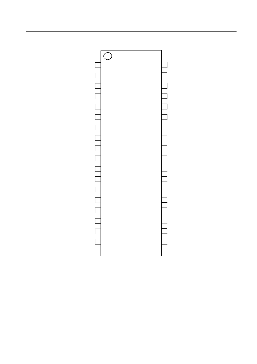
Pin Assignment
13
14
12
11
10
9
8
7
6
5
4
3
2
1
15
16
17
18
LB11817
19
20
21
22
23
24
25
26
27
30
28
29
31
32
33
34
35
36
I-
VR
I+
FG+
FG-
W-
W+
FGO
HB
V-
U-
U+
NC
NC
NC
UOUT
VOUT
PGND
WOUT
NC
D1
B1
B2
D2
V+
RF
VP
VCC
GND
DO
FC
CLK
SL
S/S
ID
TC
Top view
No. 6213-4/10
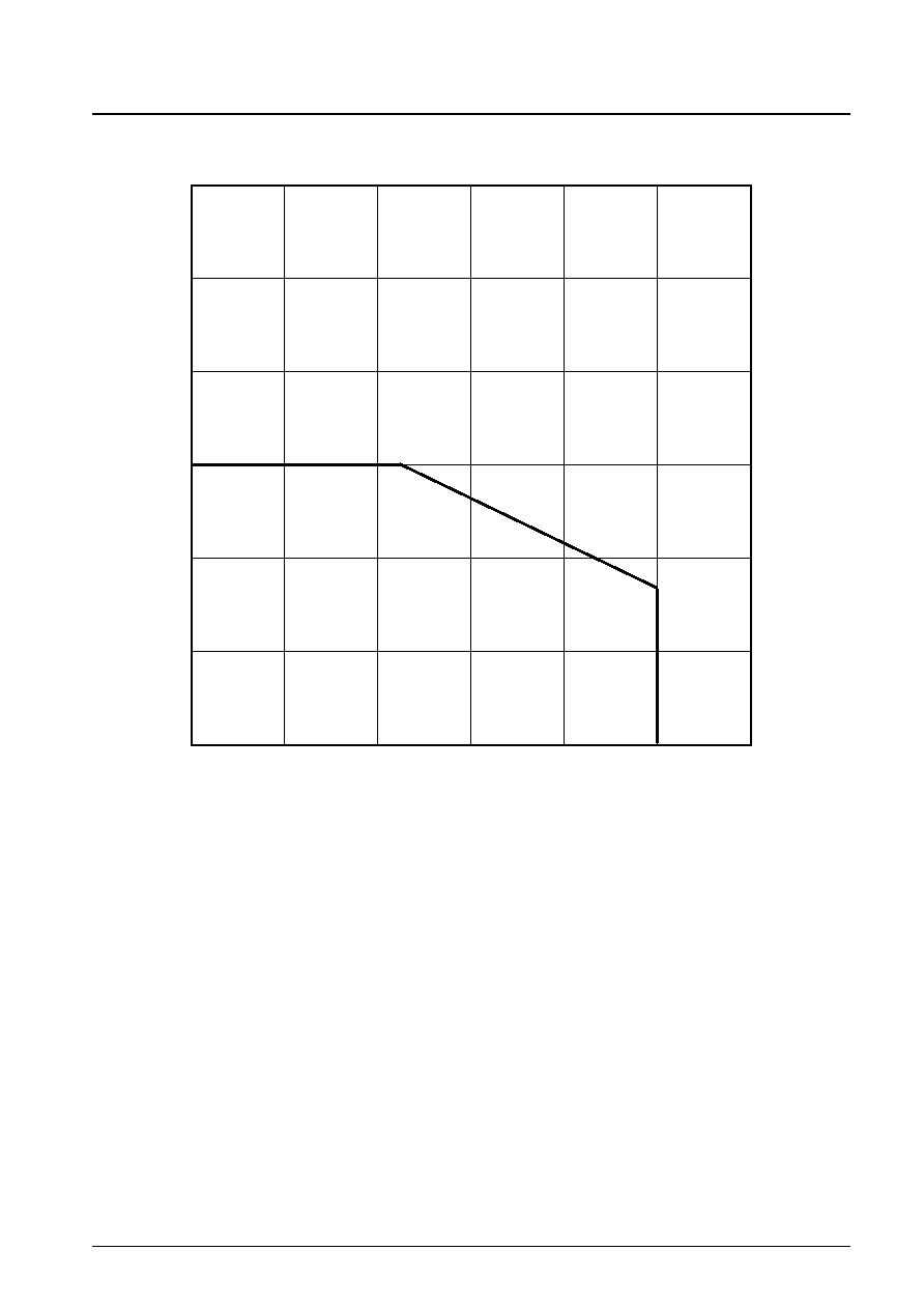
LB11817
100
80
60
40
20
0
0
-20
0.6
0.8
1.0
1.2
0.2
0.4
Allowable power dissipation, Pdmax (W)
Ambient temperature, Ta (∞C)
Independent IC
Pdmax -- Ta
No. 6213-5/10
LB11817
Truth Table
Source
sink
Hall input
U
V
W
1
V
W
H
H
L
2
V
U
L
H
L
3
W
U
L
H
H
4
W
V
L
L
H
5
U
V
H
L
H
6
U
W
H
L
L
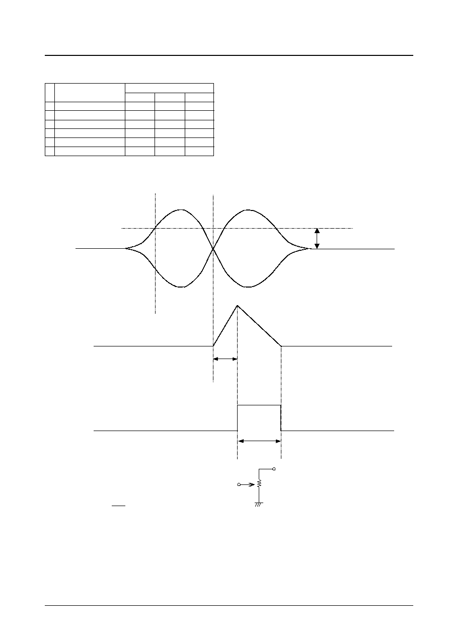
Index Delay Pulse Timing Chart
HYS
1
+
1
-
T1
T2
TC
ID
(V
VR
is the pin voltage)
T1
1.363 ms ........... SL = H
T1
1.635 ms ........... SL = L
T2
1.25
◊
T1
V
VR
FG+
VR
No. 6213-6/10
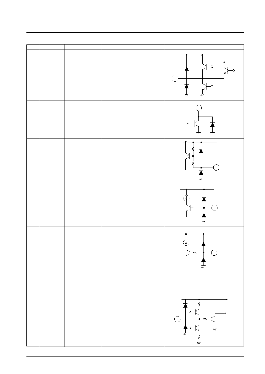
LB11817
Pin Functions
Pin No.
Symbol
Pin voltage
Function
Equivalent circuit
1
TC
1
Continued on next page.
∑ Connection for the external capacitor
used to adjust the index timing.
L: 0.4 Vmax
H: 4.5 Vmin
2
ID
2
∑ Index output
L: 1.0 Vmax
H: 3.5 Vmin
3
S/S
3
V
CC
∑ Start/stop control.
This is an active-low input.
L: 1.0 Vmax
H: 3.5 Vmin
4
SL
4
V
CC
∑ Speed switching input
L: 0.5 Vmax
H: V
CC
≠ 1.0 Vmin
5
CLK
2 k
V
CC
5
∑ Reference clock input.
The threshold voltage is 1.25 V. At
1 MHz, the LB11817 supports speeds of
300 and 360 rpm.
6
7
FC
DO
∑ Speed discriminator
V
CC
7
∑ Frequency characteristics correction.
Oscillation in the current control closed-
loop circuit can be stopped by inserting a
capacitor between this pin and ground.
No. 6213-7/10
LB11817
Pin No.
Symbol
Pin voltage
Function
Equivalent circuit
8
GND
Continued on next page.
4.2 to 6.5 V
9
V
CC
∑ Supply voltage
This voltage must be stabilized so that
ripple and noise do not enter the IC.
V
CC
+ 1.55 Vtyp
(Ip = ≠5 mA)
10
VP
∑ Boosted voltage output
Used as the output transistor pre-driver
power supply. This boosted voltage is
used when a low saturation output is
provided. In all other cases this pin will
be at the V
CC
potential.
11
RF
∑ Output current detection
An RF resistor inserted between this pin
and V
CC
converts the output current to the
voltage used for output current detection.
The current limiter circuit operates by
detecting the voltage on this pin.
12
15
D2
D1
VP
V
CC
15
12
∑ Connections for the two diodes used by
the voltage boost function.
13
14
17
19
20
B2
B1
W
OUT
V
OUT
U
OUT
∑ W-phase output
∑ V-phase output
∑ U-phase output
20
17
19
11
18
∑ Boost function switching circuit outputs 1
and 2
Continued from preceding page.
∑ Ground
This pin and pin 34 must all be
connected to the frame ground.
V
CC
14
13
10
10
10
10
No. 6213-8/10
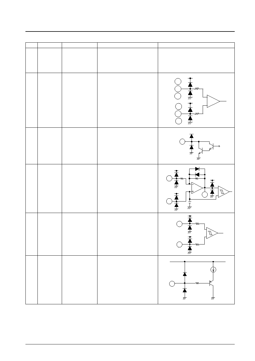
LB11817
Pin No.
Symbol
Pin voltage
Function
Equivalent circuit
18
PGND
1.5 Vmin
V
CC
≠ 1.0 Vmax
24
25
26
27
28
29
U
IN
+
U
IN
≠
V
IN
+
V
IN
≠
W
IN
+
W
IN
≠
∑ U-phase Hall device inputs
∑ V-phase Hall device inputs
∑ W-phase Hall device inputs
0.8 Vtyp
(IH = 5 mA)
30
HB
∑ Negative potential that provides Hall
device bias current
In the stopped state, this pin is set to the
open state to cut off the Hall device bias
current.
31
32
33
FGO
FG+
FG≠
∑ FG amplifier output
∑ FG amplifier minus input
∑ FG amplifier plus input
A 2.5 V reference voltage is generated
internally by the IC.
34
35
I+
I≠
V
cc
V
cc
35
34
200
200
∑ Index inputs
36
VR
∑ Index timing adjustment voltage input
Continued from preceding page.
∑ Output transistor ground
36
24
26
28
27
25
29
V
cc
V
cc
1k
1k
2.5 Vtyp
30
31
V
cc
V
CC
2. 5V
V
cc
32
33
750 k
3 k
No. 6213-9/10
LB11817
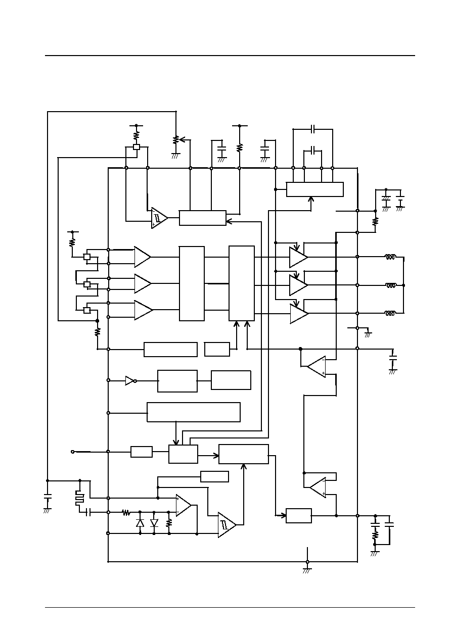
Block Diagram
Note that the values of the external components shown here are reference values and are not guaranteed to be appropriate
in a given application.
3 k
V
CC
S/S
SL
U+
U-
V+
V-
W+
W-
HB
W
V
U
W
V
U
25 mV
TC
50 mV
CLK
FG+
FG-
FGO
GND
DO
RF
U
V
1
V
CC
FC
0.1
µ
F
W
PG
I+
I-
ID
V
CC
VR
VP
D1 D2
B2
B1
V
CC
0.47
µ
F
0.1
0.1
0.1
0.1
µ
F
µ
F
µ
F
µ
F
µ
F
100 k
FG
pattern
Control amplifier and
current limiter
Timing adjustment
Hall amplifier
Hall bias
Chip select
Matrix
Amplitude control
Reference
voltage
300/360 rpm selection
Divider
Speed discriminator
FG
amplifier
(
◊
250)
Voltage boost circuit
OSC
TSD
Vref
V/I
PS No.6213-10/10
LB11817
This catalog provides information as of June, 1999. Specifications and information herein are subject to
change without notice.
Specifications of any and all SANYO products described or contained herein stipulate the performance,
characteristics, and functions of the described products in the independent state, and are not guarantees
of the performance, characteristics, and functions of the described products as mounted in the customer's
products or equipment. To verify symptoms and states that cannot be evaluated in an independent device,
the customer should always evaluate and test devices mounted in the customer's products or equipment.
SANYO Electric Co., Ltd. strives to supply high-quality high-reliability products. However, any and all
semiconductor products fail with some probability. It is possible that these probabilistic failures could
give rise to accidents or events that could endanger human lives, that could give rise to smoke or fire,
or that could cause damage to other property. When designing equipment, adopt safety measures so
that these kinds of accidents or events cannot occur. Such measures include but are not limited to protective
circuits and error prevention circuits for safe design, redundant design, and structural design.
In the event that any or all SANYO products (including technical data, services) described or contained
herein are controlled under any of applicable local export control laws and regulations, such products must
not be exported without obtaining the export license from the authorities concerned in accordance with the
above law.
No part of this publication may be reproduced or transmitted in any form or by any means, electronic or
mechanical, including photocopying and recording, or any information storage or retrieval system,
or otherwise, without the prior written permission of SANYO Electric Co., Ltd.
Any and all information described or contained herein are subject to change without notice due to
product/technology improvement, etc. When designing equipment, refer to the "Delivery Specification"
for the SANYO product that you intend to use.
Information (including circuit diagrams and circuit parameters) herein is for example only; it is not
guaranteed for volume production. SANYO believes information herein is accurate and reliable, but
no guarantees are made or implied regarding its use or any infringements of intellectual property rights
or other rights of third parties.