LB11847
No. 6183-1/16
LB11847
PWM Current Control Type Stepping Motor Driver
Monolithic Digital IC
The LB11847 is a driver IC for stepping motors
with PWM current control bipolar drive (fixed OFF
time). A special feature of this IC is that V
REF
voltage is constant while the current can be set in
15 steps, allowing drive of motors ranging from 1-
2 phase exciter types to 4W 1-2 phase exciter
types. The current decay pattern can also be
selected (SLOW DECAY, FAST DECAY, MIX
DECAY) to increase the decay of regenerative
current at chopping OFF, thereby improving
response characteristics. This is especially useful
for carriage and paper feed stepping motors in
printers and similar applications where high-
precision control and low vibrations are required.
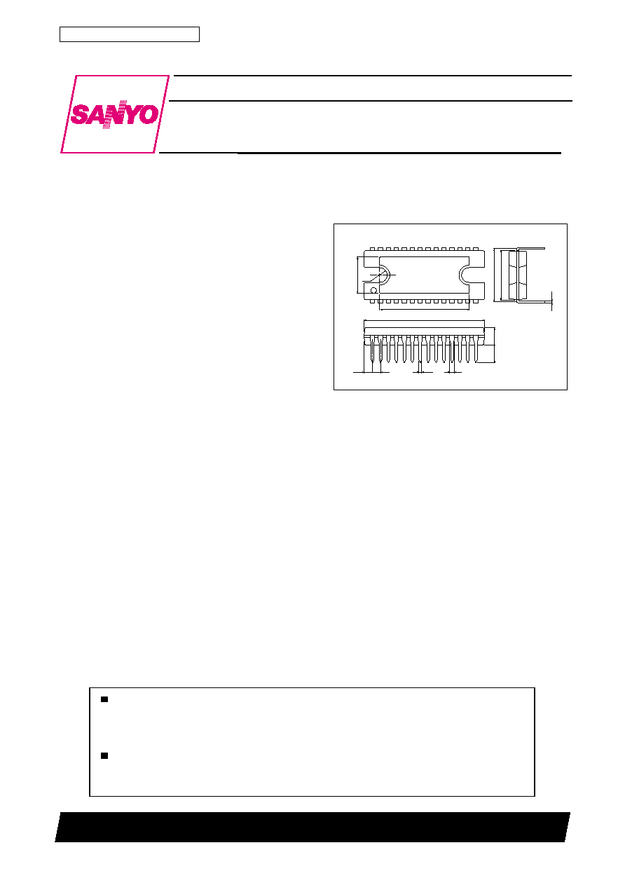
Package Dimensions
unit: mm
3147B-DIP28H
Overview
SANYO : DIP28H
[LB11847]
Features
� PWM current control (fixed OFF time)
� Load current digital selector (1-2, W1-2, 2W1-2, 4W1-2 phase exciter drive possible)
� Selectable current decay pattern (SLOW DECAY, FAST DECAY, MIX DECAY)
� Simultaneous ON prevention function (feedthrough current prevention)
� Noise canceler
� Built-in thermal shutdown circuit
� Built-in logic low-voltage OFF circuit
Ordering number : EN*6183
61199RM(KI)
1
14
28
15
0.4
0.6
4.0
4.0
27.0
20.0
R1.7
8.4
1.93
1.78
1.0
12.7
11.2
Any and all SANYO products described or contained herein do not have specifications that can handle
applications that require extremely high levels of reliability, such as life-support systems, aircraft's
control systems, or other applications whose failure can be reasonably expected to result in serious
physical and/or material damage. Consult with your SANYO representative nearest you before using
any SANYO products described or contained herein in such applications.
SANYO assumes no responsibility for equipment failures that result from using products at values that
exceed, even momentarily, rated values (such as maximum ratings, operating condition ranges, or other
parameters) listed in products specifications of any and all SANYO products described or contained
herein.
Preliminary
SANYO Electric Co.,Ltd. Semiconductor Company
TOKYO OFFICE Tokyo Bldg., 1-10, 1 Chome, Ueno, Taito-ku, TOKYO, 110-8534 JAPAN
LB11847
No. 6183-2/16
Absolute Maximum Ratings
at Ta = 25
�
C
Specifications
Allowable Operating Ranges
at Ta = 25
�
C
I
OPEAK
I
O
max
V
BB
t
W
20
�
s
V
E
V
IN
V
CC
�0.3 to V
CC
Parameter
Symbol
Conditions
Ratings
Unit
Motor supply voltage range
10 to 45
V
Logic supply voltage range
4.75 to 5.25
V
Reference voltage range
0.0 to 3.0
V
V
BB
V
CC
V
REF
Parameter
Symbol
Conditions
Ratings
Unit
Motor supply voltage
50
V
Output peak current
1.75
A
Output continuous current
1.5
A
Logic supply voltage
7.0
V
Logic input voltage range
V
Emitter output voltage
1.0
V
Allowable power dissipation
Pd max
Ta = 25
�
C
3.0
W
With heat sink
20
W
Operating temperature
Topr
�20 to +85
�
C
Storage temperature
Tstg
�55 to +150
�
C
0
�20
20
40
60
80
100
5
10
15
25
20
0
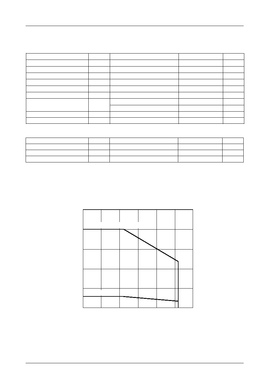
Ambient temperature, Ta � �C
Allowable power dissipation, Pd
max � W
Pd max � Ta
IC only
10.4
1.56
20.0
3.0
With an arbitrary large heat sink
LB11847
No. 6183-5/16
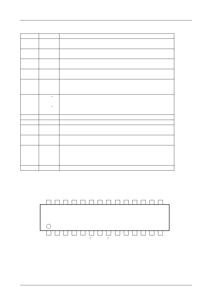
Pin Assignment
Pin Function
V
REF
1
V
REF
2
OUT
A
OUT
A
OUT
B
OUT
B
V
BB
I
A
4, I
A
3
I
A
2, I
A
1
I
B
4, I
B
3
I
B
2, I
B
1
V
CC
1
28
2
27
3
26
4
25
5
24
6
23
7
22
8
21
9
20
10
19
11
18
12
17
13
16
14
15
V
CC
PHASE1
ENABLE1
I A
1
I A
2
I A
3
I A
4
I B
4
I B
3
I B
2
I B
1
ENABLE2
PHASE2
GND
MD
V
REF
1
CR1
E1
DECAY1
OUT
A
OUT
A
OUT
B
OUT
B
DECAY2
E2
CR2
V
REF
2
V
BB
LB11847
A12533
Top view
Pin number
Pin name
Function description
Sets the OFF time for FAST mode and SLOW mode in MIX DECAY
Setting input range: 4V to 1.5V
2
Output set current reference supply pins
13
Setting voltage range: 0V to 3V
3
CR1
12
CR2
4
E1
11
E2
5
DECAY1
SLOW mode/FAST mode selector pins
10
DECAY2
SLOW DECAY: H
FAST DECAY: L
6
7
8
9
14
Output stage supply voltage pin
15
GND
Ground pin
27
PHASE1
16
PHASE2
26
ENABLE1
17
ENABLE2
22, 23
24, 25
Output set current digital input pins
21, 20
15-stage voltage setting
19, 18
28
Logic block supply voltage pin
1
M D
Output OFF time setting pins for switching operation
Pins for controlling the set current with sensing resistor RE
Output pins
Output phase selector input pins
Output ON/OFF setting input pins