 | –≠–ª–µ–∫—Ç—Ä–æ–Ω–Ω—ã–π –∫–æ–º–ø–æ–Ω–µ–Ω—Ç: LB11870 | –°–∫–∞—á–∞—Ç—å:  PDF PDF  ZIP ZIP |
Ordering number : ENN7256
80102AS (OT) No. 7256 -1/14
Overview
The LB11870 is a three-phase brushless motor driver
developed for driving the motors used with the polygonal
mirror in laser printers and plain paper copiers. It can
implement, with a single IC chip, all the circuits required
for polygonal mirror drive, including speed control and
driver functions. The LB11870 can implement motor drive
with minimal power loss due to its use of direct PWM
drive.
Functions and Features
∑ Three-phase bipolar drive
∑ Direct PWM drive
∑ Includes six high and low side diodes on chip.
∑ Output current control circuit
∑ PLL speed control circuit
∑ Phase lock detection output (with masking function)
∑ Includes current limiter, thermal protection, rotor
constraint protection, and low-voltage protection circuits
on chip.
∑ Deceleration type switching circuit (free running or
reverse torque)
∑ PWM oscillator
∑ Power saving circuit
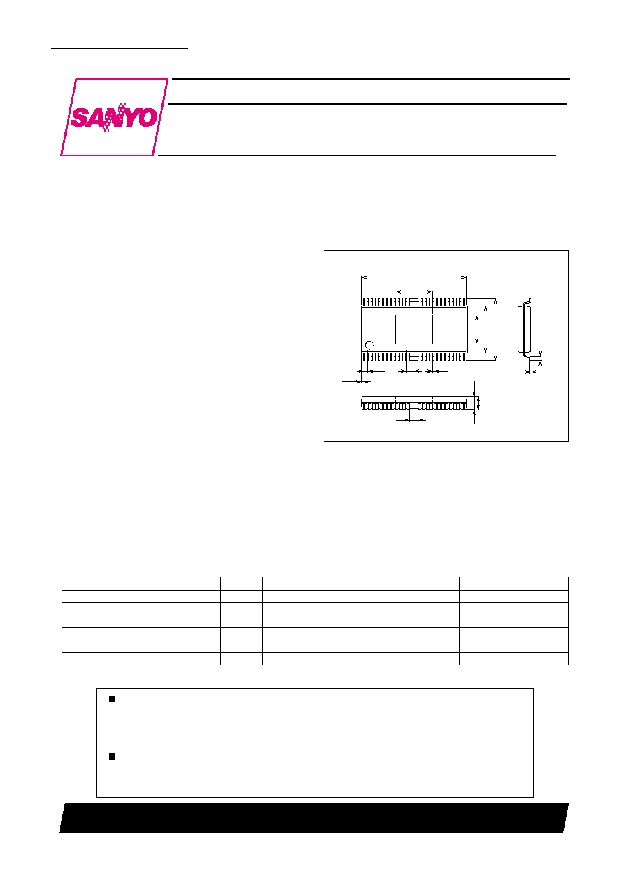
Package Dimensions
unit: mm
3265-HSSOP48
17.8
10.5
0.65
7.9
(4.9)
0.1
2.4max
(2.2)
(6.2)
0.2
1.5
0.65
(0.45)
1.3
0.2
1
24
25
48
SANYO: HSSOP48 (375 mil)
[LB11870]
LB11870
SANYO Electric Co.,Ltd. Semiconductor Company
TOKYO OFFICE Tokyo Bldg., 1-10, 1 Chome, Ueno, Taito-ku, TOKYO, 110-8534 JAPAN
Three-Phase Brushless Motor Driver
for Polygonal Mirror Motors
Monlithic Digital IC
Any and all SANYO products described or contained herein do not have specifications that can handle
applications that require extremely high levels of reliability, such as life-support systems, aircraft's
control systems, or other applications whose failure can be reasonably expected to result in serious
physical and/or material damage. Consult with your SANYO representative nearest you before using
any SANYO products described or contained herein in such applications.
SANYO assumes no responsibility for equipment failures that result from using products at values that
exceed, even momentarily, rated values (such as maximum ratings, operating condition ranges, or other
parameters) listed in products specifications of any and all SANYO products described or contained
herein.
Parameter
Symbol
Conditions
Ratings
Unit
Supply voltage
V
CC
max
30
V
Output current
I
O
max
T
500 ms
1.8
A
Allowable power dissipation 1
Pd max1
Independent IC
0.85
W
Allowable power dissipation 2
Pd max2
Mounted on a PCB (114.3
◊
76.1
◊
1.6 mm, glass epoxy)
1.72
W
Operating temperature
Topr
≠20 to +80
∞C
Storage temperature
Tstg
≠55 to +150
∞C
Specifications
Absolute Maximum Ratings
at Ta = 25∞C
No. 7256 -2/14
LB11870
Parameter
Symbol
Conditions
Ratings
Unit
Supply voltage range
V
CC
9.5 to 28
V
5 V constant voltage output current
IREG
0 to ≠20
mA
LD pin applied voltage
VLD
0 to 28
V
LD pin output current
ILD
0 to 15
mA
FGS pin applied voltage
VFGS
0 to 28
V
FGS pin output current
IFGS
0 to 10
mA
Allowable Operating Ranges
at Ta = 25∞C
Parameter
Symbol
Conditions
Ratings
Unit
min
typ
max
Supply current 1
I
CC
1
16
21
mA
Supply current 2
I
CC
2
In stop mode
3.5
5.0
mA
[5 V Constant Voltage Output Circuit]
Output voltage
VREG
4.65
5.0
5.35
V
Voltage regulation
VREG1
V
CC
= 9.5 to 28 V
80
130
mV
Load regulation
VREG2
I
O
= ≠5 to ≠20 mA
10
60
mV
Temperature coefficient
VREG3
Design target value
0
mV/∞C
[Output Block]
Output saturation voltage 1
Vosat1
I
O
= 0.5 A, V
O
(SINK) + V
O
(SOURCE)
1.9
2.4
V
Output saturation voltage 2
Vosat2
I
O
= 1.2 A, V
O
(SINK) + V
O
(SOURCE)
2.6
3.2
V
Output leakage current
I
O
leak
100
µA
Lower diode forward voltage 1
VD1-1
ID = ≠0.5 A
1.0
1.3
V
Lower diode forward voltage 2
VD1-2
ID = ≠1.2 A
1.4
1.8
V
Upper diode forward voltage 1
VD2-1
ID = 0.5 A
1.2
1.6
V
Upper diode forward voltage 2
VD2-2
ID = 1.2 A
1.9
2.4
V
[Hall Amplifier Block]
Input bias current
IHB
≠2
≠0.5
µA
Common-mode input voltage range
VICM
0
VREG ≠ 2.0
V
Hall input sensitivity
80
mVp-p
Hysteresis width
V
IN
(HA)
15
24
42
mV
Input voltage: Low to high
VSLH
12
mV
Input voltage: High to low
VSHL
≠12
mV
[FG Schmitt Block]
Input bias current
IB (FGS)
≠2
≠0.5
µA
Common-mode input voltage range
VICM (FGS)
0
VREG ≠ 2.0
V
Input sensitivity
V
IN
(FGS)
80
mVp-p
Hysteresis width
V
IN
(FGS)
15
24
42
mV
Input voltage: Low to high
VSLH (FGS)
12
mV
Input voltage: High to low
VSHL (FGS)
≠12
mV
[PWM Oscillator]
High-level output voltage
V
OH
(PWM)
2.65
2.95
3.25
V
Low-level output voltage
V
OL
(PWM)
0.9
1.2
1.5
V
External capacitor charge current
ICHG
VPWM = 2 V
≠60
≠45
≠30
µA
Oscillator frequency
f (PWM)
C = 680 pF
34
kHz
Amplitude
V (PWM)
1.45
1.75
2.05
Vp-p
[FGS Output]
Output saturation voltage
V
OL
(FGS) IFGS = 7 mA
0.15
0.5
V
Output leakage current
IL (FGS)
V
O
= V
CC
10
µA
[CSD Oscillator Circuit]
High-level output voltage
V
OH
(CSD)
3.2
3.5
3.8
V
Low-level output voltage
V
OL
(CSD)
0.9
1.1
1.3
V
Amplitude
V (CSD)
2.15
2.4
2.65
Vp-p
External capacitor charge current
ICHG1
≠13.5
≠9.5
≠5.5
µA
External capacitor charge current
ICHG2
6
10
14
µA
Oscillator frequency
f (CSD)
C = 0.068 µF
29
Hz
Electrical Characteristics
at Ta = 25∞C, V
CC
= VM = 24 V
Continued on next page.
No. 7256 -3/14
LB11870
Continued from preceding page.
Parameter
Symbol
Conditions
Ratings
Unit
min
typ
max
[Phase Comparator Output]
High-level output voltage
VPDH
I
OH
= ≠100 µA
VREG ≠ 0.2
VREG ≠ 0.1
V
Low-level output voltage
VPDL
I
OL
= 100 µA
0.2
0.3
V
Output source current
IPD+
VPD = VREG/2
≠0.5
mA
Output sink current
IPD≠
VPD = VREG/2
1.5
mA
[Lock Detection Output]
Output saturation voltage
V
OL
(LD)
ILD = 10 mA
0.15
0.5
V
Output leakage current
IL (LD)
V
O
= V
CC
10
µA
[Error Amplifier Block]
Input offset voltage
V
IO
(ER)
Design target value
≠10
10
mV
Input bias current
IB (ER)
≠1
1
µA
Output H level voltage
V
OH
(ER)
I
OH
= ≠500 µA
VREG ≠ 1.2
VREG ≠ 0.9
V
Output L level current
V
OL
(ER)
I
OL
= 500 µA
0.9
1.2
V
DC bias level
VB (ER)
≠5%
VREG/2
5%
V
[Current limiter Circuit]
Drive gain 1
GDF1
When the phase is locked
0.4
0.5
0.6
deg
Drive gain 2
GDF2
When not locked
0.8
1.0
1.2
deg
Limiter voltage
VRF
V
CC
-V
M
0.45
0.5
0.55
V
[Thermal Shutdown Operation]
Thermal shutdown operating temperature
TSD
Design target value (junction temperature)
150
175
∞C
Hysteresis width
TSD
Design target value (junction temperature)
40
∞C
[Low-Voltage Protection]
Operating voltage
VSD
8.1
8.45
8.9
V
Hysteresis width
VSD
0.2
0.35
0.5
V
[CLD Circuit]
External capacitor charge current
ICLD
≠6
≠4.3
≠3
µA
Operating voltage
V
H
(CLD)
3.25
3.5
3.75
V
[CLK Pin]
External input frequency
fI (CLK)
0.1
10
kHz
High-level input voltage
V
IH
(CLK)
3.5
VREG
V
Low-level input voltage
V
IL
(CLK)
0
1.5
V
Input open voltage
V
IO
(CLK)
VREG ≠ 0.5
VREG
V
Hysteresis width
V
IS
(CLK)
0.35
0.5
0.65
V
High-level input current
I
IH
(CLK)
VCLK = VREG
≠10
0
10
µA
Low-level input current
I
IL
(CLK)
VCLK = 0 V
≠280
≠210
µA
[S/S Pin]
High-level input voltage
V
IH
(SS)
3.5
VREG
V
Low-level input voltage
V
IL
(SS)
0
1.5
V
Input open voltage
V
IO
(SS)
VREG ≠ 0.5
VREG
V
Hysteresis width
V
IS
(SS)
0.35
0.5
0.65
V
High-level input current
I
IH
(SS)
VS/S = VREG
≠10
0
10
µA
Low-level input current
I
IL
(SS)
VS/S = 0 V
≠280
≠210
µA
[BRSEL Pin]
High-level input voltage
V
IH
(BRSEL)
3.5
VREG
V
Low-level input voltage
V
IL
(BRSEL)
0
1.5
V
Input open voltage
V
IO
(BRSEL)
VREG ≠ 0.5
VREG
V
High-level input current
I
IH
(BRSEL)
V
BRSEL
= VREG
≠10
0
10
µA
Low-level input current
I
IL
(BRSEL)
V
BRSEL
= 0 V
≠220
≠160
µA
No. 7256 -4/14
LB11870
Three-Phase Logic Truth Table (IN = [H] indicates a condition in which: IN+ > IN≠)
IN1
IN2
IN3
OUT1
OUT2
OUT3
H
L
H
L
H
M
H
L
L
L
M
H
H
H
L
M
L
H
L
H
L
H
L
M
L
H
H
H
M
L
L
L
H
M
H
L
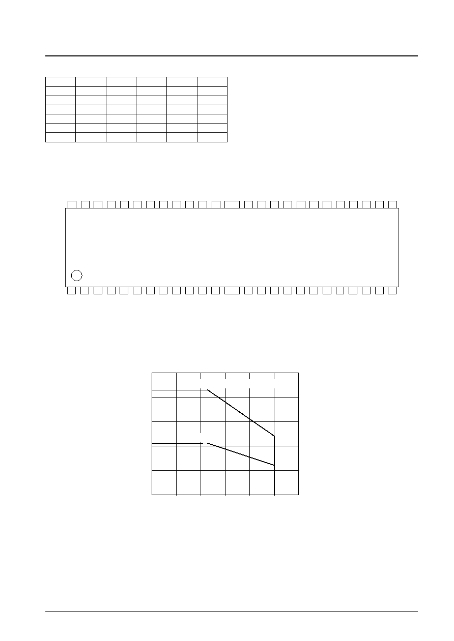
Pin Arrangement
Pdmax -- Ta Characteristics Curve
LB11870
47
VREG
NC
46
NC
OUT3
44
43
42
41
40
39
48
36
35
34
33
31
30
29
28
27
NC
NC
NC
VCC2
S/S
CLK
BRSEL
PH
FGS
LD
NC
NC
CLD
13
14
15
16
17
18
19
20
21
PD
FRAME
NC
EI
GND1
FGIN≠
PWM
GND2
FGIN+
FRAME
9
8
7
6
5
4
3
2
1
IN3≠
NC
IN2≠
IN2+
OUT1
NC
IN3+
NC
OUT2
10
38
22
37
VCC1
NC
FC
NC
GND3
NC
11
12
23
24
26
25
32
45
VM1
VM2
CSD
FGFIL
EO
TOC
IN1≠
IN1+
2.0
0.8
1.6
1.2
0.4
100
80
60
40
20
0
≠20
0.85W
0.476W
0.963W
1.72W
Mounted on a board (114.3
◊
76.1
◊
1.6mm, glass epoxy)
Pd max -- Ta
Ambient temperature, Ta --
∞
C
Power dissipation, Pd max -- W
Independent IC
No. 7256 -5/14
LB11870
Pin Functions
Pin
Pin No.
OUT1
OUT2
OUT3
3
1
46
Outputs
The PWM signal controls the duty from the low side transistor.
IN1+, IN1≠
IN2+, IN2≠
IN3+, IN3≠
11, 12
9, 10
6, 8
Hall inputs for the three phases
The logic H state means that V
IN
+ is greater than V
IN
≠.
FG IN+
13
FG comparator noninverting input
FG IN≠
14
FG comparator inverting input
GND1
15
Control system ground
GND2
16
Subsidiary ground.
PWM
17
Sets the PWM oscillator frequency. Insert a capacitor between this pin and ground.
FC
19
Current control circuit frequency characteristics correction. Insert a capacitor between this pin and ground.
PD
21
Phase comparator output. Outputs the phase error as changes in the pulse duty.
EI
22
Error amplifier input
EO
23
Error amplifier output
TOC
24
Torque command input. This pin is normally connected to the EO pin. When the TOC potential falls, the low side output
transistor on duty is changed and the torque increases.
FGFIL
25
FG filter connection. Insert a capacitor between this pin and ground if noise on the FG signal is a problem.
CSD
26
Sets the operating time for the rotor constraint protection circuit and the initial reset operation.
Insert a capacitor between this pin and ground. If the rotor constraint protection circuit is not used, insert a resistor in
parallel with this capacitor.
CLD
27
Sets the phase locked signal mask time. Insert a capacitor between this pin and ground. Leave this pin open if there is no
need to mask.
FGS
28
FG Schmitt output. This is an open-collector output.
LD
29
Phase locked state detection output. This output goes to the on state when the PLL phase is locked. This is an open-
collector output.
S/S
32
Start/stop control input. Low: start, High or open: stop.
CLK
33
Clock input. The maximum input frequency is 10 kHz.
BRSEL
34
Deceleration control switching input. Low: Reverse torque control, High or open: free running.
An external Schottky barrier diode is required on the output low side if reverse torque control is used.
PH
35
Smoothes the RF waveform. Insert a capacitor between this pin and ground.
VREG
36
5 V regulator output (control circuit power supply). Insert a capacitor between this pin and ground for power supply
stabilization.
VM1
37
Output block power supply. Short this pin to VM2.
VM2
38
Output current detection. Insert a resistor between this pin and V
CC
1.
The maximum output current IOUT is set to be IOUT = 0.5/Rf.
V
CC
2
39
Upper diode cathode connection. Short this pin to V
CC
1.
V
CC
1
40
Power supply. Insert a capacitor between this pin and ground to assure that noise does not enter the IC.
GND3
44
Output circuit block ground.
FRAME
Connect this pin to ground. The FRAME pin is connected internally to the metal surface on the back of the package. To
improve thermal dissipation, solder this metal surface to the PCB.
NC
2, 4, 5, 7
18, 20, 30
31, 41, 42
43, 45, 47
48
Since these pins are not connected to the IC internally, they can be used for wiring connections.

Internal Equivalent Circuit Block Diagram and External Component Reference
No. 7256 -6/14
LB11870
≠
+
HALL LOGIC
HALL
HYS AMP
PWM
OSC
BRSEL
S/S
LOGIC
COMP
TSD
VREG
CLK
LD
PLL
FG
FILTER
≠
+
IN2+ IN2≠
IN3+
GND1
IN3≠
PWM
S/S
VREG
VM1
FGIN+
FGIN≠
LD
EO
EI
PD
TOC
VREG
VCC2
BRSEL
CSD
IN1+ IN1≠
CLK
DRIVER
OUT1
OUT2
OUT3
GND3
VREG
FGS
VCC
Rf
PEAK
HOLD
CURR
LIM
CONT
AMP
PH
FC
VREG
VREG
COUNT
CSD
OSC
GND2
LDMASK
CLD
FGFIL
VM2
VCC1
No. 7256 -7/14
LB11870
Pin Functions
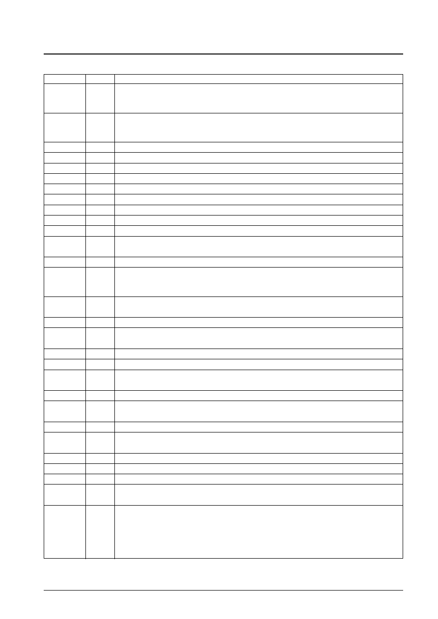
Pin No.
Pin
Function
Equivalent circuit
Motor drive output
3
1
46
OUT1
OUT2
OUT3
1
3
46
300
44
37
VCC1
38
39
VREG
8
300
11
9
6
12
10
300
Output block ground
44
GND3
Output block power supply and current detection.
Insert the resistor Rf between this pin and V
CC
1.
The output current will be limited to the current value
I
OUT
= VRF/Rf.
37
38
VM1
VM2
Upper diode cathode connection. Short this pin to V
CC
1.
39
V
CC
2
Hall element inputs.
The high state is when IN+ is greater than IN-, and the
low state is the reverse.
An amplitude of at least 100 mVp-p (differential) is
desirable for the Hall element signal inputs. If noise on
the Hall signals is a problem, insert capacitors between
the IN+ and IN≠ inputs.
11
12
9
10
6
8
IN1+
IN1≠
IN2+
IN2≠
IN3+
IN3≠
VREG
300
14
300
13
FG input.
If noise on the FG signal input is a problem, connect a
filter consisting of either a capacitor or a capacitor and a
resistor.
13
14
FGIN+
FGIN≠
Control circuit block ground
15
GND1
SUBGND pin
16
GND2
Continued on next page.
No. 7256 -8/14
LB11870
Continued from preceding page.
Pin No.
Pin
Function
Equivalent circuit
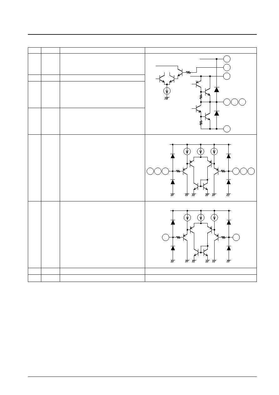
Sets the PWM oscillator frequency.
Insert a capacitor between this pin and ground.
The PWM oscillator frequency is set to about 34 kHz
when a 680 pF capacitor is used.
17
PWM
VREG
2k
200
17
Frequency characteristics correction for the current
control circuit.
Insert a capacitor (about 0.01 to 0.1 µF) between this pin
and ground.
The output duty is determined by comparing the voltage
on this pin to the PWM oscillator waveform.
19
FC
VREG
300
19
Phase comparator output
The phase error is converted to a pulse duty and output
from this pin.
21
PD
21
VREG
300
Error amplifier input
22
EI
VREG
300
22
Error amplifier output
23
EO
VREG
23
40k
Continued on next page.
No. 7256 -9/14
LB11870
Continued from preceding page.
Pin No.
Pin
Function
Equivalent circuit
Torque command voltage input.
This pin is normally connected to the EO pin. When the
TOC voltage falls, the lower output transistor on duty is
increased.
24
TOC
VREG
300
24
FG filter connection.
If noise on the FG signal input is a problem, insert a
capacitor (up to about 2200 pF) between this pin and
ground.
25
FGFIL
25
VREG
Sets the rotor constraint protection circuit operating time
and the initial reset pulse.
A protection operating time of about 8 seconds can be
set by insert a capacitor of about 0.068 µF between this
pin and ground. If the rotor constraint protection circuit is
not used, insert a resistor and a capacitor in parallel
between this pin and ground. (Values: about 220 k
and
4700 pF)
26
CSD
VREG
300
26
Sets the phase lock state signal mask time.
A mask time of about 90 ms can be set by inserting a
capacitor of about 0.1 µF between this pin and ground.
Leave this pin open if masking is not required.
27
CLD
VREG
27
300
FG Schmitt output
28
FGS
VREG
28
Continued on next page.
No. 7256 -10/14
LB11870
Continued from preceding page.
Pin No.
Pin
Function
Equivalent circuit
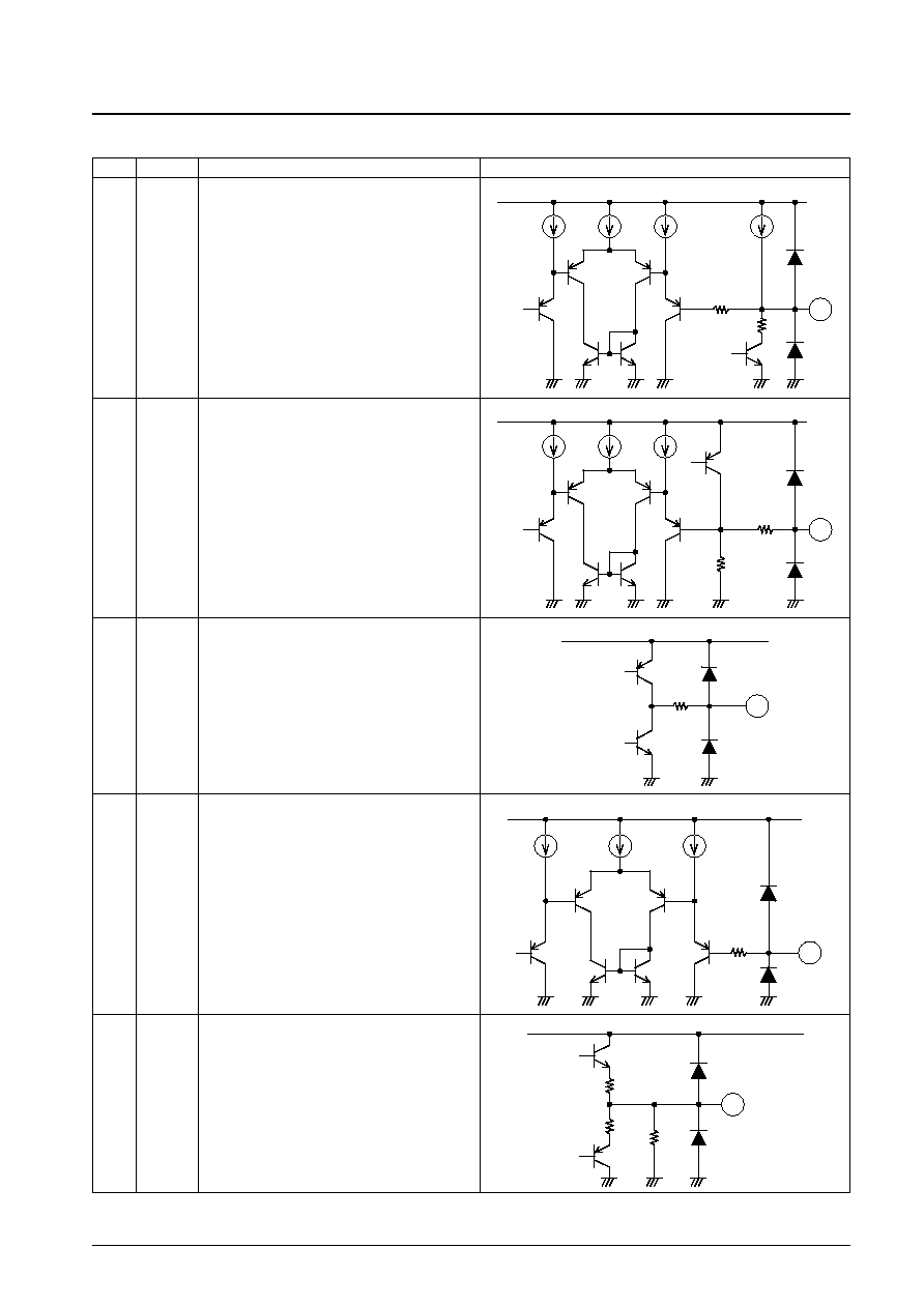
Phase lock state detection output.
This output goes to the on state (low level) when the
phase is locked.
29
LD
VREG
29
Start/stop control input
Low: 0 to 1.5 V
High: 3.5 V to VREG
Hysteresis: 0.5 V
Low: start. This pin goes to the high level when open.
32
S/S
VREG
22k
2k
32
Clock input.
Low: 0 to 1.5 V
High: 3.5 V to VREG
Hysteresis: 0.5 V
f
CLK
= 10 kHz (maximum)
If noise is a problem, use a capacitor to remove that
noise at this input.
33
CLK
VREG
22k
2k
33
Deceleration switching control input.
Low: 0 to 1.5 V
High: 3.5 V to VREG
This pin goes to the high level when open.
Low: reverse torque control, High: free running. An
external Schottky barrier diode is required on the output
low side if reverse torque control is used.
34
BRSEL
VREG
30k
2k
34
RF waveform smoothing.
If noise on the RF waveform is a problem, insert a
capacitor between this pin and ground.
35
PH
VREG
500
35
Continued on next page.
No. 7256 -11/14
LB11870
Continued from preceding page.
Pin No.
Pin
Function
Equivalent circuit
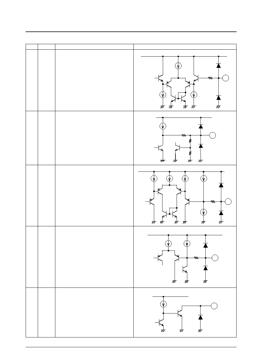
Stabilized power supply output (5 V output).
Insert a capacitor of about 0.1 µF between this pin and
ground for stabilization.
36
VREG
36
Vcc
Power supply.
Insert a capacitor of at least 10 µF between this pin and
ground to prevent noise from entering the IC.
40
V
CC
1
Since these pins are not connected to the IC internally,
they can be used for wiring connections.
2, 4, 5
7, 18
20, 30
31, 41
42, 43
45, 47
48
NC
Connect this pin to ground.
FRAME

Overview of the LB11870
1. Speed Control Circuit
This IC adopts a PLL speed control technique and provides stable motor operation with high precision and low jitter.
This PLL circuit compares the phase error at the edges of the CLK signal (falling edges) and FG signal (falling edges
on the FGIN+ and FGS signals), and the IC uses the detected error to control motor speed.
During this control operation, the FG servo frequency will be the same as the CLK frequency.
f
FG
(servo) = f
CLK
2. Output Drive Circuit
To minimize power loss in the output circuits, this IC adopts a direct PWM drive technique. The output transistors are
always saturated when on, and the IC adjusts the motor drive output by changing the output on duty. The low side
output transistor is used for the output PWM switching.
Both the high and low side output diodes are integrated in the IC. However, if reverse torque control mode is selected
for use during deceleration, or if a large output current is used and problems occur (such as incorrect operation or
waveform disruption due to low side kickback), a Schottky diode should be inserted between OUT and ground. Also,
if it is necessary to reduce IC heating during steady-state (constant speed) operation, it may be effective to insert a
Schottky diode between V
CC
and OUT. (This is effective because the load associated with the regenerative current
during PWM switching is born not by the on-chip diode but by the external diode.)
3. Current Limiter Circuit
The current limiter circuit limits the peak level of the current to a level determined by I = VRF/Rf (where VRF =
0.5 V (typical) and Rf is the value of the current detection resistor). The current limiter operates by reducing the
output on duty to suppress the current.
The current limiter circuit detects the reverse recovery current of the diode due to PWM operation. To assure that the
current limiting function does not malfunction, its operation has a delay of about 2 µs. If the motor coils have a low
resistance or a low inductance, current fluctuations at startup (when there is no reactive power in the motor) will be
rapid. The delay in this circuit means that at such times the current limiter circuit may operate at a point well above
the set current. Designers must take this increase in the current due to the delay into account when setting the current
limiter value.
4. Power Saving Circuit
This IC goes into a power saving state that reduces the current drain in the stop state. The power saving state is
implemented by removing the bias current from most of the circuits in the IC. However, the 5 V regulator output is
provided in the power saving state.
5. Reference Clock
Care must be taken to assure that no chattering or other noise is present on the externally input clock signal. Although
the input circuit does have hysteresis, if problems do occur, the noise must be excluded with a capacitor.
If the IC is set to the start state when the reference clock signal is not present, if the rotor constraint protection circuit
is used, the motor will turn somewhat and then motor drive will be shut off. However, if the rotor constraint
protection circuit is not used, and furthermore reverse torque control mode is selected for deceleration, the motor will
be driven at ever increasing speed in the reverse direction. (This is because the rotor constraint protection circuit
oscillator signal is used for clock cutoff protection.) Applications must implement a workaround for this problem if
there is any possibility whatsoever for it to occur.
6. Notes on the PWM Frequency
The PWM frequency is determined by the value of the capacitor C (in F) connected to the PWM pin.
f
PWM
.
=. 1 / (43000
◊
C)
If a 680 pF capacitor is used, the circuit will oscillate at about 34 kHz. If the PWM frequency is too low, the motor
will emit switching noise, and if it is too high, the power loss in the output will be excessive. A PWM frequency in
the range 15 to 50 kHz is desirable. To minimize the influence of the output on this circuit, the ground lead of this
capacitor should be connected as close as possible to the IC control system ground (the GND1 pin).
No. 7256 -12/14
LB11870

7. Hall Input Signals
Signals with an amplitude in excess of the hysteresis (42 mV maximum) must be provided as the Hall input signals.
However, an amplitude of over 100 mV is desirable to minimize the influence of noise. If the output waveforms are
disturbed (at phase switching) due to noise on the Hall inputs, insert capacitors across these inputs.
8. FG Input Signal
Normally, one phase of the Hall signals is input as the FG signal. If noise is a problem the input must be filtered with
either a capacitor or an RC filter circuit. Although it is also possible to remove FG signal noise by inserting a
capacitor between the FGFIL pin and ground, the IC may not be able to operate correctly if this signal is damped
excessively. If this capacitor is used, its value must be less than about 2200 pF. If the location of this capacitor's
ground lead is inappropriate, it may, inversely, make noise problems even more likely to occur. Thus the ground lead
location must be chosen carefully.
9. Rotor Constraint Protection Circuit
This IC provides a rotor constraint protection circuit to protect the IC itself and the motor when the motor is
constrained. If the LD output is high (unlocked) for over a certain fixed period with the IC in the start state, the low
side transistor will be turned off. The time constant is determined by the capacitor connected to the CSD pin.
<time constant (in seconds)>
.
=. 120
◊
C (µF)
If a 0.068 µF capacitor is used, the protection time will be about 8 seconds. The set time must be selected to have an
adequate margin with respect to the motor startup time. This protection circuit will not operate during deceleration
when the clock frequency is switched. To clear the rotor constraint protection state, the IC must be set to the stopped
state or the power must be turned off and reapplied.
Since the CSD pin also functions as the initial reset pulse generation pin at startup, the logic circuit will go to the
reset state and the IC will not be able to function if this pin is connected to ground. Therefore, both a 220 k
resistor
and a 4700 pF capacitor must be inserted between this pin and ground if the rotor constraint protection circuit is not
used.
10. Phase Lock Signal
(1) Phase lock range
Since this IC does not include a counter or similar functionality in the speed control system, the speed error range
in the phase locked state cannot be determined solely by IC characteristics. (This is because the acceleration of the
changes in the FG frequency influences the range.) When it is necessary to stipulate this characteristic for the
motor, the designer must determine this by measuring the actual motor state. Since speed errors occur easily in
states where the FG acceleration is large, it is thought that the speed errors will be the largest during lock pull-in at
startup and when unlocked due to switching clock frequencies.
(2) Masking function for the phase lock state signal
A stable lock signal can be provided by masking the short-term low-level signals due to hunting during lock pull-
in. However, this results in the lock state signal output being delayed by the masking time.
The masking time is determined by the capacitor inserted between the CLD pin and ground.
<masking time (seconds)>
.
=. 0.9
◊
C (µF)
When a 0.1 µF capacitor is used, the masking time will be about 90 ms. In cases where complete masking is required,
a masking time with fully adequate margin must be used. If no masking is required, leave the CLD pin open.
No. 7256 -13/14
LB11870
PS No. 7256 -14/14
LB11870
11. Power Supply Stabilization
Since this IC provides a large output current and adopts a switching drive technique, the power supply line level can
be disrupted easily. Thus capacitors large enough to stabilize the power supply voltage must be inserted between the
VCC pins and ground. The ground leads of these capacitors must be connected to the three pins that are the power
grounds, and they must be connected as close as possible to the pins themselves. If these capacitors (electrolytic
capacitors) cannot be connected close to their corresponding pins, ceramic capacitors of about 0.1 µF must be
connected near these pins.
If reverse torque control mode is selected for use during deceleration, since there are states where power is returned to
the power supply system, the power supply line levels will be particularly easily disrupted. Since the power line level
is most easily disrupted during lock pull-in at high motor speeds, this state needs extra attention; in particular,
capacitors that are adequately large to handle this situation must be selected.
If diodes are inserted in the power supply lines to prevent destruction of the device if the power supply is connected
with reverse polarity, the power supply line levels will be even more easily disrupted, and even larger capacitors must
be used.
12. VREG Stabilization
A capacitor of at least 0.1 µF must be used to stabilize the VREG voltage, which is the control circuit power supply.
The ground lead of that capacitor must be connected as close as possible to the IC control system ground (GND1).
13. Error Amplifier External Component Values
To prevent adverse influence from noise, the error amplifier external components must be located as close to the IC
as possible. In particular, they must be located as far from the motor as possible.
14. FRAME Pin and the IC Metallic Rear Surface
The FRAME pin must be connected to the GND1 and GND2 pins, and the ground side of the electrolytic capacitor
must be connected to GND3. The IC's metallic rear surface is connected to the FRAME pin internally to the IC.
Thermal dissipation can be improved significantly by tightly bonding the metallic surface of the back of the IC
package to the PCB with, for example, a solder with good thermal conductivity.
This catalog provides information as of August, 2002. Specifications and information herein are subject to
change without notice.
Specifications of any and all SANYO products described or contained herein stipulate the performance,
characteristics, and functions of the described products in the independent state, and are not guarantees
of the performance, characteristics, and functions of the described products as mounted in the customer's
products or equipment. To verify symptoms and states that cannot be evaluated in an independent device,
the customer should always evaluate and test devices mounted in the customer's products or equipment.
SANYO Electric Co., Ltd. strives to supply high-quality high-reliability products. However, any and all
semiconductor products fail with some probability. It is possible that these probabilistic failures could
give rise to accidents or events that could endanger human lives, that could give rise to smoke or fire,
or that could cause damage to other property. When designing equipment, adopt safety measures so
that these kinds of accidents or events cannot occur. Such measures include but are not limited to protective
circuits and error prevention circuits for safe design, redundant design, and structural design.
In the event that any or all SANYO products (including technical data, services) described or contained
herein are controlled under any of applicable local export control laws and regulations, such products must
not be exported without obtaining the export license from the authorities concerned in accordance with the
above law.
No part of this publication may be reproduced or transmitted in any form or by any means, electronic or
mechanical, including photocopying and recording, or any information storage or retrieval system,
or otherwise, without the prior written permission of SANYO Electric Co., Ltd.
Any and all information described or contained herein are subject to change without notice due to
product/technology improvement, etc. When designing equipment, refer to the "Delivery Specification"
for the SANYO product that you intend to use.
Information (including circuit diagrams and circuit parameters) herein is for example only; it is not
guaranteed for volume production. SANYO believes information herein is accurate and reliable, but
no guarantees are made or implied regarding its use or any infringements of intellectual property rights
or other rights of third parties.