 | –≠–ª–µ–∫—Ç—Ä–æ–Ω–Ω—ã–π –∫–æ–º–ø–æ–Ω–µ–Ω—Ç: LB11880 | –°–∫–∞—á–∞—Ç—å:  PDF PDF  ZIP ZIP |
Ordering number : ENN6470
52600RM (OT) No. 6470-1/9
Overview
The LB11880 is a sensorless motor driver that also
includes a loading motor driver. It is ideal for drum motor
drive in VCR products.
Functions and Features
∑ Soft switching drive
∑ No Hall sensors required
∑ No FG sensors required
∑ Built-in PG amplifier
∑ Built-in thermal shutdown circuit
∑ Current limiter circuit
∑ On-chip loading motor driver
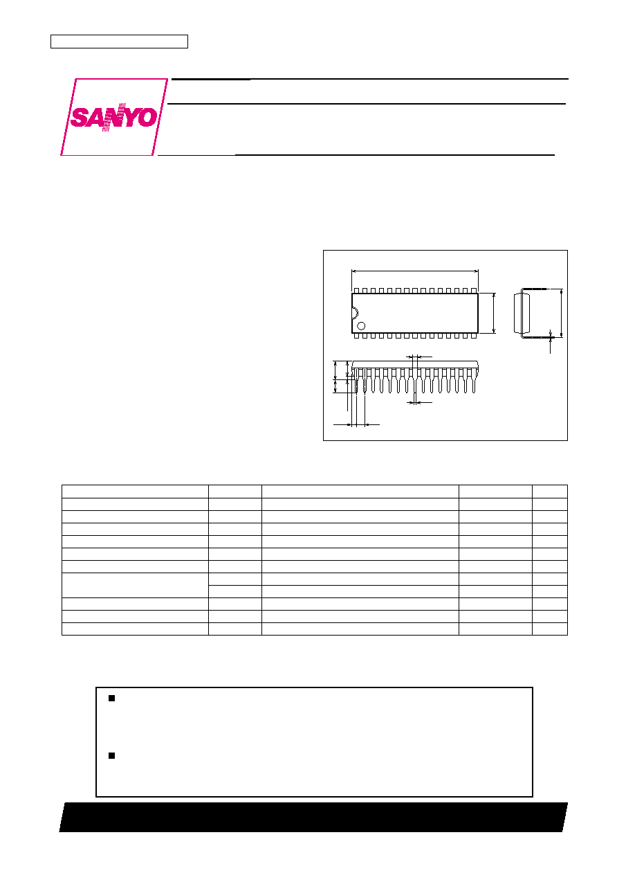
Package Dimensions
unit: mm
3196A-DIP30SD
(1.04)
1.78
0.95
0.48
10.16
3.95mas
(3.25)
0.51min
3.0
0.25
1
15
30
16
8.6
27.0
SANYO: DIP30SD
[LB11880]
LB11880
SANYO Electric Co.,Ltd. Semiconductor Company
TOKYO OFFICE Tokyo Bldg., 1-10, 1 Chome, Ueno, Taito-ku, TOKYO, 110-8534 JAPAN
Three-Phase Sensorless Motor Driver with
Loading Motor Driver
Monolithic Digital IC
Any and all SANYO products described or contained herein do not have specifications that can handle
applications that require extremely high levels of reliability, such as life-support systems, aircraft's
control systems, or other applications whose failure can be reasonably expected to result in serious
physical and/or material damage. Consult with your SANYO representative nearest you before using
any SANYO products described or contained herein in such applications.
SANYO assumes no responsibility for equipment failures that result from using products at values that
exceed, even momentarily, rated values (such as maximum ratings, operating condition ranges, or other
parameters) listed in products specifications of any and all SANYO products described or contained
herein.
Parameter
Symbol
Conditions
Ratings
Unit
Maximum supply voltage 1
V
CC
max
14.5
V
Maximum supply voltage 2
V
CC
L max
14.5
V
Maximum supply voltage 3
VREG max
7.0
V
Output voltage
Vomax
14.5
V
Input voltage
VI1max
≠0.3 to VREG + 0.3
V
Cylinder current
Iomax
1.0
A
Loading current
Iomax (AVE)
0.4
A
Iomax (peak)
1.2
A
Allowable power dissipation
Pdmax
When mounted on the specified printed circuit board
*
2.8
W
Operating temperature
Topr
≠20 to +75
∞C
Storage temperature
Tstg
≠55 to +150
∞C
Specifications
Absolute Maximum Ratings
at Ta = 25∞C
Note:
*
Specified printed circuit board: 114.3
◊
76.1
◊
1.6 mm glass-epoxy board
No. 6470-2/9
LB11880
Parameter
Symbol
Conditions
Ratings
Unit
Supply voltage 1
V
CC
8 to 13.8
V
Supply voltage 2
V
CC
L
8 to 13.8
V
Supply voltage 3
VREG
4 to 6
V
Allowable Operating Ranges
at Ta = 25∞C
Parameter
Symbol
Conditions
Ratings
Unit
min
typ
max
Supply current 1
I
CC
VC = 0 V, XIN = YIN = 0 V
3.5
5.0
mA
Supply current 2
I
CC
L
VC = 0 V, XIN = YIN = 0 V
1
mA
Supply current 3
I
REG
VC = 0 V, XIN = YIN = 0 V
10
15
mA
Output saturation voltage 1
V
O
sat1
IO = 0.4 A, source + sink
1.4
2.0
V
Output saturation voltage 2
V
O
sat2
IO = 0.8 A, source + sink
1.8
2.6
V
MC pin common-mode input voltage range
V
IC
0
V
CC
≠ 2
V
VC pin input bias current
I
VC
VC = 0 V
≠2
≠1
µA
Control start voltage
VTHVC
VRF = 10 mA
2.4
2.5
2.6
V
Closed-loop control gain
GMVC
RF = 0.5
0.75
0.95
1.15
A/V
PCOUT output current 1
I
PCO
U
Source side
≠90
µA
PCOUT output current 2
I
PCO
D
Sink side
90
µA
VCOIN input current
I
VCO
IN
VCOIN = 5 V
0.1
0.2
µA
Minimum VCO frequency
f
VCO
MIN
CX = 0.022 µF, V
CO
IN = open
400
Hz
Maximum VCO frequency
f
VCO
MAX
CX = 0.022 µF, V
CO
IN = 5 V
18.5
kHz
C1/C2 source current ratio
R
SOURCE
I
C1SOURCE
/I
C2SOURCE
≠12
+12
%
C1/C2 sink current ratio
R
SINK
I
C1SINK
/I
C2SINK
≠12
+12
%
C1 source/sink current ratio
RC1
I
C1SOURCE
/I
C1SINK
≠35
+15
%
C2 source/sink current ratio
RC2
I
C2SOURCE
/I
C2SINK
≠35
+15
%
Thermal shutdown operating temperature
T-TSD
*
150
180
210
∞C
Thermal shutdown hysteresis
TTSD
*
15
∞C
Electrical Characteristics
at Ta = 25∞C, V
CC
= V
CC
L = 12 V, VREG = 5 V
Parameter
Symbol
Conditions
Ratings
Unit
min
typ
max
[Back EMF FG]
Output on voltage
V
O
L
0.4
V
Output off voltage
V
O
H
4.5
V
[PG Amplifier]
Input offset voltage
V
I
O
≠8
+8
mV
Input bias current
I
B
IN≠
≠250
nA
Common-mode input voltage range
V
ICOM
*
1
3.5
V
Open-loop gain
GVPG
f = 1 kHz
55
dB
Output on voltage
V
O
L
0.4
V
Output off voltage
V
O
H
4.5
V
Schmitt amplifier hysteresis
V
S
hys
70
93
115
mV
FG/PG Amplifier Block
at Ta = 25∞C, V
CC
= V
CC
L = 12 V, VREG = 5 V
Note:
*
These values are design guarantee values, and are not tested.
Note:
*
These values are design guarantee values, and are not tested.
No. 6470-3/9
LB11880
Parameter
Symbol
Conditions
Ratings
Unit
min
typ
max
Input voltage
1 (high)
V
IN
1
3.5
5
V
2 (low)
V
IN
2
0
0.8
V
Input current
I
IN
Sink V
IN
= 3.5 V
30
50
µA
Input hysteresis
VT
0.7
V
Vsat U-1
Vref = VS, between the output and VS
1.5
2.1
V
I
O
= 0.2 A, CW/CCW mode
Vsat L-1
Vref = VS, between the output and ground
0.2
0.3
V
Saturation voltage
I
O
= 0.2 A, CW/CCW mode
Vsat U-1'
Vref = VS, between the output and VS
1.6
2.2
V
I
O
= 0.4 A, CW/CCW mode
Vsat L-1'
Vref = VS, between the output and ground
0.3
0.5
V
I
O
= 0.4 A, CW/CCW mode
VsatU-1''
Vref = 8 V, between the output and ground
7.2
8.0
8.8
V
Upper side residual voltage
I
O
= 0.2 A, CW/CCW mode
VsatL-1''
Vref = 8 V, between the output and ground
7.2
8.0
8.8
V
I
O
= 0.4 A, CW/CCW mode
Output transistor leakage current
Upper
ILU
50
µA
Lower
ILL
50
µA
Diode forward voltage
Uper
VFU
IF = 0.4 A
1.3
V
Lower
VFL
IF = 0.4 A
1.0
V
Control supply current
Iref
≠5
≠2
µA
Loading Block
at Ta = 25∞C, V
CC
= V
CC
L = 12 V, VREG = 5 V
No. 6470-4/9
LB11880
Loading Motor Truth Table
Input
Output
Mode
X
IN
Y
IN
X
OUT
Y
OUT
L
L
Off
Off
Standby
H
L
H
L
Forward
L
H
L
H
Reverse
H
H
L
L
Brake
0
1
2
3
4
≠20
0
20
40
60
80
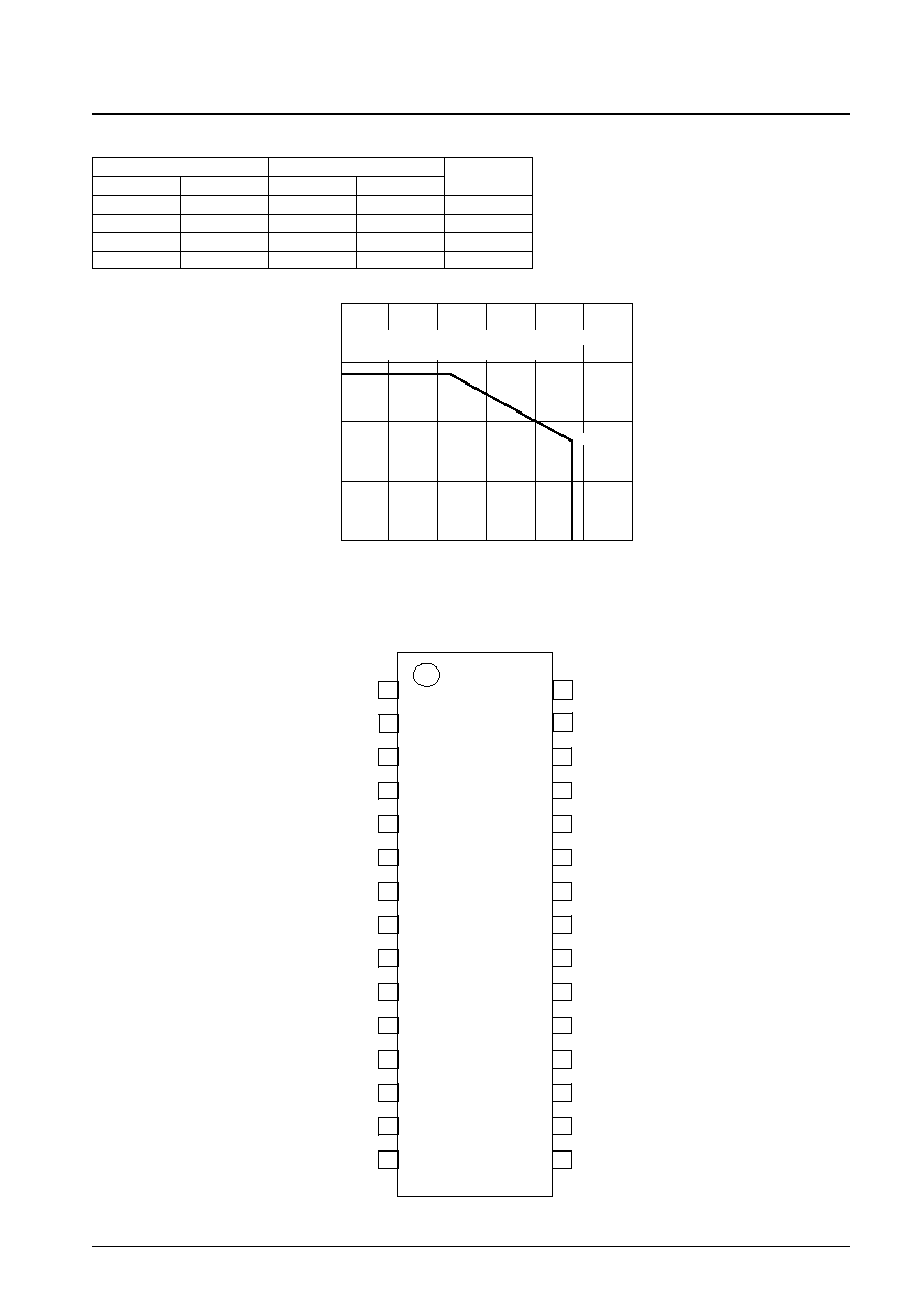
100
Allowable power dissipation, Pdmax -- W
Pd max -- Ta
Ambient temperature, Ta --
∞
C
When mounted on the specified printed circuit board
(114.3
◊
76.1
◊
1.6 mm
3
glass-epoxy board)
1.68
2.80
13
14
12
11
10
9
8
7
6
5
4
3
2
1
29
15
16
17
18
19
20
21
22
23
24
25
26
27
30
28
LB11880
W
OUT
U
IN
MCOM
RF
GND
VREG
W
IN
C1
CX
C2
VCO
IN
PC
OUT
Y
OUT
LGND
X
OUT
X
IN
LV
CC
VREF
V
IN
BFGO
PG
OUT
1
PG
OUT
2
PG
IN
+
PG
IN
≠
VC
FC
V
CC
V
OUT
U
OUT
Top view
Y
IN
Pin Assignment
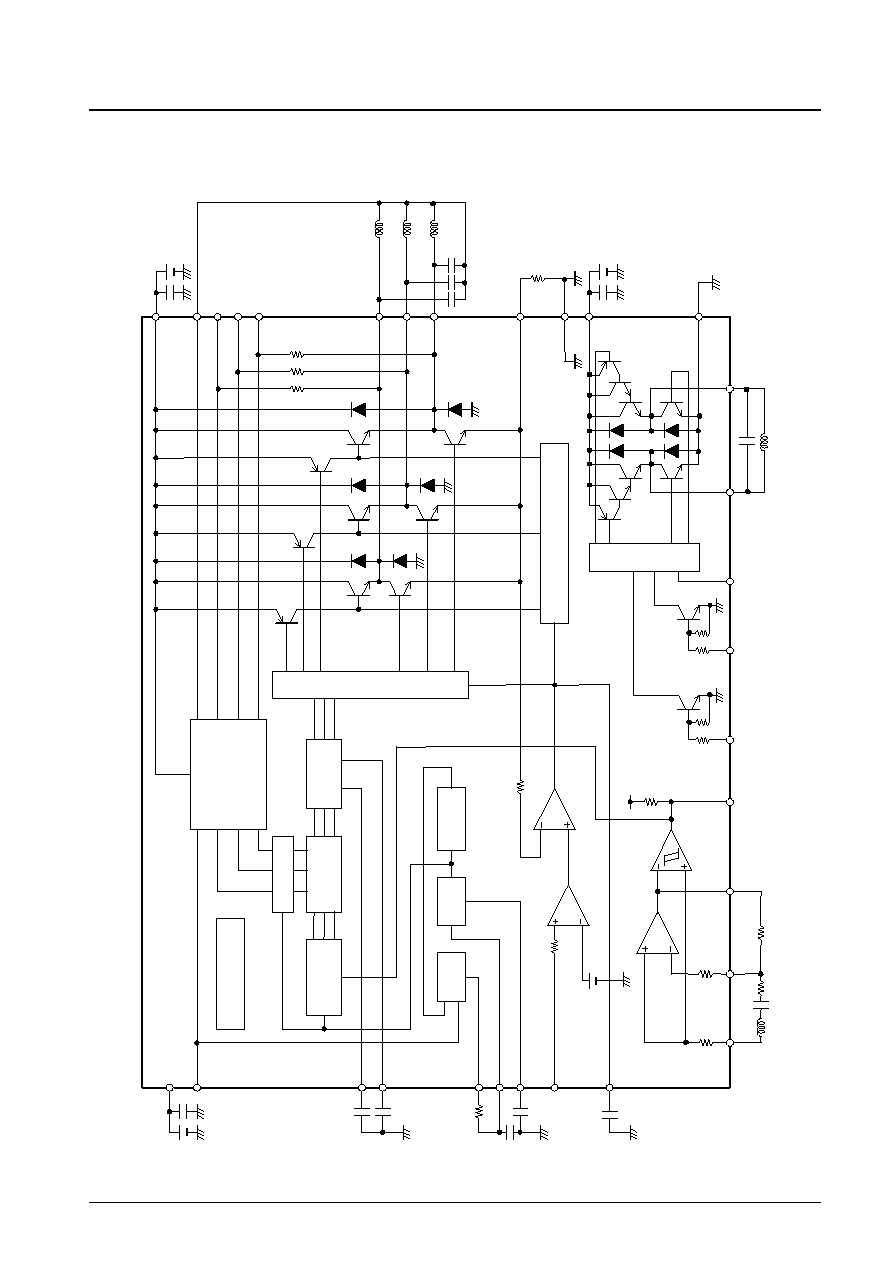
Block Diagram
(Note that the values of the external components depend on the motor used.)
No. 6470-5/9
LB11880
Soft switching
drive circuit
VCO
PLL
Divide-by-
8 circuit
Thermal shutdown
circuit
Upper side saturation
prevention circuit
Mask circuit
Timing control
circuit
Startup control
circuit
Rotor position
detection circuit
Output drive circuit
V
CC
MC
OM
U
OUT
V
OUT
W
OUT
RF
0.5
GND
CX
VCO
IN
PC
OUT
PG
IN
+
V
REG
1 k
200
0.1
µ
F
VC
FC
C2
C1
BFG
O
VREG
PG
OUT
1P
G
OUT
2
5 k
PG
IN
-
200
200
X
IN
Y
IN
LGND
Output drive circuit
Y
OUT
X
OUT
LV
CC
VREF
U
IN
V
IN
W
IN
560 k
0.47
µ
F
0.022
µ
F
2200 pF
2200 pF
0.022
µ
F
◊
3
6
30
µ
A
60
µ
A
38
38
5 k
V
REG
4
5 k
1 k
10 k
5 k
1
V
REG
6
µ
A
6
µ
A
6
µ
A
V
REG
5
200
200
4
10 k
10 k
No. 6470-6/9
LB11880
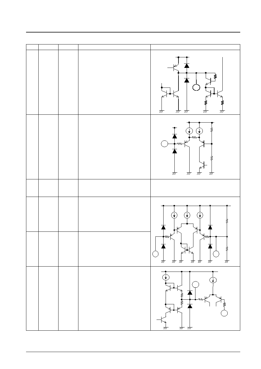
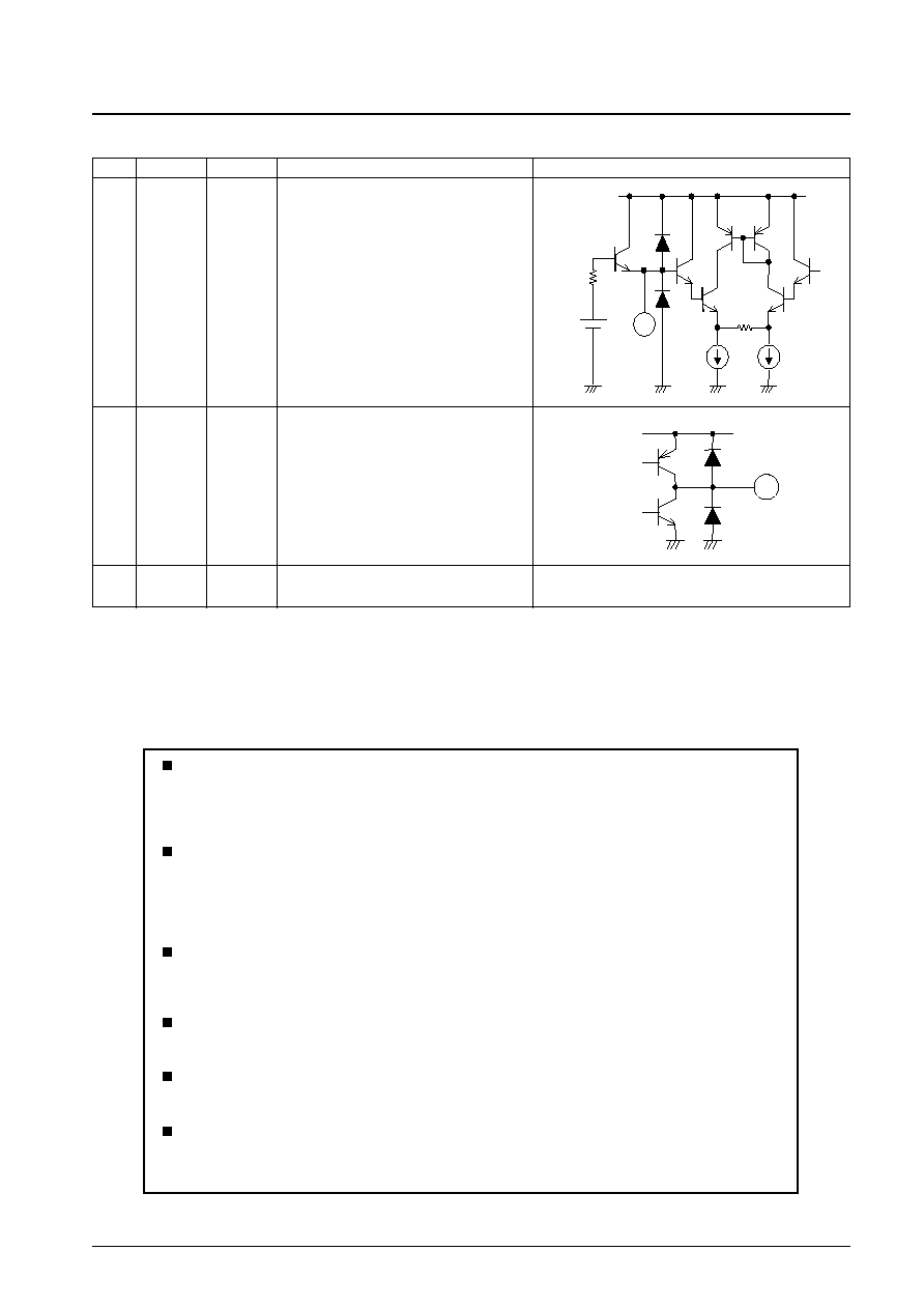
Pin Description
Pin No.
Pin
Pin voltage
Function
Equivalent circuit
Frequency characteristics compensation
Oscillation in the current control system closed
loop can be prevented by connecting a capacitor
between this pin and ground.
1
FC
Speed control
This circuit implements constant-current control in
which current feedback is applied from the RF
system.
2
VC
0 V to VREG
Control system power supply
This power supply must be stabilized so that ripple
and noise do not enter the IC.
3
VREG
4 V to 6 V
PG amplifier plus side input
This pin is biased to 1/2 VREG internally.
4
PG
IN
+
PG amplifier minus side input
5
PG
IN
≠
PG amplifier linear output
6
PG
OUT
1
Continued on next page.
40 k
27 k
24 k
V
CC
V
REG
50
µ
A
50
µ
A
2
200
2 k
2 k
13
15
9
14
10
11
100 k
50 k
V REG
50 k
12
10
1 mA
30 k
VCCL
50 k
1 mA
30 k
13 15
7
100
µ
A
5 k
VREG
8
VCC
VREG+VF
No. 6470-7/9
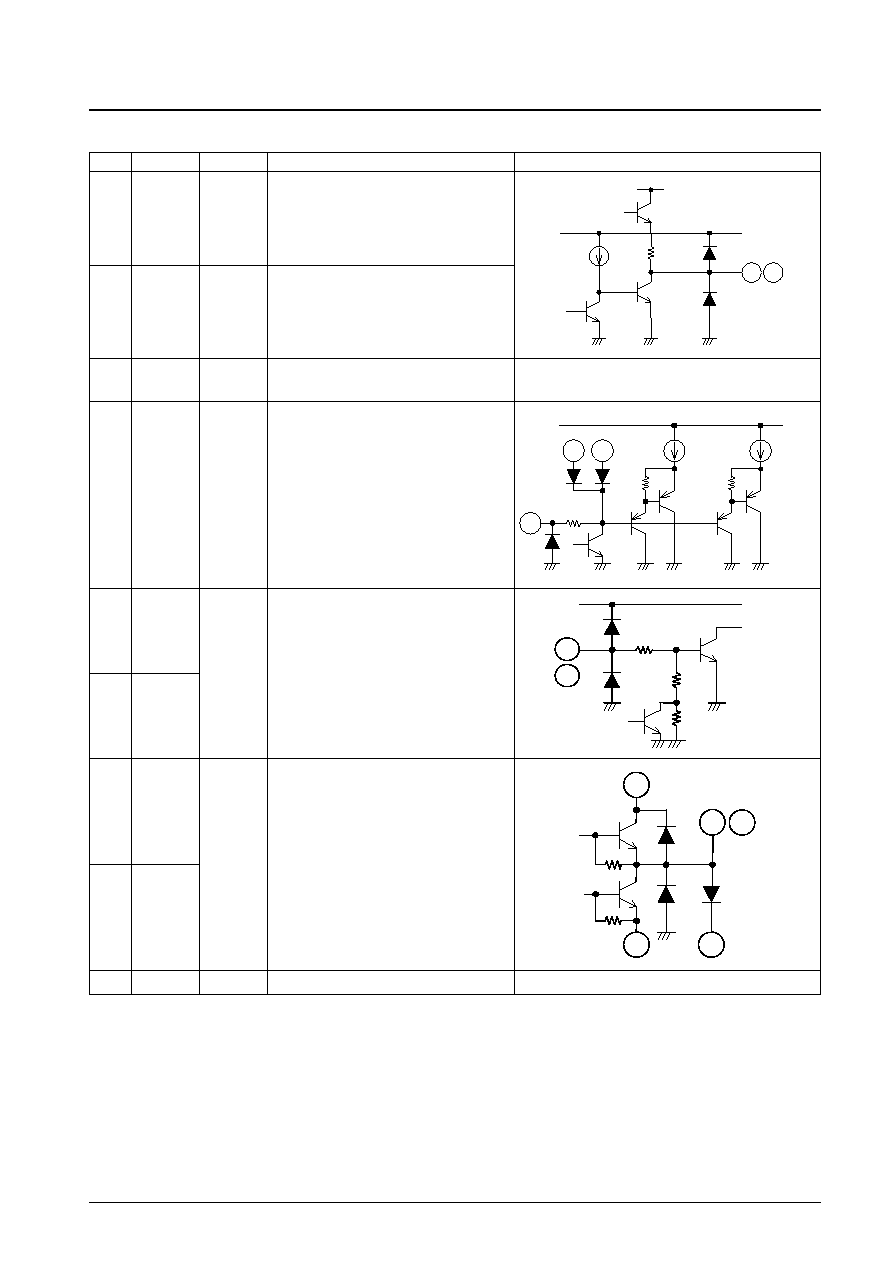
LB11880
Continued from preceding page.
Pin No.
Pin
Pin voltage
Function
Equivalent circuit
PG Schmitt amplifier output
7
PG
OUT
2
Motor back EMF voltage detection FG output
(synthesized from three phases)
8
BFGO
Loading motor driver output transistor power
supply
9
LV
CC
8 to 13.8 V
Loading motor driver output voltage setting
10
VREF
0 to V
CC
L
Loading motor driver logic input
11
X
IN
0 V to VREG
12
Y
IN
Loading motor driver output
Loading motor driver output transistor ground
13
X
OUT
15
Y
OUT
14
LGND
Continued on next page.
No. 6470-8/9
LB11880
Continued from preceding page.
Pin No.
Pin
Pin voltage
Function
Equivalent circuit
Drum motor driver output
Lowest potential of the drum motor driver output
transistor
This IC implements constant-current control by
detecting this voltage.
The current limiter also operates by detecting this
voltage.
16
U
OUT
20
µ
A
3.9
3.9
V
CC
16
18
17
22
20
23
24
30 k
30 k
10 k
VCC
200
23
24
22
19
200
200
2 k
16 17 18
10 k
17
V
OUT
18
W
OUT
20
RF
Internal reference voltage and power supply for
both the drum motor driver output block and the
coil waveform detection circuit.
21
V
CC
8 to 13.8 V
Motor coil center input
The coil voltage waveform is detected with this
voltage as the reference.
19
MCOM
1/2VREG
-VF
1 k
V
REG
5
µ
A
15
µ
A
15
µ
A
26
25
100
µ
A
300
V
REG
27
Triangular wave generating capacitor connection
This triangular wave is used to implement soft
switching in the coil output waveform.
The value of the capacitor connected between this
pin and ground determines the operating frequency
range and the minimum operating frequency of the
VCO circuit.
25
C1
26
C2
27
CX
Coil waveform detection comparator input
Each phase output is connected by an internal
10 k
resistor.
22
U
IN
23
V
IN
24
W
IN
Continued on next page.
PS No. 6470-9/9
LB11880
This catalog provides information as of May, 2000. Specifications and information herein are subject to
change without notice.
Specifications of any and all SANYO products described or contained herein stipulate the performance,
characteristics, and functions of the described products in the independent state, and are not guarantees
of the performance, characteristics, and functions of the described products as mounted in the customer's
products or equipment. To verify symptoms and states that cannot be evaluated in an independent device,
the customer should always evaluate and test devices mounted in the customer's products or equipment.
SANYO Electric Co., Ltd. strives to supply high-quality high-reliability products. However, any and all
semiconductor products fail with some probability. It is possible that these probabilistic failures could
give rise to accidents or events that could endanger human lives, that could give rise to smoke or fire,
or that could cause damage to other property. When designing equipment, adopt safety measures so
that these kinds of accidents or events cannot occur. Such measures include but are not limited to protective
circuits and error prevention circuits for safe design, redundant design, and structural design.
In the event that any or all SANYO products (including technical data, services) described or contained
herein are controlled under any of applicable local export control laws and regulations, such products must
not be exported without obtaining the export license from the authorities concerned in accordance with the
above law.
No part of this publication may be reproduced or transmitted in any form or by any means, electronic or
mechanical, including photocopying and recording, or any information storage or retrieval system,
or otherwise, without the prior written permission of SANYO Electric Co., Ltd.
Any and all information described or contained herein are subject to change without notice due to
product/technology improvement, etc. When designing equipment, refer to the "Delivery Specification"
for the SANYO product that you intend to use.
Information (including circuit diagrams and circuit parameters) herein is for example only; it is not
guaranteed for volume production. SANYO believes information herein is accurate and reliable, but
no guarantees are made or implied regarding its use or any infringements of intellectual property rights
or other rights of third parties.
Continued from preceding page.
Pin No.
Pin
Pin voltage
Function
Equivalent circuit
VCO circuit voltage input
The PCOUT pin voltage is filtered by an RC circuit
and input to this pin.
28
VCO
IN
50
µ
A
50
µ
A
50 k
V
REG
10 k
1.75 V
28
VCO circuit PLL output
29
PC
OUT
29
V
REG
Ground for all circuits other than the drum and
loading driver output transistors.
30
GND