 | –≠–ª–µ–∫—Ç—Ä–æ–Ω–Ω—ã–π –∫–æ–º–ø–æ–Ω–µ–Ω—Ç: LB11987 | –°–∫–∞—á–∞—Ç—å:  PDF PDF  ZIP ZIP |
Ordering number :ENN
*
6212A
70999RM (OT) No. 6212-1/6
Functions
∑ Three-phase full-wave current linear drive
∑ Built-in current limiter circuit
∑ Built-in saturation prevention circuits in both the upper
and lower sides of the output stage.
∑ FG amplifier
∑ Thermal shutdown circuit
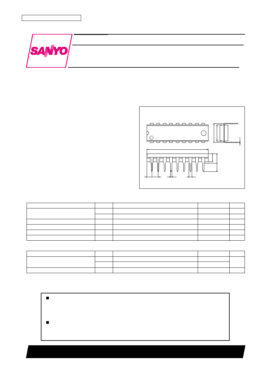
Package Dimensions
unit: mm
3007A-DIP18
1
9
18
10
24.2
1.94 2.54
1.2
0.5
3.25
3.3
3.85max
0.25
7.62
6.4
Preliminary
SANYO: DIP18
[LB11987]
SANYO Electric Co.,Ltd. Semiconductor Company
TOKYO OFFICE Tokyo Bldg., 1-10, 1 Chome, Ueno, Taito-ku, TOKYO, 110-8534 JAPAN
Monolithic Digital IC
LB11987
Refrigerator Fan Motor Driver
Any and all SANYO products described or contained herein do not have specifications that can handle
applications that require extremely high levels of reliability, such as life-support systems, aircraft's
control systems, or other applications whose failure can be reasonably expected to result in serious
physical and/or material damage. Consult with your SANYO representative nearest you before using
any SANYO products described or contained herein in such applications.
SANYO assumes no responsibility for equipment failures that result from using products at values that
exceed, even momentarily, rated values (such as maximum ratings, operating condition ranges, or other
parameters) listed in products specifications of any and all SANYO products described or contained
herein.
Parameter
Symbol
Conditions
Ratings
Unit
Maximum supply voltage
V
CC
max
24
V
V
S
max
24
V
Maximum output current
I
O max
1.3
A
Allowable power dissipation
Pdmax
Independent IC
1.13
W
Operating temperature
Topr
≠30 to +75
∞C
Storage temperature
Tstg
≠55 to +150
∞C
Specifications
Absolute Maximum Ratings
at Ta = 25∞C
Parameter
Symbol
Conditions
Ratings
Unit
Supply voltage
V
S
5 to 22
V
V
CC
7 to 22
Hall input amplitude
V
HALL
Between Hall inputs
±30 to ±80
mV 0-P
Allowable Operating Ranges
at Ta = 25∞C
No. 6212-2/6
LB11987
Electrical Characteristics
at Ta = 25∞C, V
CC
= 12 V, Vs = 12V
Parameter
Symbol
Conditions
Ratings
Unit
min
typ
max
V
CC
current drain
I
CC
R
L
= 560
(Y)
15
24
mA
[Output]
V
Osat
1
I
O
= 500 mA, Rf = 0.5
, Sink + Source
2.1
2.6
V
Output saturation voltage
(Saturation prevention function included)
V
Osat
2
I
O
= 1.0 A, Rf = 0.5
, Sink + Source
2.6
3.5
V
(Saturation prevention function included)
Output leakage current
I
Oleak
1.0
mA
[Hall Amplifier]
Input offset voltage
V
off
(HALL)
≠6
+6
mV
Input bias current
I
b
(HALL)
V
IN
, W
IN
1
3
µA
Common-mode input voltage
V
cm
(HALL)
3
V
CC
≠ 3
V
[Current Limiter]
LIM pin current limit level
I
LIM
Rf = 0.5
,
1
A
With the Hall input logic states fixed (U, V, W = high, high, low)
[Saturation]
Saturation prevention circuit
V
Osat
(DET)
R
L
= 560
(Y), Rf = 0.5
,
0.28
V
lower side voltage setting
The voltage between each output and the corresponding Rf.
[FG Amplifier]
Upper side output saturation voltage
V
satu
(SH)
11.8
V
Lower side output saturation voltage
V
satd
(SH)
0.3
V
Hysteresis
Vhys
23
mV
TSD operating temperature
T-TSD
Design target value
*
170
∞C
Note
*
: Items shown to be design target values in the conditions column are not measured.
No. 6212-3/6
LB11987
Truth Table and Control Functions
Source
sink
Hall input
U
V
W
1
W
V
H
H
L
2
W
U
H
L
L
3
V
U
H
L
H
4
V
W
L
L
H
5
U
W
L
H
H
6
U
V
L
H
L
Note: For the Hall inputs, the input high state is defined to be the state where the
(+) input is at least 0.01 V higher than the corresponding (≠) input, and
the input low state is defined to be the state where the (+) input is at least
0.01 V lower than the corresponding (≠) input.
Note: Since this drive technique is a 180∞ current application scheme, the
phases other than the sink and the source phases will not turn off.
Pin Functions
Pin No.
Pin
Function
5
GND
Ground for circuits other than the output transistors.
Note that the Rf pin will be at the lowest potential of the output transistors.
3
FG-OUT
This is the FG amplifier output pin. Internally, it is a resistive load. (Pull up)
6
FC
Corrects the frequency characteristics of the saturation prevention circuit loop.
7, 8
U
IN
+, U
IN
≠
U-phase Hall input. Logic high refers to the state where IN+ > IN≠.
9, 10
V
IN
+, V
IN
≠
V-phase Hall input. Logic high refers to the state where IN+ > IN≠.
11, 12
W
IN
+, W
IN
≠
W-phase Hall input. Logic high refers to the state where IN+ > IN≠.
13
V
CC
Power supply provided to all IC internal circuits other than the output block.
This voltage must be stabilized so that ripple and noise do not enter the IC.
14
V
S
Output block power supply
15
Rf
17
U
OUT
U-phase Hall output
18
V
OUT
V-phase Hall output (These pins include internal spark killer diodes.)
1
W
OUT
W-phase Hall output
Used for output current detection. The current limiter circuit operates using the resistor (Rf) connected between
this pin and ground.
Note that the lower side saturation prevention circuit operates according to the voltage that appears on this pin.
Since the over-saturation level is set by this voltage, the level of the lower side saturation prevention circuit may
be degraded in the large current region if the value of Rf is made extremely small.
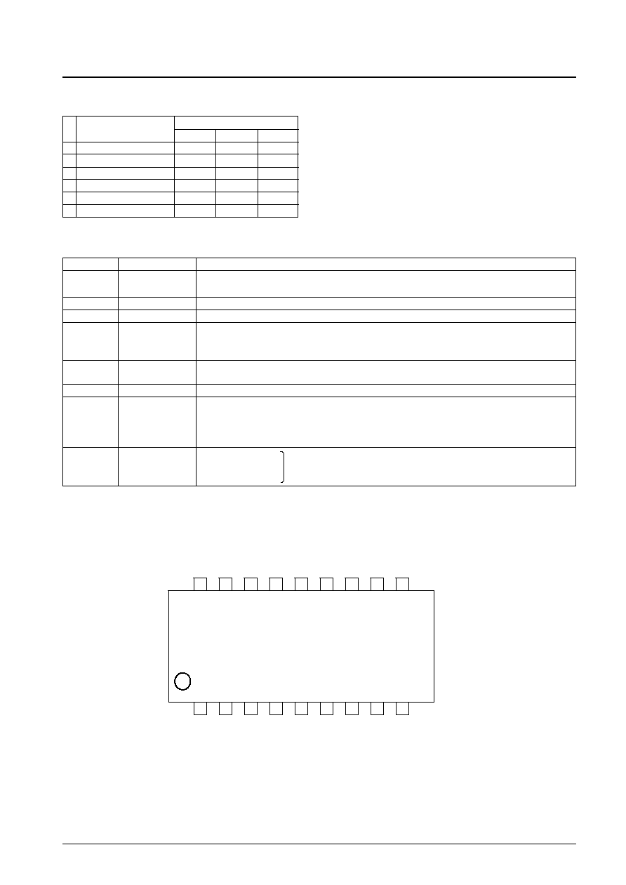
Pin Assignment
14
12
10
11
13
9
1
2
3
4
5
6
7
8
NC
WO
UT
LB11987
15
16
17
18
FGOUT
NC
GND
FC
UI
N
+
UI
N
-
V
I
N+
V
I
N-
WI
N
+
WI
N
-
VCC
VS
RF
NC
UOUT
VOUT
Top view
No. 6212-4/6
LB11987
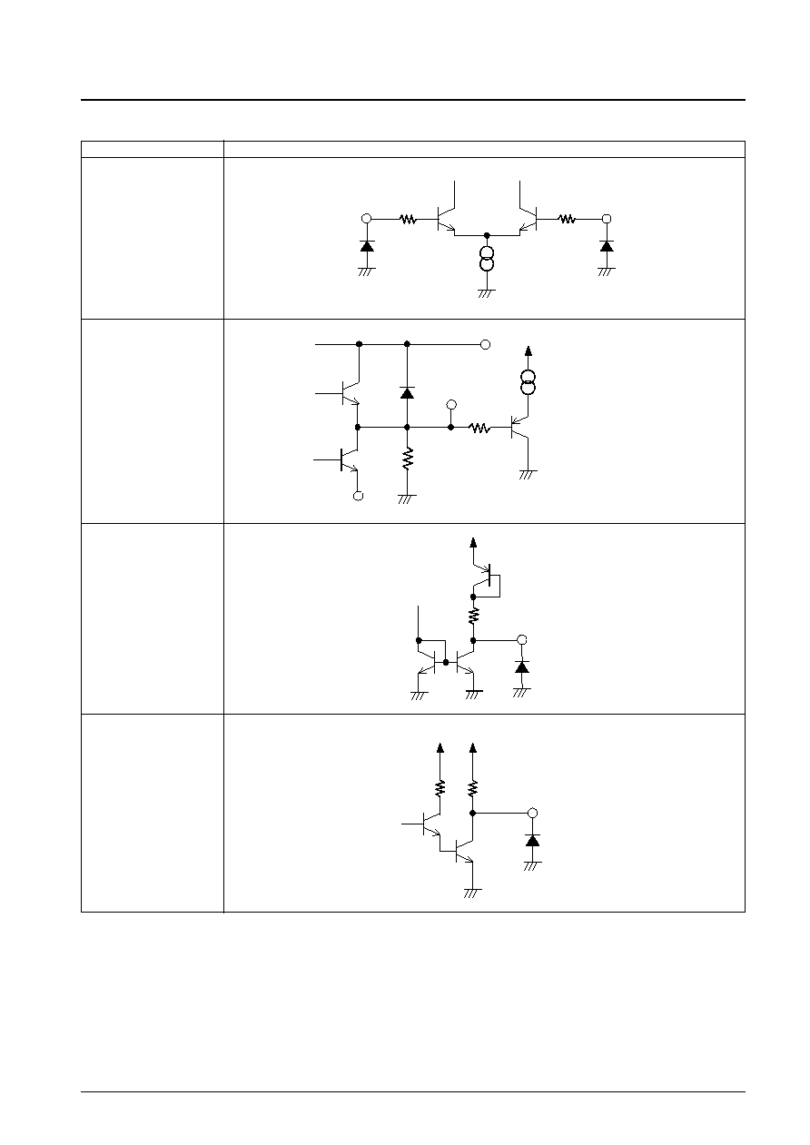
Equivalent Circuit Diagrams
Pin
Equivalent circuit diagrams
100
µ
A
200
200
Input (≠)
Input (+)
U
IN
(+)
U
IN
(≠)
V
IN
(+)
V
IN
(≠)
W
IN
(+)
W
IN
(≠)
200
Vs
Vcc
150
µ
A
30 k
RF
Output
Lower side oversaturation
prevention circuit input block
Vcc
FC
10 k
5 k
Vcc
300
FGOUT
10 k
Vcc
U ≠ OUT
V ≠ OUT
W ≠ OUT
RF
V
S
FC
FGOUT
No. 6212-5/6
LB11987
FC
UOUT
VOUT
WOUT
LIMREF
Bandgap 1.2V
UIN+
UIN≠
VIN+
VIN≠
WIN≠
WIN+
VCC
VS
UIN≠
GND
FGOUT
5K
RF
0.1
µ
0.1
µ
◊
3
0.5
VCC
UIN+
VCC
13.6k
30k
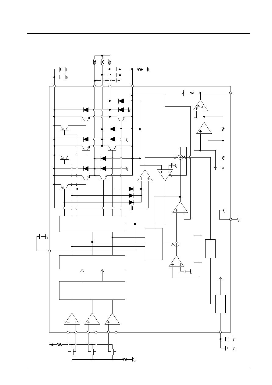
Block Diagram
Hall input synthesis block (linear matrix)
Schmitt
amplifier
Synthesized output logarithmic
compression block
Reference
voltage
Current limiter
Logarithmic conversion and differential
distribution
Differential
distribution
Feedback
amplifier
Upper side saturation
prevention control
Drive distribution circuit and
lower side saturation
prevention control
FG amplifier
Units (capacitance: F, resistance:
)
TSD

PS No.6212-6/6
LB11987
This catalog provides information as of July, 1999. Specifications and information herein are subject to
change without notice.
Specifications of any and all SANYO products described or contained herein stipulate the performance,
characteristics, and functions of the described products in the independent state, and are not guarantees
of the performance, characteristics, and functions of the described products as mounted in the customer's
products or equipment. To verify symptoms and states that cannot be evaluated in an independent device,
the customer should always evaluate and test devices mounted in the customer's products or equipment.
SANYO Electric Co., Ltd. strives to supply high-quality high-reliability products. However, any and all
semiconductor products fail with some probability. It is possible that these probabilistic failures could
give rise to accidents or events that could endanger human lives, that could give rise to smoke or fire,
or that could cause damage to other property. When designing equipment, adopt safety measures so
that these kinds of accidents or events cannot occur. Such measures include but are not limited to protective
circuits and error prevention circuits for safe design, redundant design, and structural design.
In the event that any or all SANYO products (including technical data, services) described or contained
herein are controlled under any of applicable local export control laws and regulations, such products must
not be exported without obtaining the export license from the authorities concerned in accordance with the
above law.
No part of this publication may be reproduced or transmitted in any form or by any means, electronic or
mechanical, including photocopying and recording, or any information storage or retrieval system,
or otherwise, without the prior written permission of SANYO Electric Co., Ltd.
Any and all information described or contained herein are subject to change without notice due to
product/technology improvement, etc. When designing equipment, refer to the "Delivery Specification"
for the SANYO product that you intend to use.
Information (including circuit diagrams and circuit parameters) herein is for example only; it is not
guaranteed for volume production. SANYO believes information herein is accurate and reliable, but
no guarantees are made or implied regarding its use or any infringements of intellectual property rights
or other rights of third parties.