 | –≠–ª–µ–∫—Ç—Ä–æ–Ω–Ω—ã–π –∫–æ–º–ø–æ–Ω–µ–Ω—Ç: LB1823M | –°–∫–∞—á–∞—Ç—å:  PDF PDF  ZIP ZIP |
Ordering number : EN4696B
13097HA(OT)/83095HA (OT) No. 4696-1/11
SANYO Electric Co.,Ltd. Semiconductor Bussiness Headquarters
TOKYO OFFICE Tokyo Bldg., 1-10, 1 Chome, Ueno, Taito-ku, TOKYO, 110 JAPAN
Monolithic Digital IC
LB1823M
SANYO Electric Co.,Ltd. Semiconductor Bussiness Headquarters
TOKYO OFFICE Tokyo Bldg., 1-10, 1 Chome, Ueno, Taito-ku, TOKYO, 110 JAPAN
Power Brushless Motor Predriver IC
for OA Applications
Overview
The LB1823M is a predriver IC developed for driving
power brushless motors in office automation applications.
A motor driver circuit with the desired output power
(current and voltage) can be constructed by attaching
either a driver array or discrete components at the output.
The LB1823M output supports direct PWM drive and thus
allows the implementation of low-loss drive circuits.
Additionally, the LB1823M includes several associated
circuits, such as a speed control circuit, and FG amplifier,
and an integrating amplifier, on chip.
Features
∑ Direct PWM drive output
∑ Crystal oscillator circuit
∑ Speed discriminator plus PLL speed control system
∑ Lock detector output
∑ Forward/reverse switching circuit
∑ Braking circuit (short braking technique)
∑ Start/stop switching circuit
∑ Over current limiter circuit (OCL)
∑ Thermal shutdown circuit (TSD)
∑ Built-in FG amplifier, integrating amplifier
∑ Shunt regulator output (7.0 V)
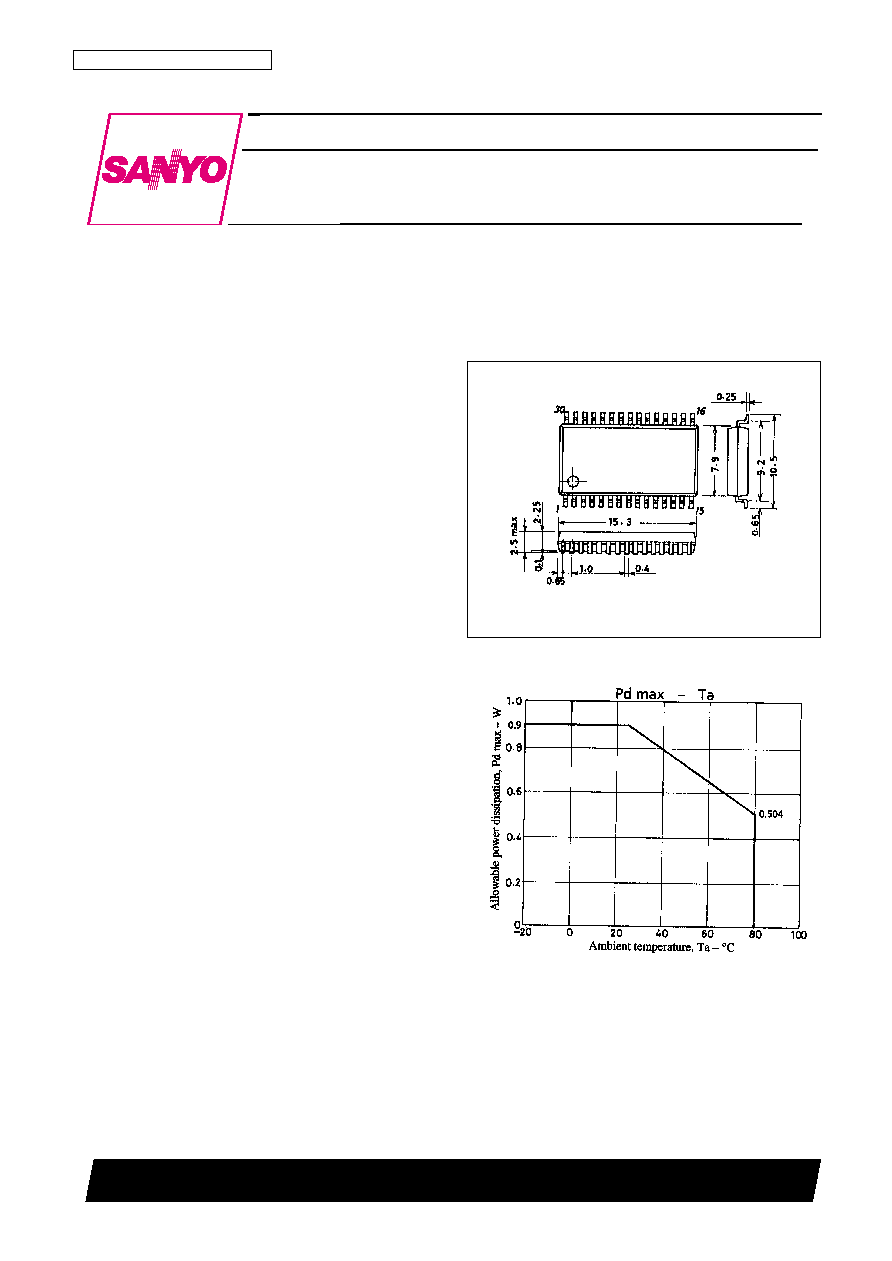
Package Dimensions
unit: mm
3073A-MFP30SD
SANYO: MFP30SD
[LB1823M]

Specifications
Absolute Maximum Ratings
at Ta = 25∞C
Allowable Operating Ranges
at Ta = 25∞C
Electrical Characteristics
at Ta = 25∞C, V
CC
= 6.3 V
No. 4696-2/11
LB1823M
Parameter
Symbol
Conditions
Ratings
Unit
Maximum supply voltage
V
CC
max
9
V
Maximum input current
I
REG
V
REG
pin
10
mA
Output current
I
O
UL, VL and WL outputs
30
mA
Allowable power dissipation
Pd max
0.9
W
Operating temperature
Topr
≠20 to +80
∞C
Storage temperature
Tstg
≠55 to +150
∞C
Parameter
Symbol
Conditions
Ratings
Unit
Input current range
I
REG
V
REG
pin (7 V)
1 to 5
mA
FG Schmitt output applied voltage
V
FGS
0 to 8
V
FG Schmitt output current
I
FGS
0 to 5
mA
Lock detector output current
I
LD
0 to 20
mA
Supply voltage
V
CC
4.5 to 7
V
Parameter
Symbol
Conditions
min
typ
max
Unit
Current drain
I
CC
1
33
50
mA
I
CC
2
When stopped
15
25
mA
Output saturation voltage
V
O
sat
UL, VL and WL outputs: I
O
= 20 mA
0.2
0.7
V
Output current
I
O
UH, VH and WH outputs: V
OUT
= 1.4 V
8
12
16
mA
Output leakage current
I
O
leak
UL, VL and WL outputs
100
µA
Output off voltage
V
O
off
UH, VH and WH outputs
0.5
V
[Hall Amplifier]
Input bias current
I
HB
≠4
≠1
µA
Common-mode input
V
ICM
1.5
4.4
V
voltage range
Hall input sensitivity
V
IN
60
mVp-p
Hysteresis
V
IN
17
32
60
mV
Input voltage low to high
V
SLH
16
mV
Input voltage high to low
V
SHL
≠16
mV
[Oscillator]
Output high level voltage
V
OH (CR)
3.1
3.4
3.7
V
Output low level voltage
V
OL (CR)
1.2
1.5
1.8
V
Oscillator frequency
f
(CR)
R = 56 k
, C = 1500 pF
20
kHz
Amplitude
V
(CR)
2.0
Vp-p
[Current Limiter Operation]
Limiter
V
RF
0.4
0.5
0.6
V
[Thermal Shutdown Operation]
Thermal shutdown operating
TSD
Design target
150
180
∞C
temperature
Hysteresis
TSD
Design target
30
∞C
[V
REG
Pin]
V
REG
pin voltage
V
REG
6.6
7.0
7.3
V
Continued on next page.
Continued from preceding page.
No. 4696-3/11
LB1823M
Parameter
Symbol
Conditions
min
typ
max
Unit
[FG Amplifier]
Input offset voltage
V
IO (FG)
≠10
+10
mV
Input bias current
I
B (FG)
≠1
+1
µA
Output high level voltage
V
OH (FG)
4.8
5.3
V
Output low level voltage
V
OL (FG)
1
1.5
V
FG input sensitivity
Gain: 100
◊
3
mV
Schmitt amplitude for the
100
180
250
mV
next stage
Operating frequency range
2
kHz
Open-loop gain
f
(FG)
= 2 kHz
45
51
dB
[FGS Output]
Output saturation voltage
V
O (FGS)
I
O (FGS)
= 2 mA
0.1
0.5
V
Output leakage current
I
L (FGS)
V
O
= V
CC
10
µA
[Speed Discriminator]
Output high level voltage
V
OH (D)
5.3
5.6
V
Output low level voltage
V
OL (D)
0.4
1.1
V
[PLL Output]
Output high level voltage
V
OH (P)
4.05
4.35
4.65
V
Output low level voltage
V
OL (P)
1.85
2.15
2.45
V
Number of counts
512
[Lock Detector]
Output low level voltage
V
OL (LD)
I
LD
= 10 mA
0.1
0.5
V
Output leakage current
I
L (LD)
V
O
= V
CC
10
µA
Lock range
±6.25
%
[Integrator]
Input bias current
I
B (INT)
≠0.4
+0.4
µA
Output high level voltage
V
OH (INT)
5.0
5.6
V
Output low level voltage
V
OL (INT)
0.8
1.2
V
Open-loop gain
60
dB
Gain bandwidth product
1.6
MHz
Reference voltage
≠5%
V
CC
/2
5%
V
[Crystal Oscillator]
Crystal oscillator frequency
f
OSC
Crystal oscillator
1
10
MHz
External input frequency
f
CLK
External signal input
1
10.2
MHz
[S/S Pin]
Input high level voltage
V
IH (S/S)
4.0
3.05
V
Input low level voltage
V
IL (S/S)
2.60
1.5
V
Hysteresis
V
IN
0.45
V
Pull-up resistor
R
U (S/S)
63
k
[F/R Pin]
Input high level voltage
V
IH (F/R)
4.0
3.05
V
Input low level voltage
V
IL (F/R)
2.60
1.5
V
Hysteresis
V
IN
0.45
V
Pull-down resistor
R
D (F/R)
30
50
70
k
[BR Pin]
Input high level voltage
V
IH (BR)
4.0
3.05
V
Input low level voltage
V
IL (BR)
2.60
1.5
V
Hysteresis
V
IN
0.45
V
Pull-down resistor
R
D (BR)
30
50
70
k

Pin Assignment
Block Diagram
No. 4696-4/11
LB1823M

Sample Application Circuit
Truth Table
Note: High (H) for a given input (IN) specifies the state where IN
+
> IN
≠
.
The formula below gives the relationship between the crystal oscillator frequency (f
OSC
) and the FG frequency (f
FG
).
f
FG
(servo) = f
OSC
/(ECL16 divisor
◊
number of counts)
= f
OSC
/8192
No. 4696-5/11
LB1823M
Item
F/R = L
F/R = H
Output
IN1
IN2
IN3
IN1
IN2
IN3
Source
Sink
1
H
L
H
L
H
L
VH
UL
2
H
L
L
L
H
H
WH
UL
3
H
H
L
L
L
H
WH
VL
4
L
H
L
H
L
H
UH
VL
5
L
H
H
H
L
L
UH
WL
6
L
L
H
H
H
L
VH
WL
Unit (capacitance: F)

No. 4696-6/11
LB1823M
External Crystal Oscillator Circuit
External Constants (reference value, V
CC
= 6.3 V)
External Constants (reference value, V
CC
= 5 V)
Note: However, an oscillator element with crystal fundamental frequency f
O
impedance to 3f
O
impedance ratio = 1:5 or greater must be used.
Xtal (MHz)
C1(pF)
C2(pF)
R(
)
3 to 4
39
120
390
4 to 5
39
120
560
5 to 7
39
82
820
7 to 10
39
68
2200
Xtal (MHz)
C1(pF)
C2(pF)
R(
)
3 to 4
39
180
330
4 to 5
39
150
390
5 to 7
39
100
560
7 to 10
39
68
1200
Pin Functions
Pin No.
Symbol
Function
30, 29
IN1
+
, IN1
≠
Hall input pin
28, 27
IN2
+
, IN2
≠
Hall input pin
26, 25
IN3
+
, IN3
≠
Hall input pin
19
UH
Output pin, constant current source output
21
VH
Output pin, constant current source output
23
WH
Output pin, constant current source output
18
UL
Output pin, open collector sink output
20
VL
Output pin, open collector sink output
22
WL
Output pin, open collector sink output
17
V
CC
Power supply
16
V
REG
7 V shunt regulator output
24
GND
Ground
4
CR
PWM oscillator frequency setting
9
INT
IN
Integrator input
10
INT
OUT
Integrator output (speed control pin)
7
D
OUT
Speed discriminator output. High on overspeed.
6
P
OUT
PLL output
8
LD
Lock detector
Low when the motor speed is in the lock range (±6.25%)
11
FG
IN+
FG pulse input (1/2 of the V
CC
voltage)
12
FG
IN≠
FG pulse input
13
FG
OUT
FG amplifier output
14
FGS
OUT
FG amplifier output (following the Schmitt circuit)
5
X'tal
Crystal oscillator. Connect a crystal oscillator element to this pin.
15
RF
Output current detection
1
S/S
Start/stop control pin
Low for start, high or open for stop
2
F/R
Forward/reverse control
Low or open for forward, high for reverse
3
BR
Brake, short brake
Low or open for start, high for brake. The S/S pin must be set to the stop state when releasing the brake.

External Component Functions
Notes on LB1823M Operation and External Components
1. Speed control circuit
The LB1823M uses a speed discriminator circuit and a PLL circuit in combination for speed control. The speed
discriminator generates an error output once every two FG periods using a charge pump technique. The PLL circuit
generates a phase error output once every FG period, also using a charge pump technique. By using a speed
discriminator circuit and a PLL circuit together, the LB1823M can suppress speed variations better than earlier
systems that only used a speed discriminator for speed control when used with motors faced with large load
variations. Since the following formula determines the FG servo frequency, the motor speed is set by the number of
FG pulses and the crystal oscillator frequency.
f
FG
(servo) = f
OSC
/8192
f
OSC
: Crystal oscillator frequency
2. Direct PWM drive
This IC adopts a direct PWM drive technique to minimize power loss in the outputs. The output transistors are
always saturated when on, and the motor drive power is adjusted by changing the duty with which the outputs are on.
Since the upper side transistors switch the outputs, Schottky, fast recovery, or similar diodes must be inserted
between OUT and ground (diodes D1, D2 and D3). (This is because through currents will flow in the upper side
transistors at the instant they turn on if these diodes do not have a short reverse recovery time.) Ordinary rectifying
diodes can be used between OUT and V
CC
. Transistors with no parasitic diodes must be used for the output lower
side transistors. If these transistors include parasitic diodes, through currents will flow due to their reverse recovery
time, even if Schottky diodes are used for D1, D2 and D3.
3. Current limiter circuit
The current limiter circuit operates (to limit the peak current) at a current determined by the formula I = 0.5/R
f
(where R
f
= R10). The limiting operation suppresses the current by reducing the on-duty. No phase compensation
capacitor is required.
No. 4696-7/11
LB1823M
Part
Function
Description
C1
Power supply stabilization
Choose a value such that the voltage fluctuations due to the motor drive currents are
stabilized.
C2
IC power supply stabilization
Attach as close as possible to pins 17 and 24.
R1, C3
PWM frequency setting
Use a resistor of 30 k
or larger for R1.
C4, C5, R2
External crystal oscillator circuit
See the figure on page 6.
C6, C7, R3, R4, R5
Servo constants
IC internal power supply
If the capacitance of this capacitor is too small, it will become harder to reset the internal IC
C8
stabilization
logic reliably and incorrect logic operation may occur. Attach as close as possible to pins 11
Reset pulse generation
and 24.
C9, C10, R7, R8
FG amplifier gain and frequency
characteristics settings
R10
Limit current setting
Output current I
OUT
= V
RF
/R10
R11, R12
Hall element bias current settings
R13, R14, R15
Sink current settings
These resistors set the sink currents for the UL, VL and WL (open collector) outputs.
R16
Shunt regulator bias current
Select a value such that a current of over 1 mA flows in the V
M
voltage range for which
settings
guaranteed correct operation is desired.
R17, R18, R19
Pull-down resistors
These resistors speed up the motor drive output transistor off times.
R20
Start time assurance
Include R20 in applications in which the start up time is a problem.
D1, D2, D3
Regeneration current absorption
Use Schottky diodes for D1, D2 and D3.

4. Speed lock range
The speed lock range is ±6.25% of the rated speed, and the LD pin (which is an open collector output) will be low
when the motor speed is within the lock range. The LB1823M controls the motor speed to be within the lock range
by generating a speed error signal when the motor speed goes out of the lock range and adjusting the motor drive on
duty according to that signal.
5. PWM frequency
The PWM frequency is determined by R1 and C3, which are connected to the CR pin.
When R1 is connected to a 6.3 V power supply (the application circuit pin 17 voltage):
f
PWM
1/(0.6 ∑ C ∑ R)
R1 must not be any smaller than 30 k
. A PWM frequency of 15 kHz is desirable. If the PWM frequency is too low,
the motor will resonate at the PWM frequency during motor constraint. This can result in disturbing audible
frequency noise. Inversely, the output transistor switching loss can become significant if the PWM frequency is too
high.
6. Grounding
The signal system ground must be separated from the output system ground, and these grounds must be connected to
a single ground point at the connector. The output system ground should be kept as short as possible since it carries
large current.
Output system ground ≠ ≠ The R
f
(R10) ground side. The D1, D2, and D3 ground side.
Signal system ground ≠ ≠ The IC pin 24 and the IC peripheral circuit ground.
7. External interface pins
∑ LD pin
Output type: open collector
Breakdown voltage:8 V
Manufacturing variation in the saturation voltage (reference value at I
LD
= 10 mA)
0.10 to 0.30 V
∑ FGS pin
Output type: open collector
Breakdown voltage: 8 V
Manufacturing variation in the saturation voltage (reference value at I
FGS
= 2 mA)
0.05 to 0.10 V
The FGS pin outputs the FG amplifier output converted to a pulse signal by a hysteresis comparator. Thus FGS is a
speed monitor output. No pull-up resistor is required when unused.
∑ S/S pin
Input type: PNP transistor base with a 63 k
pull-up resistor to V
CC
Threshold level: About 2.6 V (high to low), about 3.05 V (low to high)
(typical) Hysteresis: about 0.45 V
In the stop state, power is cut from all but certain circuits (the input, crystal oscillator and divider circuits) and the
LB1823M does not operate.
∑ F/R pin
Input type: PNP transistor base with a 50 k
pull-down resistor to ground
Threshold level: About 2.6 V (high to low), about 3.05 V (low to high)
(typical) Hysteresis: about 0.45 V
The forward/reverse direction must be switched in the stop state.
∑ BR pin
Input type: PNP transistor base with a 50 k
pull-down resistor to ground
Threshold level: About 2.6 V (high to low), about 3.05 V (low to high)
(typical) Hysteresis: about 0.45 V
Braking must be released in the stop mode.
No. 4696-8/11
LB1823M

8. FG amplifier
The FG amplifier gain is determined by R7 and R8, with the DC gain, G, being R8/R7. C9 and C10 determine the
FG amplifier frequency characteristics. (R7 and C9 form a high-pass filter and R8 and C10 form a low-pass filter.)
Since a Schmitt comparator is connected following the FG amplifier, the components R1, R2, C4 and C5 must be
chosen so that the amplitude is at least 250 mVp-p. (It is desirable that the FG output be set up to provide a level of
between 1 and 3 Vp-p during steady state motor rotation.)
9. Notes on external capacitors
∑ C8
C8 is required for stabilization of the FG
IN
+ pin constant voltage power supply and to generate the IC internal
logic reset pulse. The reset pulse is generated when the FG
IN
≠ pin reaches about 1.3 V from 0 V. If the reset does
not operate, the LD pin will go on briefly during IC start.
∑ C2
C2 is required for power supply stabilization. Since this IC adopts a PWM technique that switches large output
currents, it can generate noise extremely easily. Thus the power supply must be stabilized adequately so that this
noise does not cause the IC to operate incorrectly. C2 should be located as close as possible to pins 17 and 24.
10. Notes on external resistors
∑ R13, R14 and R15
These resistors set the external output (source side) transistor drive currents. The drive currents (I
D
) can be derived
from the following formula.
I
D
I
OUT
/h
FE
min
I
D
= (V
CC
≠ 0.7 ≠ V
O
sat)/R
I
OUT
: Maximum output current
h
FE
min: Output transistor minimum current amplification factor
V
O
sat: The LB1823M output saturation voltage
∑ R16
R16 sets the shunt regulator bias current. R16 must be selected so that a current of over 1 mA flows in the V
M
voltage range for which guaranteed correct operation is desired.
R16
(V
M
min ≠ V
REG
)/1 mA
∑ R17, R18 and R19
R17, R18 and R19 prevent leakage from the lower side output transistors and make the switching time faster.
∑ R20
R20 prevents leakage from the integrator. A value of around 24 k
is recommended. If this resistor is not used, the
INT OUT pin will go high in stop mode due to leakage currents. Startup is delayed by the integrator external time
constant at start time, since the motor is accelerated when the INTOUT pin is low.
11. External transistors
∑ Regulator transistor
Select a transistor with a current capacity of at least 70 mA and a breakdown voltage greater than the largest V
M
voltage. Heat generation will be a problem. Use a heat sink or other cooling technique if required.
Pd = (V
M
max ≠ V
REG
)
◊
I
I: I
CC
+ Hall bias current + output current (source) +
When the internal shunt regulator is not used, the power supply must be connected directly to the V
CC
pin
(4.5 to 7 V). The regulator transistor is not required in this case.
2SC2314 (TO126), 2SD330 (TO220)
2SC3985 (TO220ML) or similar transistor
∑ Output interface transistors
These transistors are used to assure that high voltages are not applied to the IC. (The total system cost is lower by
restricting the IC breakdown voltage.) Select transistors with a current capacity of at least 30 mA and a breakdown
voltage greater than the largest V
M
voltage. (R13, R14 and R15 determine the currents.)
2SC4641 (NP), 2SC4640 (SPA)
2SC4520 (PCP), 2SC4211 (MCP) or similar transistors
No. 4696-9/11
LB1823M
∑ Output transistors
The output transistors must be chosen according to the current and breakdown voltage settings determined by the
required motor power. Printed circuit board space considerations determine the choice of discrete or driver array
components.
The 2SC4070 (SPA) and 2SC4113 (SPA) lower side predriver transistors include an emitter-base resistor.
When no resistor is required, the same transistors as used in the output interface can be used.
Driver arrays:
SLA6022 and SLA6023 (Sanken)
12. Through currents due to the direct PWM technique
In the direct PWM technique through currents flow in the outputs due to the switching, e.g., when used in a discrete
structure (including predriver circuits) or in LB1822 applications. These trough currents are due to the delays and
parasitic capacitances in the output transistors. Although additional capacitors were previously used to deal with this
problem, the LB1823M includes circuit modifications to ameliorate through currents. However, even despite these
measures, through currents can still occur if the values of R17, R18 and R19 are made too large, since the switching
time of the lower side transistors will be increased. Although whiskers of under 10 ns can be seen in the R
f
voltage
waveform during switching, this will not be a problem. (These occur in the probe and do not correspond to current
flows.)
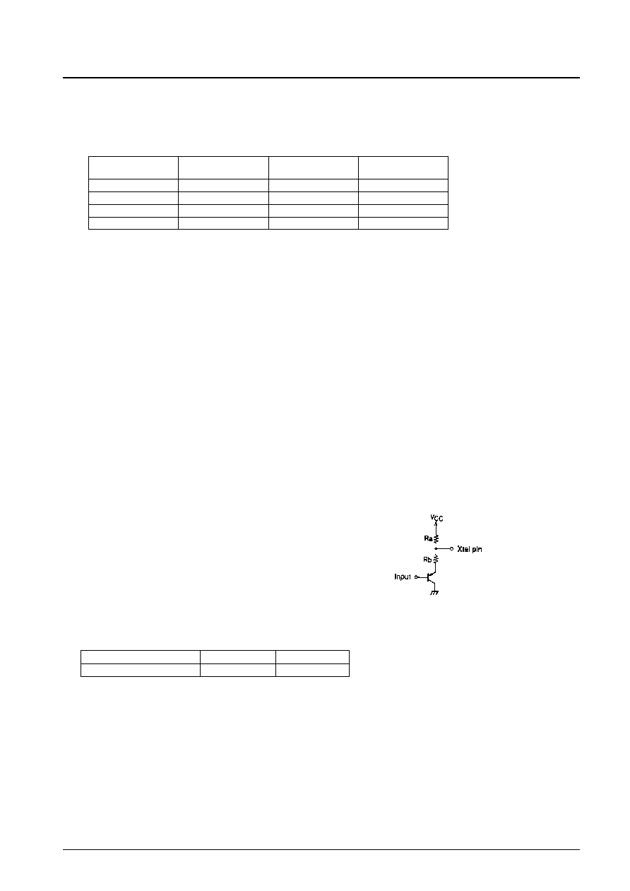
13. Oscillator element
Normally, a crystal resonator, a resistors, and two capacitors are connected to the LB1823M Xtal pin. A ceramic
oscillator could also be used in applications that do not require such precise speed control characteristics. To avoid
problems, consult with the manufacturer of the oscillator element when selecting the oscillator element and the
values of the external resistor and capacitors used. Use a circuit consisting of resistors and a pnp transistor as shown
in the figure to apply an external clock signal (CLK) to the Xtal pin.
f
CLK
= 1 to 10.2 MHz
Input signal levels
High level voltage: 4.0 V minimum
Low level voltage: 1.5 V maximum
Capacitors must be added to this circuit if overshoot
and/or undershoot appears in the input waveform. Be
sure to check for this condition in that case.
Reference values
No. 4696-10/11
LB1823M
Upper side transistors
Lower side transistors
Current
Breakdown voltage
(Darlington)
2SA1259
2SD1060
5 A
50 V
2SB881
2SD1061
7 A
50 V
2SB882
2SD1062
10 A
50 V
2SB883
2SD1065
15 A
50 V
V
CC
= 6.3 V typ (5.8 to 6.8 V)
Ra = 1.5 k
Rb = 2.0 k
V
CC
= 5.0 V typ (4.5 to 5.5 V)
Ra = 2.0 k
Rb = 1.0 k

No. 4696-11/11
LB1823M
14. Servo constants
The servo constant calculation varies significantly with the motor used, and requires specialized know-how. Thus
this should be handled by the motor manufacturer. We can provide the IC characteristics data required for the servo
constants calculations as well as frequency characteristics simulation data for the filter constants set by the motor
manufacturer. If the resistor between D
OUT
and INT.
IN
(R4) is too small, the values of C6 and C7 will become large.
If R4 is too large, speed errors will be likely to occur due to the speed discriminator cutoff current and the integrator
input current. Therefore, we think that a value in the range 10 to 100 k
is appropriate. If the resistor between P
OUT
and INT.
IN
(R3) is too small, the influence of the PLL system will be too large and pull-in to lock synchronization
will be degraded. Therefore, this resistor should not be too small. (We recommend a value of about 1 M
when R4
is 75 k
.) First determine the constants for the speed discriminator system only (R4, R5, C6 and C7), and then
determine the value of R3 in the PLL system.
This catalog provides information as of January, 1997. Specifications and information herein are subject to
change without notice.
s
No products described or contained herein are intended for use in surgical implants, life-support systems, aerospace
equipment, nuclear power control systems, vehicles, disaster/crime-prevention equipment and the like, the failure of
which may directly or indirectly cause injury, death or property loss.
s
Anyone purchasing any products described or contained herein for an above-mentioned use shall:
Accept full responsibility and indemnify and defend SANYO ELECTRIC CO., LTD., its affiliates, subsidiaries and
distributors and all their officers and employees, jointly and severally, against any and all claims and litigation and all
damages, cost and expenses associated with such use:
Not impose any responsibility for any fault or negligence which may be cited in any such claim or litigation on
SANYO ELECTRIC CO., LTD., its affiliates, subsidiaries and distributors or any of their officers and employees
jointly or severally.
s
Information (including circuit diagrams and circuit parameters) herein is for example only; it is not guaranteed for
volume production. SANYO believes information herein is accurate and reliable, but no guarantees are made or implied
regarding its use or any infringements of intellectual property rights or other rights of third parties.