 | –≠–ª–µ–∫—Ç—Ä–æ–Ω–Ω—ã–π –∫–æ–º–ø–æ–Ω–µ–Ω—Ç: LB1836M | –°–∫–∞—á–∞—Ç—å:  PDF PDF  ZIP ZIP |
Low-saturation, Bidirectional Motor Driver
for Low-voltage Applications
Overview
The LB1836M is a low-saturation two-channel bidirectional
motor driver IC for use in low-voltage applications.
The LB1836M is a bipolar stepper-motor driver IC that is ideal
for use in printers, FDDs, cameras and other portable devices.
Features
.
Low voltage operation (2.5 V min)
.
Low saturation voltage (upper transistor + lower transistor
residual voltage; 0.40 V typ at 400 mA).
.
Parallel connection
(Upper transistor + lower transistor residual voltage; 0.5 V
typ at 800 mA).
.
Separate logic power supply and motor power supply
.
Brake function
.
Spark killer diodes built in
.
Thermal shutdown circuit built in
.
Compact package (14-pin MFP)
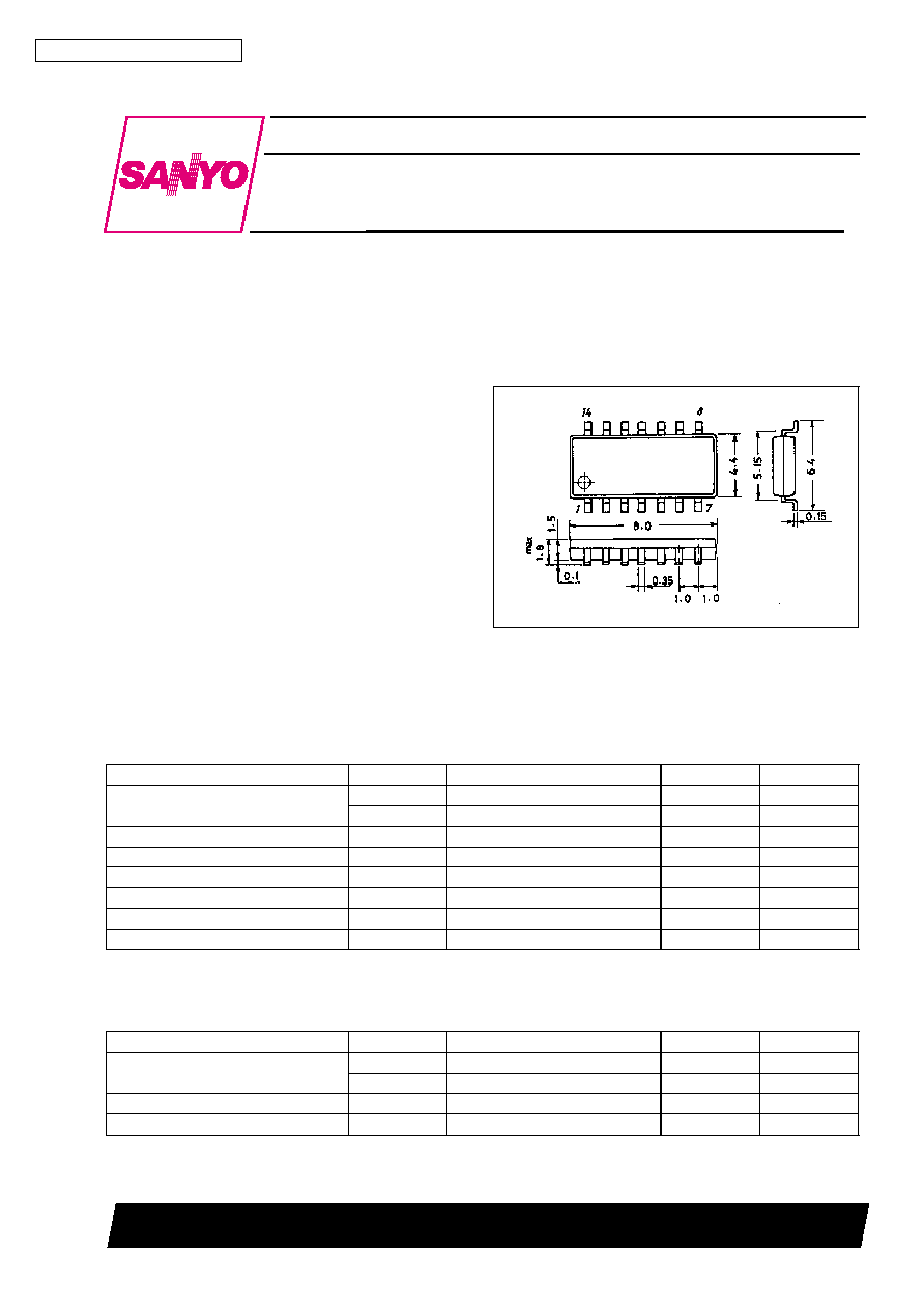
Package Dimensions
unit : mm
3111-MFP14S
[LB1836M]
SANYO : MFP14S
Specifications
Absolute Maximum Ratings
at Ta = 25∞C
Parameter
Symbol
Conditions
Ratings
Unit
Maximum supply voltage
V
CC
max
≠0.3 to +10.5
V
V
S
max
≠0.3 to +10.5
V
Output applied voltage
V
OUT
V
S
+ V
SF
V
Input applied voltage
V
IN
≠0.3 to +10
V
Ground pin flow-out current
IGND
Per channel
1.0
A
Allowable power dissipation
Pd max
*
With board
800
mW
Operating temperature
Topr
≠20 to +75
∞C
Storage temperature
Tstg
≠40 to +125
∞C
*Note: Mounted on 30
◊
30
◊
1.5 mm
3
glass epoxy PCB
Allowable Operating Ranges
at Ta = 25∞C
Parameter
Symbol
Conditions
Ratings
Unit
Supply voltage
V
CC
2.5 to 9.0
V
V
S
1.8 to 9.0
V
Input high-level voltage
V
IH
1.8 to 9.0
V
Input low-level voltage
V
IL
≠0.3 to +0.7
V
Ordering number: EN3947B
Monolithic Digital IC
LB1836M
SANYO Electric Co.,Ltd. Semiconductor Bussiness Headquarters
TOKYO OFFICE Tokyo Bldg., 1-10, 1 Chome, Ueno, Taito-ku, TOKYO, 110 JAPAN
21097HA(II)/D2293/O0693(US) No.3947-1/5
Electrical Characteristics
at Ta = 25∞C, V
CC
= V
S
= 3 V
Parameter
Symbol
Conditions
min
typ
max
Unit
Supply current
I
CC
0
V
IN
1, 2, 3, 4 = 0 V, I
CC
+ I
S
0.1
10
µA
I
CC
1
V
IN
1 = 3 V, V
IN
2, 3, 4 = 0 V, I
CC
+ I
S
14
20
mA
I
CC
2
V
IN
1, 2 = 3 V, V
IN
3, 4 = 0 V, I
CC
+ I
S
22
35
mA
Output saturation voltage
(upper + lower)
V
OUT
1
I
OUT
= 200 mA
0.2
0.28
V
V
OUT
2
I
OUT
= 400 mA
0.4
0.6
V
V
OUT
3
I
OUT
= 400 mA, parallel connection
0.25
0.35
V
V
OUT
4
I
OUT
= 800 mA, parallel connection
0.5
0.7
V
Output sustaining voltage
V
O
(sus)
I
OUT
= 400 mA
9
V
Input current
I
IN
V
IN
= 2 V, V
CC
= 6 V
80
µA
Spark killer diode reverse
current
Is (leak)
V
CC
1, 2 = 9 V
30
µA
Spark killer diode forward
voltage
V
SF
I
OUT
= 400 mA
1.7
V
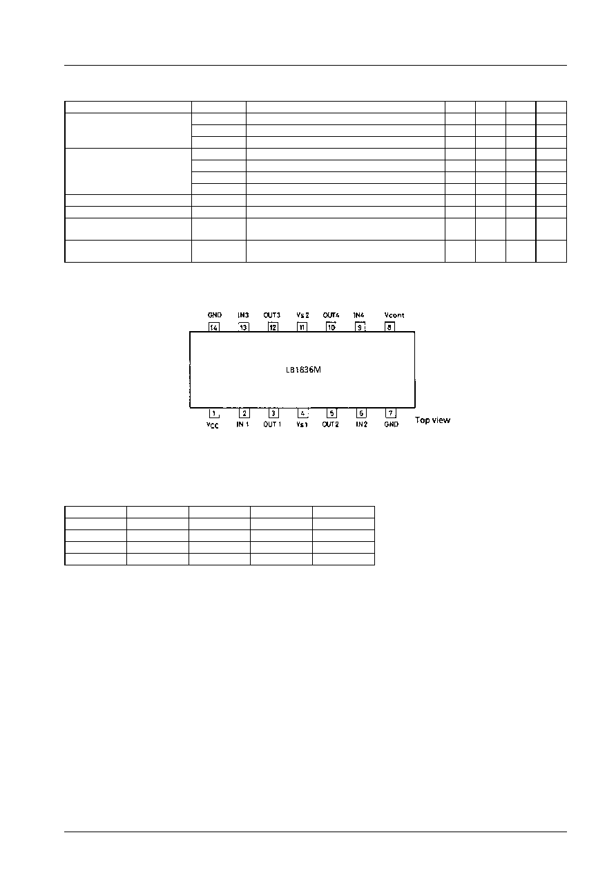
Pin Assignment
Truth Table
IN 1, 3
IN 2, 4
OUT 1, 3
OUT 2, 4
Mode
H
L
H
L
Forward
L
H
L
H
Reverse
H
H
L
L
Brake
L
L
OFF
OFF
Standby
Design Notes
If large current flows on the power supply (V
S
) line and the GND line, then in some applications and layouts, misoperation due to
line oscillation may result.
The modes during which large current flows are as follows:
.
Motor surge current when the DC motor starts up or when it shifts rotation directions (forward O reverse).
.
Passthrough current generated within the IC when shifting rotation directions (forward O reverse) or when shifting from
forward/reverse rotation to braking, or vice versa.
The following points should be kept in mind regarding the pattern layout:
.
Keep the wiring lines thick and short in order to reduce wiring inductance between the power supply (V
S
) and GND.
.
Insert a passthrough capacitor near the IC. (Maximum effect is obtained by inserting the passthrough capacitor between V
S
and
the pin 7 GND at the closest distance possible.
.
If the CPU and the LB1836M are mounted on separate boards and the difference between the ground potential of each board is
large, install resistors of about 10 k
in series between the CPU and the LB1836M inputs.
Note) Both GNDs must be connected. P-GND of OUT2 and OUT4 and S-GND of the
control section are connected to the pin 7 GND within the IC, and P-GND of OUT1
and OUT3 is connected to the pin 14 GND.
LB1836M
No.3947-2/5
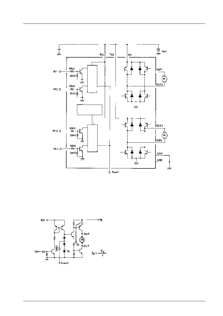
Block Diagram
Vcont pin
As shown in the above diagram, the Vcont pin outputs the voltage of the band gap Zener V
Z
+V
F
(= 1.93 V).
In normal use, this pin is left open.
The drive current I
D
is varied by the Vcont voltage. However, because the band gap Zener is shared, it functions as a bridge.
Control
Thermal
shutdown
Control
Note: As long as the voltages applied to V
CC
, V
S
1, V
S
2, and IN1 through IN4 are within the limits set by the absolute
maximum ratings, there are no restrictions on the relationship of each voltage level in comparison
with the others (regarding which is higher or lower). (ex. V
CC
= 3 V, V
S
1, 2 = 2 V, IN1 to IN4 = 5 V)
(= constant)
LB1836M
No.3947-3/5

Allowable
power
dissipation,
Pd
max
-
m
W
Ambient temperature, Ta - ∞C
Specified board (30
◊
30
◊
1.5 mm
3
glass epoxy )
Output
saturation
voltage,
V
O
(sat)
-
V
Output current, I
O
- mA
Input
current,
I
IN
-µ
A
Ambient temperature, Ta - ∞C
Ambient temperature, Ta - ∞C
Output
saturation
voltage,
V
O
(sat)
≠
V
total value
Output current, I
O
- mA
Output
saturation
voltage,
V
O
(sat)
≠
V
Current
drain,
I
S
≠m
A
Ambient temperature, Ta - ∞C
Break
Forward
Reverse
Parallel
connection total
Current
drain,
I
CC
≠m
A
Ambient temperature, Ta - ∞C
Input
current,
I
IN
-µ
A
Input voltage, V
IN
- V
Break
Forward
Reverse
LB1836M
No.3947-4/5
No products described or contained herein are intended for use in surgical implants, life-support systems, aerospace equipment,
nuclear power control systems, vehicles, disaster/crime-prevention equipment and the like, the failure of which may directly or
indirectly cause injury, death or property loss.
Anyone purchasing any products described or contained herein for an above-mentioned use shall:
1
Accept full responsibility and indemnify and defend SANYO ELECTRIC CO., LTD., its affiliates, subsidiaries and distributors
and all their officers and employees, jointly and severally, against any and all claims and litigation and all damages, cost and
expenses associated with such use:
2
Not impose any responsibility for any fault or negligence which may be cited in any such claim or litigation on SANYO
ELECTRIC CO., LTD., its affiliates, subsidiaries and distributors or any of their officers and employees jointly or severally.
Information (including circuit diagrams and circuit parameters) herein is for example only; it is not guaranteed for volume
production. SANYO believes information herein is accurate and reliable, but no guarantees are made or implied regarding its use
or any infringements of intellectual property rights or other rights of third parties.
This catalog provides information as of February, 1997. Specifications and information herein are subject to change without notice.
Current
drain,
I
CC
≠m
A
Break
Break
Forward/Reverse
Forward/Reverse
Supply voltage, V
S
≠ V
Supply voltage, V
CC
≠ V
Current
drain,
I
S
≠m
A
Standby
Standby
LB1836M
No.3947-5/5