73098HA (KT)/9050TA (KOTO) No.3659-1/6
SANYO Electric Co.,Ltd. Semiconductor Bussiness Headquaters
TOKYO OFFICE Tokyo Bldg., 1-10, 1 Chome, Ueno, Taito-ku, TOKYO, 110-8534 JAPAN
Any and all SANYO products described or contained herein do not have specifications that can handle
applications that require extremely high levels of reliability, such as life-support systems, aircraft's
control systems, or other applications whose failure can be reasonably expected to result in serious
physical and/or material damage. Consult with your SANYO representative nearest you before using
any SANYO products described or contained herein in such applications.
SANYO assumes no responsibility for equipment failures that result from using products at values that
exceed, even momentarily, rated values (such as maximum ratings, operating condition ranges,or other
parameters) listed in products specifications of any and all SANYO products described or contained
herein.
Monolithic Digital IC
3-Phase Brushless Motor Driver
Ordering number:EN3659
LB1851M
r
e
t
e
m
a
r
a
P
l
o
b
m
y
S
s
n
o
i
t
i
d
n
o
C
s
g
n
i
t
a
R
t
i
n
U
1
e
g
a
t
l
o
v
y
l
p
p
u
S
V C
C 1
0
.
6
o
t
0
.
4
V
2
e
g
a
t
l
o
v
y
l
p
p
u
S
V C
C 2
4
1
o
t
4
V
3
e
g
a
t
l
o
v
y
l
p
p
u
S
VS
V
o
t
p
u
C
C 2
V
r
e
t
e
m
a
r
a
P
l
o
b
m
y
S
s
n
o
i
t
i
d
n
o
C
s
g
n
i
t
a
R
t
i
n
U
1
e
g
a
t
l
o
v
y
l
p
p
u
s
m
u
m
i
x
a
M
V C
C
x
a
m
1
7
V
2
e
g
a
t
l
o
v
y
l
p
p
u
s
m
u
m
i
x
a
M
V C
C
x
a
m
2
6
1
V
3
e
g
a
t
l
o
v
y
l
p
p
u
s
m
u
m
i
x
a
M
VS
x
a
m
V C
C 2
V
e
g
a
t
l
o
v
y
l
p
p
u
s
t
u
p
t
u
O
VO
x
a
m
VS V
2
+
V
t
n
e
r
r
u
C
t
u
p
t
u
O
IO
x
a
m
5
.
1
A
n
o
i
t
a
p
i
s
s
i
d
r
e
w
o
p
e
l
b
a
w
o
ll
A
x
a
m
d
P
0
.
1
W
e
r
u
t
a
r
e
p
m
e
t
g
n
i
t
a
r
e
p
O
r
p
o
T
5
7
+
o
t
0
2
�
e
r
u
t
a
r
e
p
m
e
t
e
g
a
r
o
t
S
g
t
s
T
5
2
1
+
o
t
5
5
�
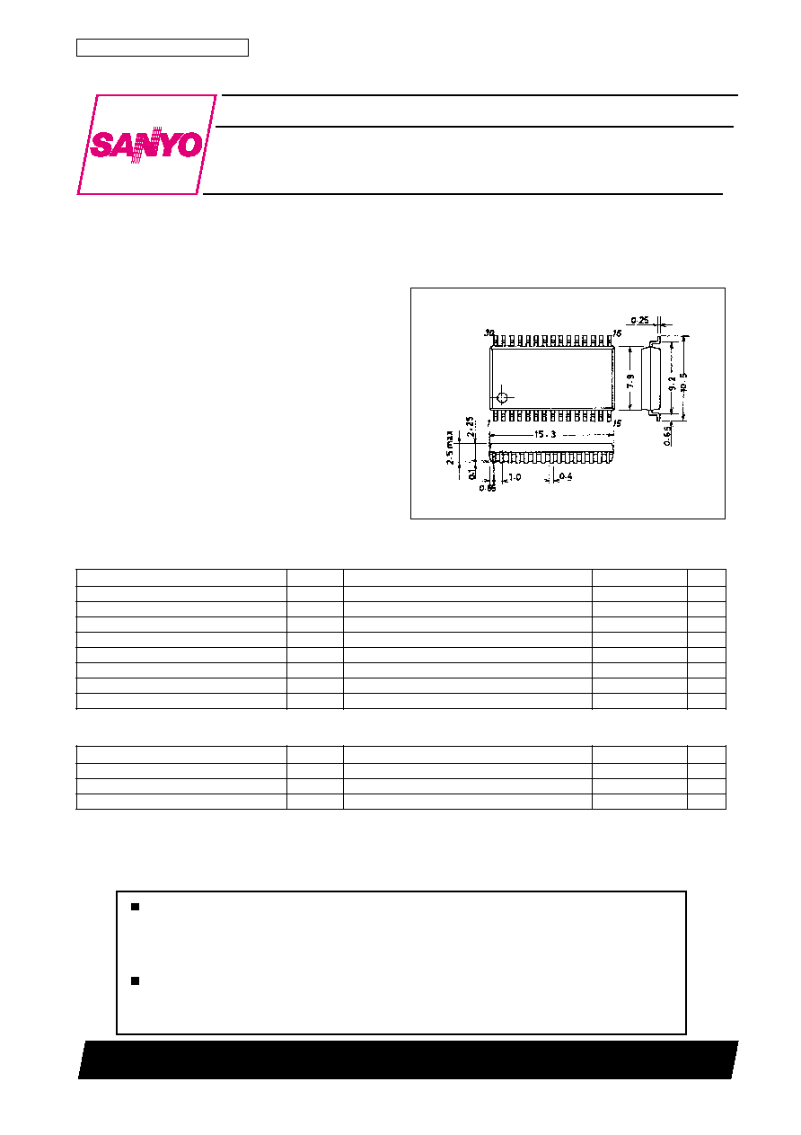
Package Dimensions
unit:mm
3073A-MFP30S
[LB1851M]
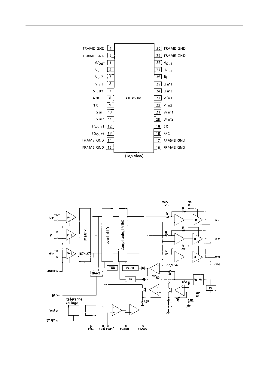
Overview
The LB1851M is a 3-phase brushless motor drive IC
ideally suited for use in VCR capstan motor driver, drum
motor driver, and DAT motor driver applications.
Features
� 120�C voltage linear type.
� Less power dissipation because of speed control based
on motor voltage control (suitable for use in portable
sets).
� Torque ripple compensation circuit on chip.
� Small capacitance of external capacitor because of soft
switching method (clip capacitor).
� Thermal shutdown circuit on chip.
� FG amplifier on chip.
Specifications
Absolute Maximum Ratings
at Ta = 25�C
�C
Absolute Operating Conditions
at Ta = 25�C
�C
SANYO : MFP30S

No.3659-2/6
LB1851M
Electrical Characteristics
at Ta = 25�C, V
CC
1=5V, V
CC
2=7V, V
S
=3V
r
e
t
e
m
a
r
a
P
l
o
b
m
y
S
s
n
o
i
t
i
d
n
o
C
s
g
n
i
t
a
R
t
i
n
U
n
i
m
p
y
t
x
a
m
1
t
n
e
r
r
u
c
y
l
p
p
u
S
I C
C 1
V R
B
V
5
=
5
.
4
5
.
6
A
m
2
t
n
e
r
r
u
c
y
l
p
p
u
S
I C
C 2
V R
B
V
5
=
5
1
0
2
A
m
3
t
n
e
r
r
u
c
y
l
p
p
u
S
IS
V R
B
R
,
V
5
=
L=
5
.
6
0
.
9
A
m
1
t
n
e
r
r
u
c
y
b
d
n
a
t
s
t
u
p
t
u
O
I
Q
O
C
C
V
Y
B
T
S
V
0
=
0
8
1
A
�
2
t
n
e
r
r
u
c
y
b
d
n
a
t
s
t
u
p
t
u
O
I
Q
O
S
V
Y
B
T
S
R
,
V
0
=
L=
0
5
1
A
�
e
g
a
t
l
o
v
n
o
i
t
a
r
u
t
a
s
t
u
p
t
u
O
V
)
t
a
s
(
O
I
T
U
O
e
c
r
u
o
s
+
k
n
i
s
,
A
0
.
1
=
3
.
2
V
e
g
a
t
l
o
v
S
R
T
t
u
p
t
u
O
V
)
s
u
s
(
O
I
T
U
O
A
m
0
2
=
6
1
*
V
e
g
a
t
l
o
v
y
b
d
n
a
t
s
t
u
p
t
u
O
V Q
O
I R
B
V
5
=
4
.
1
5
.
1
6
.
1
V
e
g
a
l
t
o
v
t
e
s
f
f
O
t
u
p
n
i
r
e
i
f
il
p
m
a
ll
a
H
V
t
e
s
f
f
o
H
5
�
5
+
*
V
m
e
g
n
a
r
e
g
a
t
l
o
v
t
u
p
n
I
e
d
o
m
-
n
o
m
m
o
c
r
e
i
f
il
p
m
a
ll
a
H
V
M
O
C
H
4
.
1
8
.
2
V
n
i
a
g
e
g
a
t
l
o
V
t
u
p
t
u
o
-
t
u
p
n
i
ll
a
H
G
O
H
V
k
2
.
8
=
e
l
g
n
a
R
5
.
1
3
5
.
4
3
5
.
7
3
B
d
e
g
a
t
l
o
v
l
e
v
e
l
-
'
H
'
n
i
p
e
k
a
r
B
0
.
2
V
e
g
a
t
l
o
v
l
e
v
e
l
-
'
L
'
n
i
p
e
k
a
r
B
8
.
0
V
t
n
e
r
r
u
c
t
u
p
n
i
n
i
p
e
k
a
r
B
0
0
1
A
�
t
n
e
r
r
u
c
e
g
a
k
a
e
l
n
i
p
e
k
a
r
B
0
3
�
A
�
e
g
a
t
l
o
v
l
e
v
e
l
-
'
H
'
n
i
p
C
R
F
8
.
2
V
e
g
a
t
l
o
v
l
e
v
e
l
-
'
L
'
n
i
p
C
R
F
2
.
1
V
t
n
e
r
r
u
c
t
u
p
n
i
n
i
p
C
R
F
0
0
1
A
�
t
n
e
r
r
u
c
e
g
a
k
a
e
l
n
i
p
C
R
F
0
3
�
A
�
e
g
a
t
l
o
v
l
a
u
d
i
s
e
r
r
e
p
p
U
V H
X
I
T
U
O
V
,
A
m
0
0
1
=
C
C
V
,
V
6
=
2
S
V
2
=
8
3
.
0
5
5
.
0
V
e
g
a
t
l
o
v
l
a
u
d
i
s
e
r
r
e
w
o
L
V L
X
I
T
U
O
V
,
A
m
0
0
1
=
C
C
V
,
V
6
=
2
S
V
2
=
1
4
.
0
5
.
0
V
t
n
i
o
p
n
o
i
t
c
e
l
f
n
i
e
g
a
t
l
o
v
l
a
u
d
i
s
e
R
0
.
2
V
t
n
u
o
m
a
p
a
l
r
e
v
O
V C
C
V
,
V
6
=
2
S
V
3
=
0
6
0
7
0
8
%
e
g
a
t
l
o
v
N
O
y
b
d
n
a
t
S
2
.
0
�
1
.
0
+
V
e
g
a
t
l
o
v
F
F
O
y
b
d
n
a
t
S
)
1
e
t
o
n
(
f
f
o
y
b
d
n
a
t
s
:
n
e
p
O
2
5
V
t
n
e
r
r
u
c
s
a
i
b
n
i
p
y
b
d
n
a
t
S
D
N
G
n
i
P
0
1
A
�
f
o
e
r
u
t
a
r
e
p
m
e
t
g
n
i
t
a
r
e
p
O
t
i
u
c
r
i
c
n
w
o
d
t
u
h
s
l
a
m
r
e
h
t
0
5
1
0
8
1
0
1
2
t
i
u
c
r
i
c
n
w
o
d
t
u
h
s
l
a
m
r
e
h
t
f
o
s
i
s
e
r
e
t
s
y
H
5
1
]
r
e
i
f
il
p
m
A
G
F
[
e
g
a
t
l
o
v
t
e
s
f
f
o
t
u
p
n
i
r
e
i
f
il
p
m
a
G
F
V
t
e
s
f
f
o
G
F
8
�
8
+
V
m
n
i
a
g
e
g
a
t
l
o
v
p
o
o
l
n
e
p
O
G
G
F
V
z
H
k
1
=
f
0
6
B
d
e
g
a
t
l
o
v
n
o
i
t
a
r
u
t
a
s
t
u
p
t
u
o
e
d
i
s
e
c
r
u
o
S
V
T
U
O
G
F
IO
A
m
2
�
=
7
.
3
V
e
g
a
t
l
o
v
n
o
i
t
a
r
u
t
a
s
t
u
p
t
u
o
e
d
i
s
k
n
i
S
V G
F
D
O
IO
A
m
2
=
3
.
1
V
n
o
i
t
c
e
j
e
r
l
a
n
g
i
s
e
d
o
m
-
n
o
m
m
o
C
R
H
C
0
8
*
B
d
e
g
n
a
r
e
g
a
t
l
o
v
t
u
p
n
i
e
d
o
m
-
n
o
m
m
o
c
r
e
il
i
p
m
a
G
F
V
H
C
G
F
0
5
.
3
V
n
i
g
r
a
m
e
s
a
h
P
0
2
e
g
a
t
l
o
v
d
l
o
h
s
e
r
h
t
r
e
i
f
il
p
m
a
t
t
i
m
h
c
S
V
n
i
G
F
V
,
V
5
.
2
=
+
T
U
O
G
F
L
o
t
H
t
a
2
5
4
.
2
0
5
.
2
5
5
.
2
V
s
i
s
e
r
e
t
s
y
h
r
e
i
f
il
p
m
a
t
t
i
m
h
c
S
V
n
i
G
F
V
5
.
2
=
+
0
2
0
4
0
6
V
m
�C*
�C*
Note1 : When standby pin is left open, standby operation is turned to off.
Note2*: Values shown are design targets only. No measurements have been taken. Overlap spec. are regarded as test
specification.
�C*
No.3659-3/6
LB1851M
Pin Assignment
Block Diagram

No.3659-4/6
LB1851M
e
d
o
M
e
c
r
u
o
S
k
n
i
S
t
u
p
n
I
e
s
r
e
v
e
R
/
d
r
a
w
r
o
F
l
o
r
t
n
o
C
U
V
W
1
e
s
a
h
p
W
e
s
a
h
p
V
H
H
L
L
e
s
a
h
p
V
e
s
a
h
p
W
H
2
e
s
a
h
p
W
e
s
a
h
p
U
H
L
L
L
e
s
a
h
p
U
e
s
a
h
p
W
H
3
e
s
a
h
p
V
e
s
a
h
p
W
L
L
H
L
e
s
a
h
p
W
e
s
a
h
p
V
H
4
e
s
a
h
p
U
e
s
a
h
p
V
L
H
L
L
e
s
a
h
p
V
e
s
a
h
p
U
H
5
e
s
a
h
p
V
e
s
a
h
p
U
H
L
H
L
e
s
a
h
p
U
e
s
a
h
p
V
H
6
e
s
a
h
p
U
e
s
a
h
p
W
L
H
H
L
e
s
a
h
p
W
e
s
a
h
p
U
H
Sample Application Circuit
Truth Table
Input : "H" : Input 1 of each phase is at a potential which is higher by more than 0.2V relative to input 2.
"L" : Input 1 of each phase is at a potential which is lower by more than 0.2V relative to input 2.
Forward/reverse control : "H" :2.8V to V
CC
1
"L" : 0V to 1.2V
No.3659-5/6
LB1851M
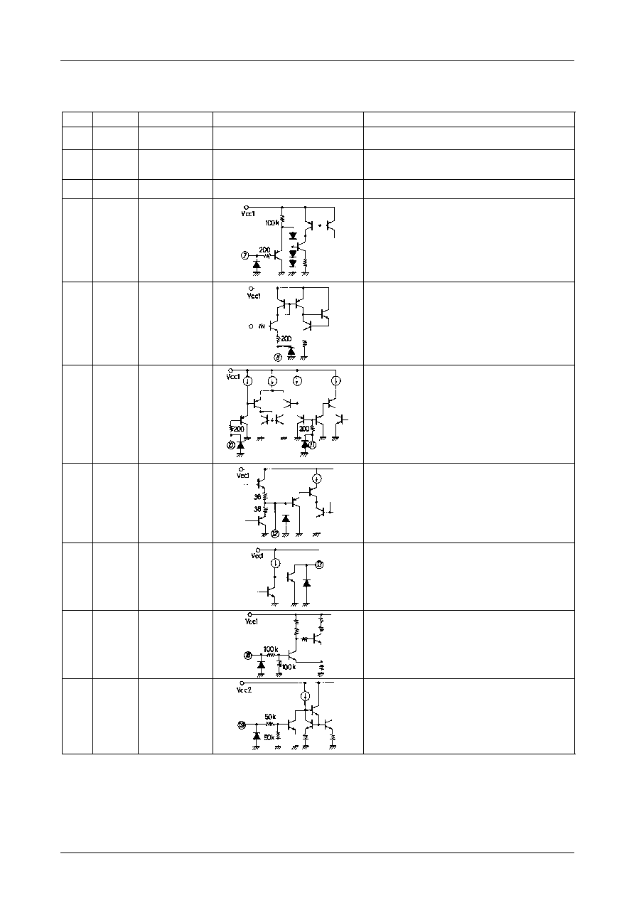
Pin Description
Pin No.
4
5
6
7
8
12
13
18
10
11
Symbol
Pin voltage
Equivalent circuit
Pin function
V
S
V
CC
2
<V
CC
2
4V to 14V
V
CC
1
4V to 6V
ST. BY
ANGLE
L : 0.1V max
H : 2.0V min
(When V
CC
1=5V)
L : 1.2V max
H : 2.8V min
(When V
CC
1=5V)
min 0V
max 3.5V
(When V
CC
1=5V)
FG in�
FG in+
FG
OUT
1
FG
OUT
2
FRC
Power supply pin for fixing the output amplitude. Must be lower
than V
CC
2 voltage.
Power supply pin for amp circuit other than motor driver
transistor. Power supply pin for supplying voltage to other than
the control section whose supply voltage is V
CC
1.
Power supply pin for supplying voltage to the hall amp, forward
/reverse control, FG amp, thermal shutdown circuit.
When this pin is grounded, all the circuitry stops operating.
In this case, the supply current is approximately 100
�
A. In the
normal operation mode, this pin is left open or made to be at a
potential of more than 2V.
The hall input-output gain (slope of motor waveform) can be
changed by changing the resistance connected across this pin
and GND.
FG signal input pin.
FG amp output pin.
FG schmitt amp output pin.
Pin for forward/reverse control of motor
L level : Forward (Less than 1.2V : When V
CC
1=5V)
H level : Reverse (More than 2.8V : When V
CC
1=5V).
19
BR
L : 0.8V max
H : 2.0V min
Pin for stopping the motor
L level : Motor drive (Less than 0.8V).
H level : Motor stop (More than 2.0V).
Unit (resistance :
)

PS No.3659-6/6
Specifications of any and all SANYO products described or contained herein stipulate the performance,
characteristics, and functions of the described products in the independent state, and are not guarantees
of the performance, characteristics, and functions of the described products as mounted in the customer's
products or equipment. To verify symptoms and states that cannot be evaluated in an independent device,
the customer should always evaluate and test devices mounted in the customer's products or equipment.
SANYO Electric Co., Ltd. strives to supply high-quality high-reliability products. However, any and all
semiconductor products fail with some probability. It is possible that these probabilistic failures could
give rise to accidents or events that could endanger human lives, that could give rise to smoke or fire,
or that could cause damage to other property. When designing equipment, adopt safety measures so
that these kinds of accidents or events cannot occur. Such measures include but are not limited to protective
circuits and error prevention circuits for safe design, redundant design, and structural design.
In the event that any and all SANYO products described or contained herein fall under strategic
products (including services) controlled under the Foreign Exchange and Foreign Trade Control Law of
Japan, such products must not be exported without obtaining export license from the Ministry of
International Trade and Industry in accordance with the above law.
No part of this publication may be reproduced or transmitted in any form or by any means, electronic or
mechanical, including photocopying and recording, or any information storage or retrieval system,
or otherwise, without the prior written permission of SANYO Electric Co. , Ltd.
Any and all information described or contained herein are subject to change without notice due to
product/technology improvement, etc. When designing equipment, refer to the "Delivery Specification"
for the SANYO product that you intend to use.
Information (including circuit diagrams and circuit parameters) herein is for example only ; it is not
guaranteed for volume production. SANYO believes information herein is accurate and reliable, but
no guarantees are made or implied regarding its use or any infringements of intellectual property rights
or other rights of third parties.
This catalog provides information as of July, 1998. Specifications and information herein are subject to
change without notice.
LB1851M
Pin No.
26
27
28
3
1,2
14,15
16,17
29,30
U
OUT
V
OUT
W
OUT
Symbol
Pin voltage
Equivalent circuit
Pin function
Rf
FRAME
(GND)
Unit (resistance :
)
GND for output transistor.
Output pin.
GND for other than output.
20
21
22
23
24
25
Win2
Win1
Vin2
Vin1
Uin2
Uin1
min 1.4V
max 2.8V
(When V
CC
1=5V)
W phase hall element input pin Logic "H" : Win1>Win2
V phase hall element input pin Logic " H" : Vin1>Vin2
U phase hall element input pin Logic " H" : Uin1>Uin2
Continued from preceding page.