 | –≠–ª–µ–∫—Ç—Ä–æ–Ω–Ω—ã–π –∫–æ–º–ø–æ–Ω–µ–Ω—Ç: LB1862M | –°–∫–∞—á–∞—Ç—å:  PDF PDF  ZIP ZIP |

Overview
The LB1862M is a single-phase full-wave driver provided
in a miniature package that is optimal for driving
miniature fans such as CPU cooling fans. It provides
motor drive with low switching noise and high efficiency.
Functions
∑ Supports both 5- and 12-V power supplies.
∑ Allows the use of reverse connection prevention diodes
by including a regeneration circuit on chip.
∑ On-chip Hall amplifier with hysteresis characteristics
(Supports commutator-free cores.)
∑ Lock protection and automatic recovery circuits
∑ Lock detection pin
(Latch type ≠ Low: drive, High: stopped)
∑ Supports low current drain in standby mode by
providing a Hall bias pin and a start/stop pin.
∑ Thermal shutdown circuit
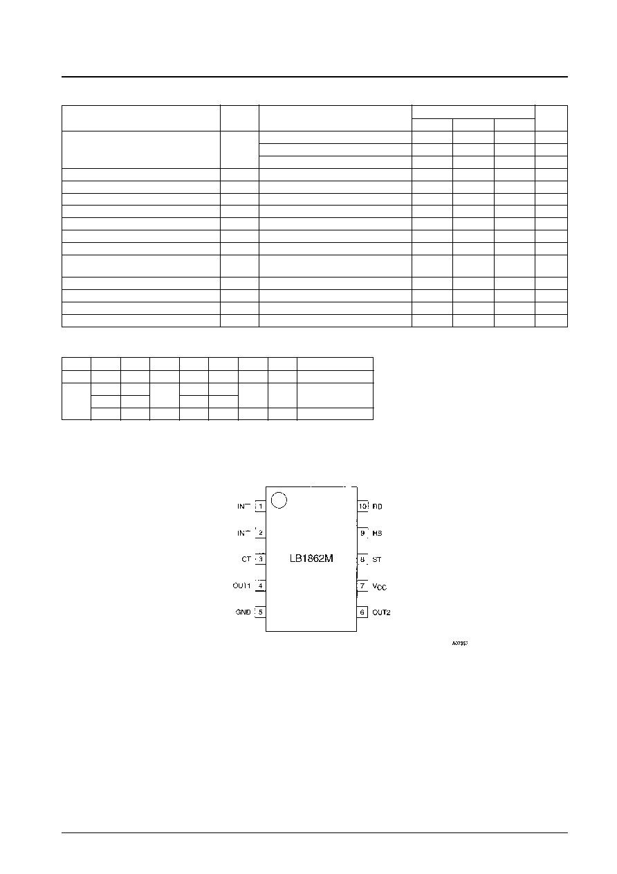
Package Dimensions
unit: mm
3086A-MFP10S
Monolithic Digital IC
Ordering number : EN5657
73097HA(OT) No. 5657-1/6
SANYO: MFP10S
SANYO Electric Co.,Ltd. Semiconductor Bussiness Headquarters
TOKYO OFFICE Tokyo Bldg., 1-10, 1 Chome, Ueno, Taito-ku, TOKYO, 110 JAPAN
Single-Phase Full-Wave Driver for Fan Motors
LB1862M
Parameter
Symbol
Conditions
Ratings
Unit
Supply voltage
V
CC
max
17
V
Output current
I
OUT
max
0.5
A
Output voltage
V
OUT
max
15
V
RD output voltage
V
R
max
15
V
RD output current
I
R
max
5
mA
HB output current
I
B
max
10
mA
ST input voltage
V
ST
max
15
V
Allowable power dissipation
Pd max
When mounted on the specified board
*
850
mW
Operating temperature
Topr
≠20 to +75
∞C
Storage temperature
Tstg
≠55 to +150
∞C
Specifications
Absolute Maximum Ratings
at Ta = 25∞C
Note:
*
Specified board: 114.3
◊
76.2
◊
1.5 mm epoxy glass laminate board
Parameter
Symbol
Conditions
Ratings
Unit
Supply voltage
V
CC
3.8 to 16.8
V
ST input high-level voltage
ST
H
3 to 14
V
ST input low-level voltage
ST
L
≠0.3 to +0.4
V
Hall input
V
ICM
0.2 to V
CC
≠1.5
V
common-mode input voltage range
Allowable Operating Ranges
at Ta = 25∞C
[LB1862M]
No. 5657-2/6
LB1862M
Parameter
Symbol
Conditions
Ratings
Unit
min
typ
max
During drive operation (CT = low, ST = low)
6.5
9.1
mA
Current drain
I
CC
During lock protection (CT = high, ST = low)
2.2
3.1
mA
Standby mode (ST = high)
110
150
µA
Lock detection capacitor charge current
I
CT
1
1.9
2.8
3.7
µA
Capacitor discharge current
I
CT
2
0.32
0.46
0.60
µA
Capacitor charge/discharge current ratio
R
CT
R
CD
= I
CT
1/I
CT
2
5.0
6.0
7.0
CT charge voltage
V
CT
1
2.55
2.75
2.95
V
CT discharge voltage
V
CT
2
1.6
1.8
2.0
V
Output low-level voltage
V
OL
I
O
= 200 mA
0.2
0.3
V
Output high-level voltage
V
OH
I
O
= 200 mA
3.9
4.1
V
Hall input sensitivity
V
HN
Zero peak value
7
15
mV
(Including the offset and hysteresis.)
RD output pin low-level voltage
V
RD
I
RD
= 5 mA
0.1
0.3
V
RD output pin leakage current
I
RDL
V
RD
= 15 V
30
µA
HB output low-level voltage
V
HBL
I
HB
= 5 mA
1.0
1.3
V
ST pin input current
I
ST
V
ST
= 5 V
75
100
µA
Electrical Characteristics
at Ta = 25∞C, V
CC
= 5 V
Truth Table
Pin Assignment
The RD output is a latch-type output; Low: drive, High: stopped
ST
IN
≠
IN
+
CT
OUT1
OUT2
RD
HB
Mode
H
--
--
--
off
off
off
off
Standby
H
L
L
H
L
L
L
Drive
L
L
H
L
H
H
off
off
off
L
Lock protection
Top view
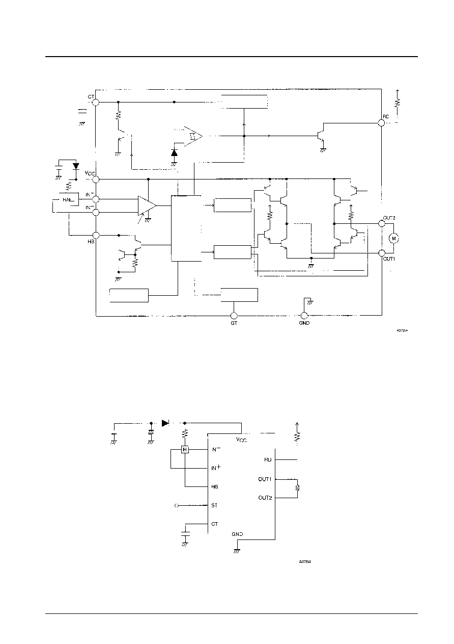
Block Diagram
Sample Application Circuit
No. 5657-3/6
LB1862M
0.47 to 1 µF
0.47 to 1 µF
Delay circuit
Delay circuit
Start/stop
Discharge
pulse
Charge/discharge
circuit
Amplifier with hysteresis
Thermal shutdown
circuit
Control
circuit

Startup
Lock Protection/Automatic Recovery
No. 5657-4/6
LB1862M
Power applied
Start/Stop
Lock
Output off
Output off
Output off
Output on
Lock cleared

Design Notes
1. V
CC
pin
This pin provides power for motor drive and the control circuits.
The LB1862M supports a wide range of operating voltages, from 3.8 to 16.8 V, and thus can be used in applications
that support both 5-V and 12-V systems.
2. OUT1 and OUT2 pins
Single-phase coil outputs.
The output is a high side inverted, low side single bipolar output. Since a regeneration circuit is included on chip, the
kickback current is regenerated across the low side NPN output even if a diode is used to protect the circuit against
being destroyed by reversed polarity connection.
3. IN
≠
and IN
+
pins
Hall element inputs.
The Hall signal is amplified to be a square wave by the Hall amplifier, which has hysteresis characteristics.
A hysteresis of ±3.5 mV (typical) is applied. A Hall input signal amplitude of 70 mV or higher is recommended.
4. CT pin
The capacitor connected between this pin and ground forms a protection circuit that prevents coil burnout if the motor
locks.
If the motor load returns to an appropriate level, the automatic recovery circuit will restart motor rotation. The lock
detection time can be set by changing the value of the capacitor.
If a 0.47 µF capacitor is used:
Lock detection time:
About 0.5 second
Lock protection time/automatic recovery time: About 0.16 second (output on)
About 1 second (output off)
This pin should be tied to ground if the lock protection function is not used.
5. RD pin
This is an open collector output that is low while the motor is turning and high impedance when the locked state is
detected.
This is a latch type output that holds the output high-impedance state if motor rotation is not restarted by the
automatic recovery circuit.
6. ST and HB pins
ST pin: Stops motor drive when a high level is input.
When ST is high, the RD pin output will go to the high-impedance state indicating lock protection mode.
HB pin: Switches the Hall bias. When a high level is input to the ST pin, applications should switch the Hall bias to
suppress standby mode current drain.
Both these pins should be left open if unused.
7. Thermal shutdown circuit
This circuit protects the IC by limiting the output current if the IC internal temperature reaches Tj = 180∞C.
No. 5657-5/6
LB1862M

No. 5657-6/6
LB1862M
This catalog provides information as of July, 1997. Specifications and information herein are subject to change
without notice.
s
No products described or contained herein are intended for use in surgical implants, life-support systems, aerospace
equipment, nuclear power control systems, vehicles, disaster/crime-prevention equipment and the like, the failure of
which may directly or indirectly cause injury, death or property loss.
s
Anyone purchasing any products described or contained herein for an above-mentioned use shall:
Accept full responsibility and indemnify and defend SANYO ELECTRIC CO., LTD., its affiliates, subsidiaries and
distributors and all their officers and employees, jointly and severally, against any and all claims and litigation and all
damages, cost and expenses associated with such use:
Not impose any responsibility for any fault or negligence which may be cited in any such claim or litigation on
SANYO ELECTRIC CO., LTD., its affiliates, subsidiaries and distributors or any of their officers and employees
jointly or severally.
s
Information (including circuit diagrams and circuit parameters) herein is for example only; it is not guaranteed for
volume production. SANYO believes information herein is accurate and reliable, but no guarantees are made or implied
regarding its use or any infringements of intellectual property rights or other rights of third parties.
Allowable power dissipation, Pdmax ≠ mW
Low side saturation output voltage,
V
O
(sat)L ≠ V
High side saturation output voltage,
V
O
(sat)H ≠ V
V
RD
, V
HB
≠ V
Input current, I
IN
≠
µ
A
Current drain, I
CC
≠ mA
Ambient temperature, Ta ≠ ∞C
Output current, I
O
-- mA
Output current, I
O
≠ mA
I
RD
, I
HB
≠ mA
Supply voltage, V
ST
≠ V
Supply voltage, V
CC
≠ V
V
RD
, V
HB
≠ I
RD
, I
HB
HB