 | –≠–ª–µ–∫—Ç—Ä–æ–Ω–Ω—ã–π –∫–æ–º–ø–æ–Ω–µ–Ω—Ç: LB1896 | –°–∫–∞—á–∞—Ç—å:  PDF PDF  ZIP ZIP |
3-phase Brushless Motor Driver for
CD-ROM Spindle Drive Use
Overview
The LB1896 is a 3-phase brushless motor driver IC that is
ideal for driving CD-ROM spindle motors.
Functions and Features
v 120 ∞ voltage linear technique
v V-type control voltage
v Switchable control gain
v Control, noncontrol, acceleration/deceleration mode select
pins built in.
v Start/Stop pin built in, Hall bias built in.
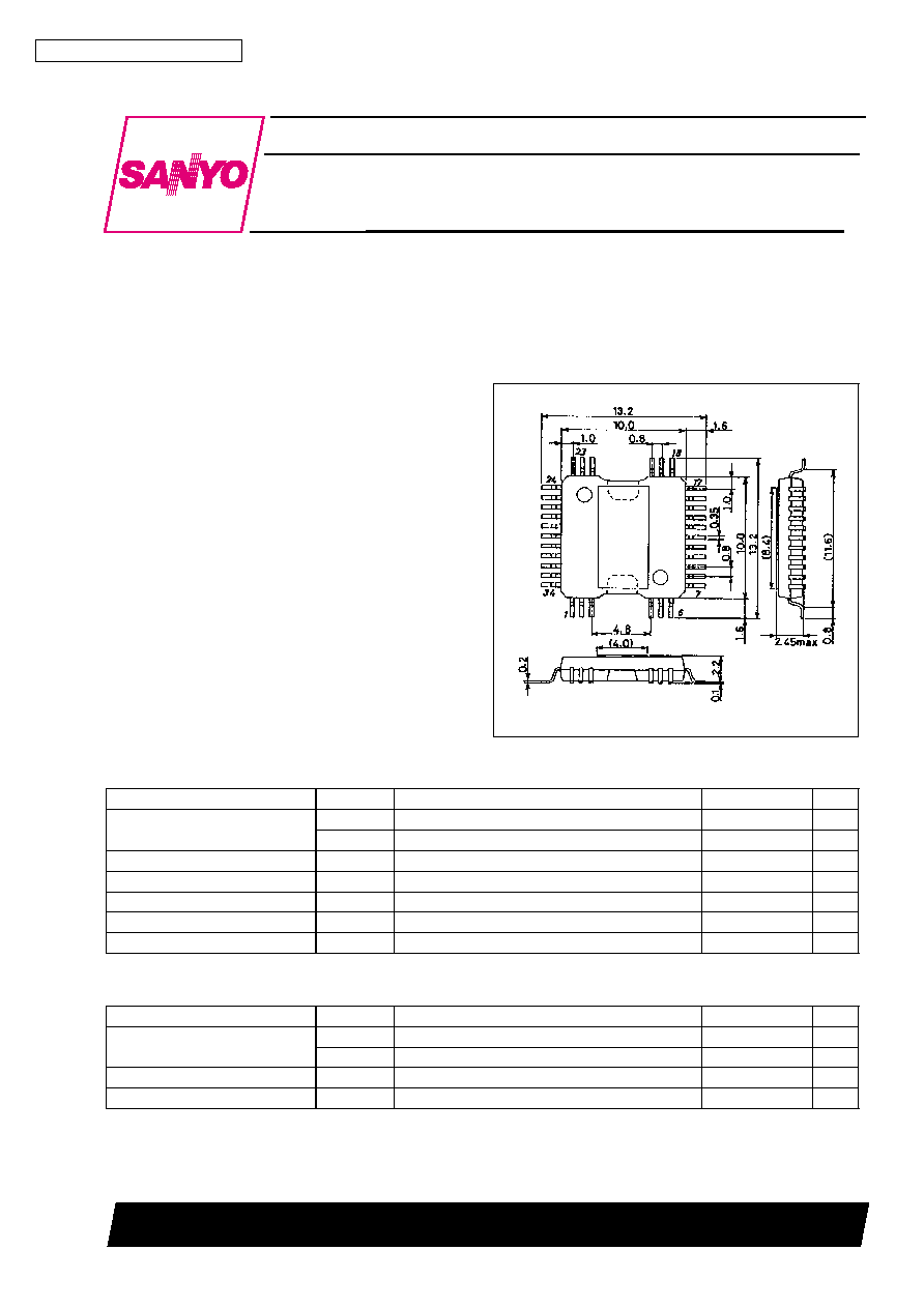
Package Dimensions
unit : mm
3219-QFP34H-C
[LB1896]
SANYO : QFP34H ≠ C
Specifications
Absolute Maximum Ratings
at Ta = 25 ∞C
Parameter
Symbol
Conditions
Ratings
Unit
Maximum supply voltage
V
CC
1 max
20
V
V
CC
2 max
7.0
V
Applied output voltage
V
OU, V, W
20
V
Output current
I
OUT
1.2
A
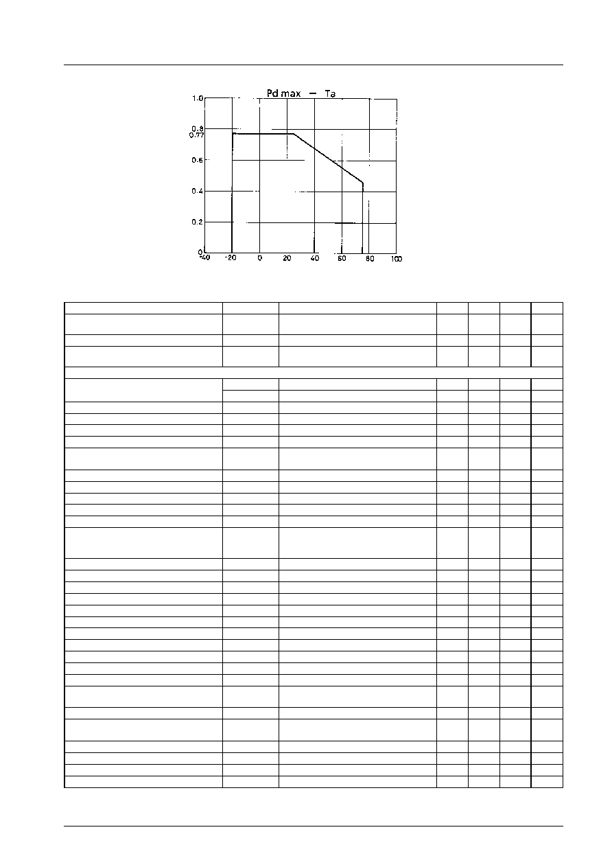
Allowable power dissipation
Pd max
Independent IC
0.77
W
Operating temperature
Topr
≠20 to +75
∞C
Storage temperature
Tstg
≠55 to +150
∞C
Operating Conditions
at Ta = 25 ∞C
Parameter
Symbol
Conditions
Ratings
Unit
Supply voltage
V
CC
1
5 to 18
V
V
CC
2
V
CC
1
^
V
CC
2
4.3 to 6.5
V
V
Cref
input voltage
V
Cref
V
CC
2/2
±
1.0
V
V
NS
input voltage
V
NS
0 to V
CC
2 ≠1.0
V
Ordering number: EN5225
Monolithic Digital IC
LB1896
SANYO Electric Co.,Ltd. Semiconductor Bussiness Headquarters
TOKYO OFFICE Tokyo Bldg., 1-10, 1 Chome, Ueno, Taito-ku, TOKYO, 110 JAPAN
13096HA(II) No.5225-1/8
Electrical Characteristics
at Ta = 25 ∞C, V
CC
1 = 12 V, V
CC
2 = 5 V
Parameter
Symbol
Conditions
min
typ
max
Unit
Supply current 1
I
CC
1
V
C
= open, V
Cref
= open, R
L
=
,
V
S/S
= 5 V
17
30
mA
Supply current 2
I
CC
2
V
C
= open, V
Cref
= open
7.5
10.5
mA
Supply current 3
I
CC
3
V
C
= open, V
Cref
= open, R
L
=
,
V
S/S
= 0 V, (I
CC
of V
CC
1)
0.9
3
mA
[Drive block]
Output saturation voltage
V
O(sat)
1
I
OUT
= 0.4 A, sink + source
1.6
2.2
V
V
O(sat)
2
I
OUT
= 0.8 A, sink + source
2.0
3.0
V
Output TRS sustaining voltage
V
O(sus)
I
OUT
= 20 mA
20
V
Output static voltage
V
OQ
V
C
= 2.5 V, V
Cref
= 2.5 V
5.7
6.0
6.3
V
Hall amplifier input offset voltage
V
H offset
≠5
+5
mV
Hall amplifier input bias current
I
H bias
1
5
µA
Hall amplifier common-mode input
voltage range
V
Hch
1.3
2.2
V
Hall input/output voltage gain
G
VHO
40
43
46
dB
Control/output drive gain 1
G
VCO
1
RZ1 = RZ2, GC1 = L, GC2 = L
26
29
dB
Control/output channel difference 1
G
VCO
1
RZ1 = RZ2, GC1 = L, GC2 = L
≠1.5
+1.5
dB
Control/output drive gain 2
G
VCO
2
RZ1 = RZ2, GC1 = L, GC2 = H
32
35
dB
Control/output channel difference 2
G
VCO
2
RZ1 = RZ2, GC1 = L, GC2 = H
≠1.9
+1.9
dB
Input dead zone voltage
V
DZ
RZ1 = RZ2, GC1 = L, GC2 = L
V
O
(voltage between out and out) =
0.1 V
±
13
±
38
±
55
mV
Input bias current 1
I
B SERVO
V
C
= 1.0 V
500
nA
Input bias current 2
I
B n.s
V
NS
= 1.0 V
500
nA
S/S pin high voltage
V
S/S H
Input is CMOS level
4
V
S/S pin low voltage
V
S/S L
Note) S/S pin Vth = V
CC
2/2
1
V
Gain control 1 high voltage
V
GC1 H
Input is at CMOS level.
4
V
Gain control 1 low voltage
V
GC1 L
Note) GC1 pin Vth = 2.0 V
1
V
Gain control 2 high voltage
V
GC2 H
Input is at CMOS level.
4
V
Gain control 2 low voltage
V
GC2 L
Note) GC2 pin Vth = 2.0 V
1
V
S/S pin input current
I
S/S
Input voltage = 5 V
50
100
µA
Gain control 1, 2 current
I
GC
Input voltage = 5 V
53
110
µA
Rotation output saturation voltage
V
(sat) H.FG
I
O
= ≠5 mA
0.24
0.5
V
Rotation output saturation sustaining
voltage
V
(sus) H.FG
7
V
Hall bias voltage
V
H
±
I
O
= 5 mA, R
H
= 200
0.7
0.97
1.2
V
CTRL pin high voltage
V
CTRL H
Common for CTRL1 and CTRL2
input CMOS level
4
V
CTRL pin low voltage
V
CTRL L
Note) CTRL pin Vth = 2.5 V
1.0
V
CTRL input current
I
CTRL
Input voltage = 5 V
53
110
µA
TSD operation voltage
TSD
Design target
150
180
210
∞C
TSD hysteresis
TSD
Design target
15
∞C
Note) Vth is a design target and not measured.
Allowable
power
dissipation,
Pd
max
--
W
Ambient temperature, Ta -- ∞C
LB1896
No.5225-2/8
Mode Switching Truth Table
CTRL0
CTRL1
Mode
L
L
Control
L
H
Noncontrol
H
L
Acceleration
H
H
Deceleration
L
= 0 to 1.0 V
H
= 4.0 V or more
Hall Logic Truth Table
Source
Sink
Hall input
F/R Control
U
IN
V
IN
W
IN
1
W
V
V
W
H
H
L
Forward
Reverse
2
W
U
U
W
H
L
L
Forward
Reverse
3
V
W
W
V
L
L
H
Forward
Reverse
4
U
V
V
U
L
H
L
Forward
Reverse
5
V
U
U
V
H
L
H
Forward
Reverse
6
U
W
W
U
L
H
H
Forward
Reverse
An input is considered to be HIGH when U
IN
1
>
U
IN
2, V
IN
1
>
V
IN
2, and W
IN
1
>
W
IN
2 by 0.2 V or more.
Forward when V
C
>
V
Cref
Reverse when V
C
<
V
Cref
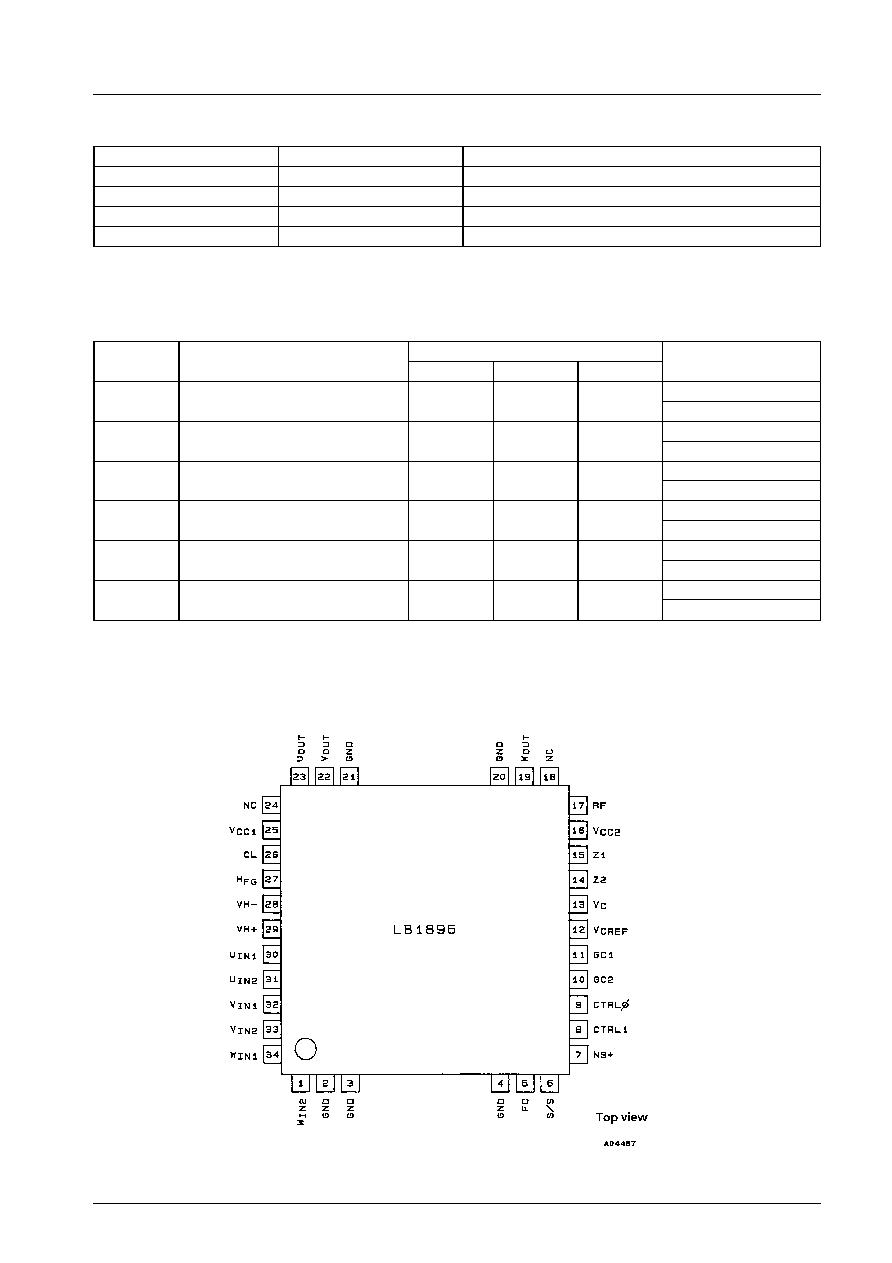
Pin Assignment
LB1896
No.5225-3/8

Pin Functions
Pin No.
Pin Name
Pin Voltage
Equivalent Circuit Diagram
Pin Function
3, 4
20, 21
Frame
GND
Frame GND.
GND must be shared.
2
GND
GND
23
22
19
U
OUT
V
OUT
W
OUT
Output pins.
Motor connection
17
Rf
Output Tr GND.
A resistor can be connected between this pin
and GND to sense the output current as a
voltage drop to provide for overcurrent
protection.
18, 24
NC
Idle pins.
16
V
CC
2
4.3 to 6.5 V
v
Power supply for blocks other than the
output block.
v
This supply should be kept stable to
prevent ripple and noise from entering this
pin.
15
14
Z1
Z2
v
First-stage amplifier gain setting resistors.
v
Z1 and Z2 normally range from several
tens of k
to several hundreds of k
.
v
The gain is about 6 dB.
13
12
V
C
V
Cref
V
CC
2/2
±
1.0
v
V
C
is the speed control pin.
Forward when V
C
>
V
Cref
.
Reverse when V
C
<
V
Cref
.
V
C
is used to control the output voltage.
v
V
Cref
determines the motor control stop
voltage.
V
CC
2/2 in normal use.
11
10
GC1
GC2
0 to V
CC
2
v
Input/output gain switching pins.
v
GC1 is for first-stage amplifier Z1/Z2
switching.
When GC1 is LOW, Z1 is selected;
when HIGH, Z2 is selected. GC2 is for
next-stage amplifier switching.
Continued on next page.
LB1896
No.5225-4/8
Continued from preceding page.
Pin No.
Pin Name
Pin Voltage
Equivalent Circuit Diagram
Pin Function
9
8
CTRL
CTRL1
0 to V
CC
2
v
Operation mode switching pins.
v
Refer to the Mode Switching Truth Table
for selection of control, acceleration, or
deceleration.
7
NS+
0 to
V
CC
2 - 1 V
v
Input pin at noncontrol mode.
v
The input-output gain is 14 dB.
(GC2: LOW)
v
Motor stops when V
NS
= 0 V.
6
S/S
0 to V
CC
2
v
When the S/S pin is HIGH, START;
when LOW, STOP.
v
The threshold is V
CC
2/2.
5
FC
v
Connect a capacitor between this pin and
GND to reduce the input/output gain
frequency response and to stop the
oscillator.
1
34
33
32
31
30
W
IN
2
W
IN
1
V
IN
2
V
IN
1
U
IN
2
U
IN
1
1.3 to 2.2 V
W-phase Hall device input pins.
Logic ``H'' represent W
IN
1
>
W
IN
2
V-phase Hall device input pins.
Logic ``H'' represent V
IN
1
>
V
IN
2
U-phase Hall device input pins.
Logic ``H'' represent U
IN
1
>
U
IN
2
Continued on next page.
LB1896
No.5225-5/8