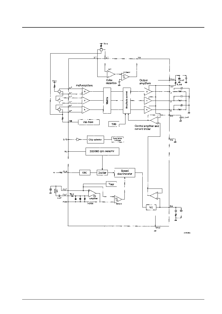
Overview
The LB1910 is a 3-phase disc drive motor driver that is
optimal for use as a 3.5-inch FDD spindle motor driver.
Functions and Features
∑ Three-phase full-wave linear driver
∑ Digital speed control circuit
∑ Start and stop circuits (active low)
∑ RPM switching
H: 300 rpm
L: 360 rpm
∑ Current limiter circuit
∑ Built-in index comparator
∑ Thermal shutdown circuit
Package Dimensions
unit: mm
3222-HSOP28
Monolithic Digital IC
43096HA (OT) No. 5383-1/7
SANYO: HSOP28
[LB1910]
SANYO Electric Co.,Ltd. Semiconductor Bussiness Headquarters
TOKYO OFFICE Tokyo Bldg., 1-10, 1 Chome, Ueno, Taito-ku, TOKYO, 110 JAPAN
FDD Spindle Motor Driver
LB1910
Ordering number : EN5383
Parameter
Symbol
Conditions
Ratings
Unit
Maximum supply voltage
V
CC
max
7.0
V
Maximum output current
I
O
max1
t
0.5 s
1.0
A
Maximum steady-state output current
I
O
max2
0.7
A
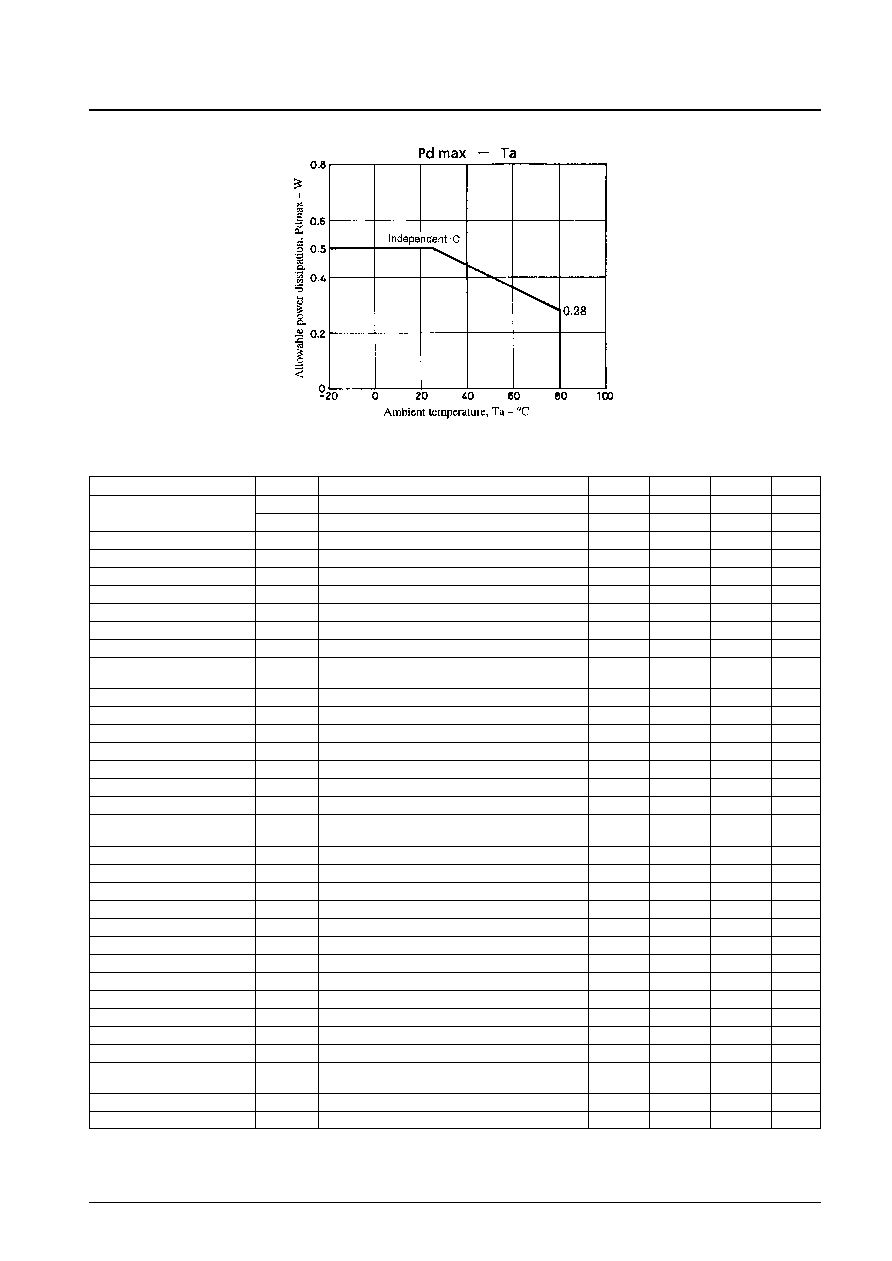
Allowable power dissipation
Pd max
Independent IC
0.5
W
Operating temperature
Topr
≠20 to +80
∞C
Storage temperature
Tstg
≠40 to +150
∞C
Specifications
Absolute Maximum Ratings
at Ta = 25∞C
Parameter
Symbol
Conditions
Ratings
Unit
Recommended supply voltage
V
CC
4.2 to 6.5
V
Allowable Operating Ranges
at Ta = 25∞C
No. 5383-2/7
LB1910
Electrical Characteristics
at Ta = 25∞C, V
CC
= 5 V
Parameter
Symbol
Conditions
min
typ
max
Unit
Current drain
I
CCO
S/S = 5 V (standby)
10
µA
I
CC
S/S = 0 V (steady state)
12
18
mA
SL bias current
I
SL
V
SL
= 0 V
10
µA
SL input low-level voltage
V
SLL
0
1.0
V
SL input high-level voltage
V
SLH
3.5
V
CC
V
S/S bias current
I
S/S
180
270
µA
S/S low-level voltage
V
S/SL
0
0.8
V
S/S high-level voltage
V
S/SH
3.5
V
CC
V
Hall amplifier input bias current
I
HB
10
µA
Common-mode input voltage
Vh
1.5
V
CC
≠ 1.0
V
range
Differential input voltage range
Vdif
50
200
mVp-p
Hall bias output voltage
V
H
I
H
= 5 mA
0.8
V
Leakage current
I
HL
S/S = 5 V
±10
µA
Output saturation voltage
Vsat
I
O
= 0.7 A, sink + source
1.3
1.8
V
Output leakage current
I
OL
1.0
mA
Current limiter
Vlim
0.27
0.3
0.33
V
Control amplifier voltage gain
G
C
≠7
dB
Voltage gain difference between
G
C
±1
dB
phases
V/I conversion source current
I
+
9
14
19
µA
V/I conversion sink current
I
≠
≠9
≠14
≠19
µA
V/I conversion current ratio
I
+
/I
≠
0.8
1.0
1.2
DSC buffer input current
I
DSC
1.0
µA
FG Schmitt hysteresis
Vsh
*
50
mV
Speed discriminator counts
N
1041.5
Discriminator operating frequency
F
D
*
1.1
MHz
Oscillator frequency range
F
OSC
*
1.1
MHz
Index output low-level voltage
V
IDL
I
O
= 2 mA
0.4
V
Index output leakage current
IIDL
±10
µA
FG amplifier voltage gain
G
FG
*
48
dB
FG amplifier input offset
V
FG O
±10
mV
FG amplifier internal reference
V
FG B
2.2
2.5
2.8
V
voltage
Thermal shutdown temperature
TSD
*
150
180
∞C
Hysteresis
TSD
*
40
∞C
Note:
*
Items marked with an asterisk are design target values and are not measured.

Pin Functions
No. 5383-5/7
LB1910
Pin No.
Symbol
Pin voltage
Equivalent circuit diagram
Function
Index output
L: 0.4 V max
H: 4.5 V min
ID
2
Index input
I
+
I
≠
28
1
∑ FG amplifier plus input
A 2.5-V reference voltage is generated
internally.
∑ FG amplifier minus input
∑ FG amplifier output
2.5 V
FG
IN
+
FG
IN
≠
FG
OUT
25
26
27
Minus side connection for providing the Hall bias
current
This pin becomes open in the stopped state, thus
cutting the Hall bias current.
0.8 V typ
(I
H
= 5 mA)
HB
24
U phase Hall element input
V phase Hall element input
W phase Hall element input
1.5 V min
V
CC
≠ 1.0 V
max
U
IN
+
U
IN
≠
V
IN
+
V
IN
≠
W
IN
+
W
IN
≠
18
19
20
21
22
23
Continued on next page.