 | –≠–ª–µ–∫—Ç—Ä–æ–Ω–Ω—ã–π –∫–æ–º–ø–æ–Ω–µ–Ω—Ç: LB1964T | –°–∫–∞—á–∞—Ç—å:  PDF PDF  ZIP ZIP |

LB1964T
No. 6188-1/4
Overview
The LB1964T is a driver for single-phase bipolar drive fan
motors that features compact and low-profile MSOP≠8
package. Low-saturation output and low-voltage operation
make it ideal for applications that require small size and
high efficiency, such as notebook computers and CPU
cooling fans.
Features
∑ Single-phase full-wave drive
∑ Low-voltage operation (V
CC
= 2.0V min.)
∑ Low-saturation output (upper side + lower side saturation
voltage: Vosat (total) = 0.3V typ., Io = 100 mA)
∑ Ultraminiature package (3.0
◊
4.9
◊
0.93 mm
3
)
∑ FG output
∑ Built-in thermal protection circuit
LB1964T
Package Dimensions
unit: mm
3245-MSOP8
O2599RM(KI)
Ordering number : ENN6188A
Monolithic Digital IC
Fan Motor Single-Phase Full-Wave Driver
[LB1964T]
SANYO : MSOP8
Specifications
Absolute Maximum Ratings
at Ta = 25∞C
Parameter
Symbol
Conditions
Ratings
Unit
Maximum supply voltage
V
CC
max
9
V
Allowable power dissipation
Pd max
With specified substrate*
370
mW
OUT output current
I
OUT
max
0.3
A
OUT output withstand voltage
V
OUT
max
9
V
FG output withstand voltage
V
FG
max
7
V
FG output current
I
FG
max
5
mA
Operating temperature
Topr
≠20 to +85
∞C
Storage temperature
Tstg
≠55 to +150
∞C
4.9
3.0
0.65
3.0
(0.5)
(0.85)
0.5
0.25
1
4
8
5
0.25
0.08
1.1max
Allowable Operating Ranges
at Ta = 25∞C
Parameter
Symbol
Conditions
Ratings
Unit
Power supply voltage
V
CC
2 to 8
V
Hall input common mode input voltage
V
ICM
0.2 to V
CC
≠1
V
range
Any and all SANYO products described or contained herein do not have specifications that can handle
applications that require extremely high levels of reliability, such as life-support systems, aircraft's
control systems, or other applications whose failure can be reasonably expected to result in serious
physical and/or material damage. Consult with your SANYO representative nearest you before using
any SANYO products described or contained herein in such applications.
SANYO assumes no responsibility for equipment failures that result from using products at values that
exceed, even momentarily, rated values (such as maximum ratings, operating condition ranges, or other
parameters) listed in products specifications of any and all SANYO products described or contained
herein.
SANYO Electric Co.,Ltd. Semiconductor Company
TOKYO OFFICE Tokyo Bldg., 1-10, 1 Chome, Ueno, Taito-ku, TOKYO, 110-8534 JAPAN
*
Specified substrate (20.0
◊
10.0
◊
0.8 mm
3
paper phenol)

LB1964T
No. 6188-2/4
Electrical Characteristics
at Ta = 25∞C, V
CC
= 3.3V, unless otherwise specified
Parameter
Symbol
Conditions
Ratings
Unit
min
typ
max
Current drain
Icc
3
4.5
mA
OUT output Low saturation voltage
V
OL
IO = 100 mA
0.2
0.3
V
OUT output High saturation voltage
V
OH
IO = 100 mA
0.2
0.3
V
Hall bias voltage
V
HB
RH = 360
1.17
1.27
1.37
V
Hall input sensitivity
V
HN
Zero peak value
1
7
mV
FG output Low voltage
V
FG
IFG = 3 mA
0.2
0.3
V
FG output leak current
I
FGL
VFG = 7V
30
µ
A
Thermal protection operating
TTSD
Assured design target*
150
180
200
∞C
temperature
* Assured design target: Target value, not measured individually
Truth Table
IN≠
IN+
OUT1
OUT2
FG
Mode
H
L
H
L
L
Rotating
L
H
L
H
Off
≠
≠
Off
Off
≠
In thermal protection
Pin Assignment
0.2
0.37
0.4
0
0.6
≠20
0
20
40
60
80
100
Allowable power dissipation, Pd max ≠ W
Pd max ≠ Ta
Ambient temperature, Ta ≠ ∞C
0.19
With specified substrate (20.0
◊
10.0
◊
0.8 mm3)
paper phenol
LB1964T
IN≠
IN+
HB
OUT1
GND
Top view
OUT2
FG
VCC
1
2
3
4
8
7
6
5

LB1964T
No. 6188-3/4
Sample Application Circuit
Block Diagram
GND
Thermal protection
circuit
M
FG
Control
circuit
HB
HALL
IN≠
IN+
VCC
OUT1
OUT2
Delay circuit
Constant voltage
circuit
Delay circuit
*1 When a diode is used to protect the IC from destruction in case of reverse connection, the capacitor Cr
must be inserted to provide a regenerative current route. Similarly, a capacitor is needed in the power
supply line, even if no diode is used.
*2 The Hall element is supplied with a constant-voltage bias of approx. 1.27V from the HB pin. This
ensures stable output with good temperature characteristics from the Hall element. Because the
LB1964T incorporates a Hall amplifier with low offset, it provides coil output with a stable duty.
*3 The Hall amplifier does not have a hysteresis characteristic. The OUT1 and IN≠ pins are at the same
phase, and by arranging the two pins next to each other, chatter during phase switching is prevented.
However, if the wiring leading to the IN≠ pin is long, some noise interference may occur. In such a
case, the following steps should be considered:
(1) Arrange parts layout with priority to proximity of Hall element and IC, to allow short Hall element
output wiring.
(2) Insert a resistor of about 10 to 100 k
between OUT1 and IN≠ to create a hysteresis characteristic.
GND
VCC
FG
OUT1
OUT2
IN+
IN≠
H
HB
1
Di
Cr
2
3
LB1964T
No. 6188-4/4
This catalog provides information as of October, 1999. Specifications and information herein are subject to change
without notice.
Specifications of any and all SANYO products described or contained herein stipulate the performance,
characteristics, and functions of the described products in the independent state, and are not guarantees
of the performance, characteristics, and functions of the described products as mounted in the customer's
products or equipment. To verify symptoms and states that cannot be evaluated in an independent device,
the customer should always evaluate and test devices mounted in the customer's products or equipment.
SANYO Electric Co., Ltd. strives to supply high-quality high-reliability products. However, any and all
semiconductor products fail with some probability. It is possible that these probabilistic failures could
give rise to accidents or events that could endanger human lives, that could give rise to smoke or fire,
or that could cause damage to other property. When designing equipment, adopt safety measures so
that these kinds of accidents or events cannot occur. Such measures include but are not limited to protective
circuits and error prevention circuits for safe design, redundant design, and structural design.
In the event that any or all SANYO products(including technical data,services) described or
contained herein are controlled under any of applicable local export control laws and regulations,
such products must not be exported without obtaining the export license from the authorities
concerned in accordance with the above law.
No part of this publication may be reproduced or transmitted in any form or by any means, electronic or
mechanical, including photocopying and recording, or any information storage or retrieval system,
or otherwise, without the prior written permission of SANYO Electric Co. , Ltd.
Any and all information described or contained herein are subject to change without notice due to
product/technology improvement, etc. When designing equipment, refer to the "Delivery Specification"
for the SANYO product that you intend to use.
Information (including circuit diagrams and circuit parameters) herein is for example only ; it is not
guaranteed for volume production. SANYO believes information herein is accurate and reliable, but
no guarantees are made or implied regarding its use or any infringements of intellectual property rights
or other rights of third parties.
PS
0.2
0
0.4
0.6
0.8
1.0
0
100
200
300
400
0.4
0.2
0
0.8
0.6
1.2
1.0
1.6
1.4
2.0
1.8
0
1
2
3
4
5
6
7
8
9
10
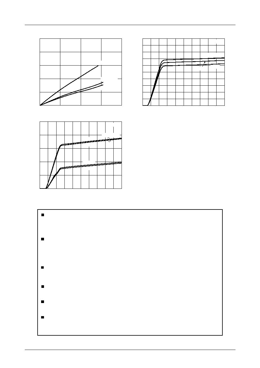
2
0
4
6
8
10
0
2
3
1
4
5
6
7
8
9
10
Upper + lower side
Lower side
Upper side
Hall bias voltage, HB ≠ V
RH = 560
RH = 360
IN+ = L
IN+ = L
IN≠ = L
IN≠ = L
360
240
Current drain, I
CC
≠ mA
Output saturation voltage, V
O
(sat) ≠V
ICC ≠ VCC
VO(sat) ≠ IO
HB ≠ VCC
Power supply voltage, VCC ≠ V
Output current, IO ≠ mA
VCC = 3V
Power supply voltage, VCC ≠ V
Tc = 25∞C
Ta = 25∞C