 | –≠–ª–µ–∫—Ç—Ä–æ–Ω–Ω—ã–π –∫–æ–º–ø–æ–Ω–µ–Ω—Ç: LB1971V | –°–∫–∞—á–∞—Ç—å:  PDF PDF  ZIP ZIP |
Ordering number :ENN6214A
91099RM (OT) No. 6214-1/9
Overview
The LB1971V is a bipolar sensorless motor driver that
provides a reverse torque braking function and is
appropriate for use as the spindle motor driver in CD and
MD players. Since the LB1971V can drive motors without
the use of Hall elements, this device can contribute to
miniaturization, thinner form factors, and lower power
dissipation in end products.
Functions and Features
∑ Three-phase bipolar sensorless drive
∑ Soft switching drive technique
∑ Reverse torque braking
∑ Standby mode power saving function
∑ FG outputs
∑ Can be operated from a 3-V supply.
∑ Thermal protection circuit
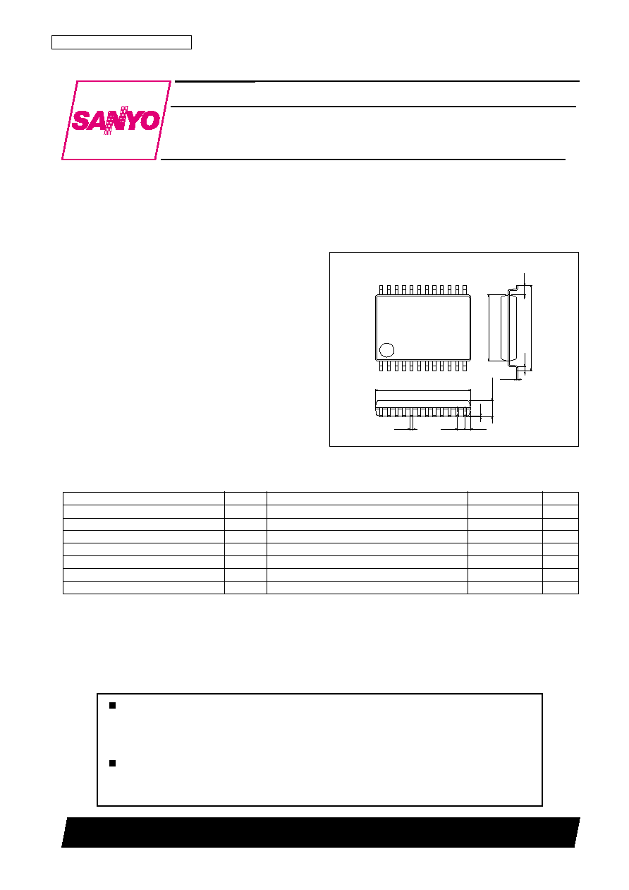
Package Dimensions
unit: mm
3175A-SSOP24
1
12
13
7.6
8.0
0.5
5.6
0.1
1.6max
1.0
24
0.65
0.22
0.43
0.15
SANYO: SSOP24
[LB1971V]
SANYO Electric Co.,Ltd. Semiconductor Company
TOKYO OFFICE Tokyo Bldg., 1-10, 1 Chome, Ueno, Taito-ku, TOKYO, 110-8534 JAPAN
Monolithic Digital IC
LB1971V
Three-Phase Full-Wave Sensorless CD
and MD Players Spindle Motor Driver
Any and all SANYO products described or contained herein do not have specifications that can handle
applications that require extremely high levels of reliability, such as life-support systems, aircraft's
control systems, or other applications whose failure can be reasonably expected to result in serious
physical and/or material damage. Consult with your SANYO representative nearest you before using
any SANYO products described or contained herein in such applications.
SANYO assumes no responsibility for equipment failures that result from using products at values that
exceed, even momentarily, rated values (such as maximum ratings, operating condition ranges, or other
parameters) listed in products specifications of any and all SANYO products described or contained
herein.
Parameter
Symbol
Conditions
Ratings
Unit
Maximum supply voltage 1
V
CC
1max
7.0
V
Maximum supply voltage 2
V
CC
2max
7.0
V
Maximum output circuit supply voltage
V
S max
7.0
V
Maximum output current
I
O max
700
mA
Allowable power dissipation
Pdmax
0.4
W
Operating temperature
Topr
≠20 to +75
∞C
Storage temperature
Tstg
≠55 to +150
∞C
Specifications
Absolute Maximum Ratings
at Ta = 25∞C
No. 6214-2/9
LB1971V
Electrical Characteristics
at V
CC
= 3.0 V, V
S
= 1.5 V, Ta = 25∞C
Parameter
Symbol
Conditions
Ratings
Unit
Supply voltage 1
V
CC
1
2.0 to 6.0
V
Supply voltage 2
V
CC
2
2.0 to 6.0
V
Output circuit supply voltage
V
S
0 to V
CC
2
V
FG pin applied voltage
V
FG
0 to 6.0
V
FG pin output current
I
FG
2.0
mA
Allowable Operating Ranges
at Ta = 25∞C
Parameter
Symbol
Conditions
Ratings
Unit
min
typ
max
[Current Drain]
Power save mode current drain
I
CC
1-1
STBY mode
5
µA
Operating current drain
I
CC
1-2
I
O
= 20 mA
3.6
4.6
mA
Pre-drive current
I
CC
2
I
O
= 20 mA
0.4
1.0
mA
Current drain + pre-drive current
I
CC
1+2
I
O
= 20 mA
4.0
5.5
mA
[Output Saturation Voltage]
Source 1-1
V
sat
1-1
I
O
= 0.4 A, V
CC
1 = V
CC
2 = V
S
0.90
1.00
V
Source 1-2
V
sat
1-2
I
O
= 0.2 A, V
CC
1 = V
CC
2 = V
S
0.85
0.95
V
Source 2-1
V
sat
2-1
I
O
= 0.4 A, V
CC
1 = V
CC
2 =3V, V
S
= 1.5 V
0.25
0.35
V
Source 2-2
V
sat
2-2
I
O
= 0.2 A, V
CC
1 = V
CC
2 =3V, V
S
= 1.5 V
0.15
0.25
V
Sink 1
V
sat
3-1
I
O
= 0.4 A
0.20
0.35
V
Sink 2
V
sat
3-2
I
O
= 0.2 A
0.13
0.25
V
[STBY Pin]
High-level input voltage
V
SSH
1.4
V
CC
1
V
Low-level input voltage
V
SSL
≠0.1
0.3
V
High-level input current
I
SSH
V
STBY
= 3.0 V
75
µA
Low-level input current
I
SSL
V
STBY
= 0 V
≠10
µA
[BRAKE Pin]
High-level input voltage
V
BRKH
1.4
V
CC
1
V
Low-level input voltage
V
BRKL
≠0.1
0.3
V
High-level input current
I
BRKH
V
BRK
= 3 V
60
µA
Low-level input current
I
BRKL
V
BRK
= 0 V
≠10
µA
[Startup Oscillator]
High-level output voltage
V
OSCH
1.35
1.50
1.65
V
Low-level output voltage
V
OSCL
0.50
0.65
0.80
V
[Position Detection Circuit]
Offset voltage
V
OFS
Design target value
≠10
+10
mV
Common-mode input voltage range
V
ICM
0
V
CC
2 ≠ 1.5
V
[FG Output Pin]
Output saturation voltage
V
FGSAT
IFG = 0.4 mA
0.1
0.25
V
[Thermal Protection Circuit]
Operating temperature
TSD
Design target value
150
180
∞C
Hysteresis
TSD
Design target value
40
∞C
[CX Oscillator]
High-level output voltage
V
CXH
0.8
1.0
1.2
V
Low-level output voltage
V
CXL
0.3
0.5
0.7
V
Oscillator frequency
f
CX
C = 470 pF
40
Hz
[SLOPE Circuit]
Charge current
I
CHG
1
≠6.0
≠4.5
≠3.0
µA
Discharge current
I
CHG
2
3.0
4.5
6.0
µA
No. 6214-3/9
LB1971V
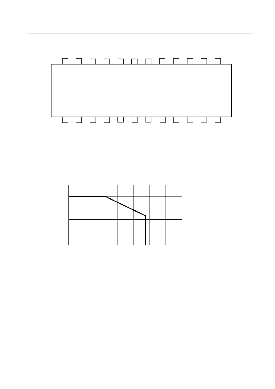
Pin Assignment
LB1971V
1
2
3
4
5
6
7
8
9
10
11
12
CSLP1
DET
FC
FG
VCC2
VS
VCC1
BRK
STBY
VOUT
UOUT
CSLP2
20
21
22
23
13
14
15
16
17
18
19
24
WOUT
NC
FCOM
UIN
CX
OSC
VIN
NC
NC
WIN
GND
RF
0. 5
0. 2
0. 4
0. 3
0. 1
0
120
100
80
60
40
20
0
-20
0. 24
Top view
Pd max -- Ta
Allowable power dissipation, Pdmax -- W
Ambient temperature, Ta -- ∞C

No. 6214-4/9
LB1971V
Application Circuit Example 1
: Portable CD Player (maximum speed: about 1000 rpm)
LB1971V
1
2
3
4
5
6
7
8
9
10
11
12
CSLP1
DET
FC
FG
VCC2
VS
VCC1
BRK
STBY
VOUT
UOUT
CSLP2
20
21
22
23
13
14
15
16
17
18
19
24
WOUT
NC
FCOM
UIN
CX
OSC
VIN
NC
NC
WIN
GND
RF
STBY
BRK
+
+
VS
1
µ
47
µ
0.047
µ
0.047
µ
0.47
µ
0.047
µ
470 p
4700 p
4700 p
4700 p
1.5 M
20 K
0.25
VCC
FG
Application Circuit Example 2
: Portable MD Player (maximum speed: about 2000 rpm)
LB1971V
1
2
3
4
5
6
7
8
9
10
11
12
CSLP1
DET
FC
FG
VCC2
VS
VCC1
BRK
STBY
VOUT
UOUT
CSLP2
20
21
22
23
13
14
15
16
17
18
19
24
WOUT
NC
FCOM
UIN
CX
OSC
VIN
NC
NC
WIN
GND
RF
STBY
BRK
+
+
VS
1
µ
47
µ
0.047
µ
0.022
µ
0.22
µ
0.022
µ
470 p
2200 p
2200 p
2200 p
1.5 M
20 K
0.25
VCC
FG
Unit (resistance:
, capacitance: F )
Unit (resistance:
, capacitance: F )

Notes on the LB1971V and External Components
1. Three-phase full-wave sensorless drive
The LB1971V is a 3-phase full-wave sensorless motor driver that provides a reverse torque braking function and is
appropriate for CD and MD players spindle motor drive. Furthermore, since this driver does not require the use of
Hall-effect devices, it can contribute to miniaturization, thinner form factors, and lower power in the motor system.
2. Power supply
This IC uses 3 power supply systems: V
S
, V
CC
1, and V
CC
2. V
S
is connected to the motor drive transistors, and allows
motor speed control to be implemented by connecting a power supply that varies according to the speed control.
Since V
CC
2 is connected to the pre-drive circuit and the position detection comparator circuit, the SOURCE pin
output can be made to have a low saturation voltage and a highly efficient motor operation can be achieved by
maintaining the condition that V
S
V
CC
2 ≠ 1 V. Also note that while this IC can be operated from voltages as low as
V
CC
1 = V
CC
2 = 2 V, the common-mode input voltage range of the position detector becomes quite narrow at this low
voltage, and care is required with respect to the applied V
S
voltage.
Capacitors with an adequate capacitance for stability must be inserted between each of the power supplies and
ground.
3. Soft switching drive
This IC adopts a soft switching drive technique to minimize motor noise. When the output transistors switch between
phases, a two-phase excitation state is created, and the output current is switched gradually to suppress motor noise.
The two-phase excitation state is determined by the amplitude of the CSLP pin waveform, and that waveform
amplitude is determined by the value of the capacitor connected at the CSLP pin and the motor speed. Note that while
the soft switching operation increases as the amplitude of the CSLP pin voltage decreases, drive efficiency is reduced
and timing problems may occur if this amplitude becomes too small. Therefore, the CSLP pin amplitude should be at
least 200 mVp-p at the maximum motor speed.
4. Position detection comparator circuit
The position detection comparator circuit uses the back EMF generated during motor rotation to detect the position of
the rotor. The position information acquired by this circuit is used to determine to which sections of the output block
power will be applied. Problems that occur during startup due to noise in the VS line can be prevented by inserting
capacitors between the FCOM pin and the UIN, VIN, and WIN pins. However, the timing with which power is
applied during high-speed motor operation may be delayed and efficiency reduced if these capacitors are too large.
5. Startup oscillator circuit (OSC pin)
This oscillator circuit creates the commutation logic timing required to start a sensorless motor.
A capacitor and a resistor are connected in parallel to ground. Use a high resistance of about 1.5 M
for this resistor.
The value of the capacitor depends on the characteristics of the motor: select a value such that the time required to
reach the target speed is minimum and the variation in the startup time is as small as possible. If the capacitance is too
large, the variations in startup time will increase, and if it is too small the motor may be prevented from starting up
normally.
6. CX oscillator circuit
This oscillator circuit creates the reference clock used for the sensorless motor logic system. Insert a capacitor to
ground. The oscillator frequency increases as the capacitance decreases. The oscillator frequency must be less than 60
Hz. (The recommended capacitance is 470 pF.)
7. FG output circuit
The FG output is created from the position detection information acquired from the back EMF waveform. This output
has a frequency three times that of the switching frequency. The output circuit is an open collector circuit. The output
is pulled up with a resistor.
No. 6214-5/9
LB1971V
No. 6214-6/9
LB1971V
Block Diagram
CX
UIN
VIN
WIN
SLOPE
TSD
GND
OSC
CX
FG
VCC1
VCC2
Rf
VS
V
W
U
BRK
FC
CSLP2
CSLP1
OSC
STBY
DET
U
V
W
BGP
BRK
STBY
+
+
+
PWM
FCOM
FCOM
Sensorless logic
Envelope detector
Output drive circuit
Soft switching drive
No. 6214-7/9
LB1971V
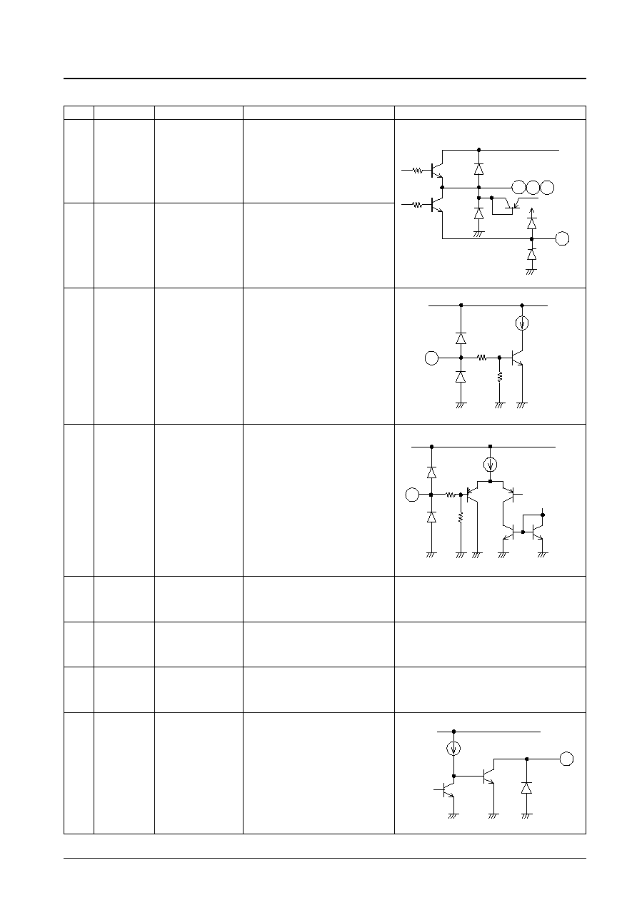
Pin Functions
Pin No.
Symbol
Pin voltage
Function
Equivalent circuit
2
1
23
U
OUT
V
OUT
W
OUT
V
CC
1
24
2
1 23
VS
Continued on next page.
∑ U, V, and W phases coil outputs
24
RF
∑ Rf connection
The LB1971V implements current control
using a resistor (Rf) connected between
this pin and ground to detect the drive
current.
0 to V
CC
1
3
STBY
V
CC
1
30 k
3
70 k
∑ Standby control
Normal operation: High
Standby: Low or open
0 to V
CC
1
4
BRK
V
CC
1
330
4
50 k
∑ Forward/reverse torque switching
Forward torque: Low or open
Reverse torque: High
2.0 V to 6.0 V
5
V
CC
1
∑ Power supply connection
6
8
V
S
FG
∑ FG output
These are open collector output.
V
CC
1
8
∑ Motor drive and speed control blocks
power supply
The voltage applied to this pin must be
strictly lower than V
CC
2.
0 V to V
CC
2
7
V
CC
2
2.0 V to 6.0 V
∑ Power supply connection for the pre-
drive circuit and the motor back EMF
detection comparator circuit

No. 6214-8/9
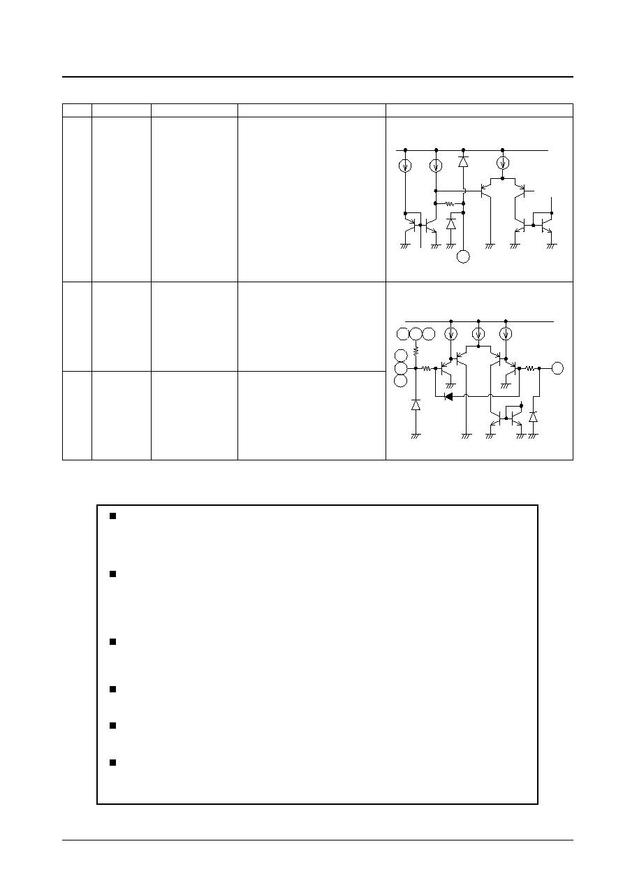
LB1971V
Pin No.
Symbol
Pin voltage
Function
Equivalent circuit
9
FC
Continued on next page.
10
DET
∑ Drive waveform sink side envelope
detection
Nothing connected to this pin in normal
operation.
11
12
CSLP1
CSLP2
V
CC
1
1 k
11 12
∑ Connection for the capacitor used for
triangular wave generation
The soft switching operation of the coil
output waveform is created using this
triangular waveform.
14
15
16
22
CX
NC
∑ Unused
∑ Clock oscillator used by the sensorless
logic
Connect a capacitor between the CX pin
and ground.
Oscillator frequency must be set up to
60 kHz.
Continued from preceding page.
∑ Frequency characteristics determination
Closed loop oscillation of the current
control system can be stopped by
connecting a capacitor between this pin
and ground.
1 k
V
CC
1
14
13
GND
∑Ground
V
CC
1
1 k
10
23
1
2
30 k
1 k
1 k
1 k
V
CC
1
9
2 k
PS No.6214-9/9
LB1971V
This catalog provides information as of September, 1999. Specifications and information herein are
subject to change without notice.
Specifications of any and all SANYO products described or contained herein stipulate the performance,
characteristics, and functions of the described products in the independent state, and are not guarantees
of the performance, characteristics, and functions of the described products as mounted in the customer's
products or equipment. To verify symptoms and states that cannot be evaluated in an independent device,
the customer should always evaluate and test devices mounted in the customer's products or equipment.
SANYO Electric Co., Ltd. strives to supply high-quality high-reliability products. However, any and all
semiconductor products fail with some probability. It is possible that these probabilistic failures could
give rise to accidents or events that could endanger human lives, that could give rise to smoke or fire,
or that could cause damage to other property. When designing equipment, adopt safety measures so
that these kinds of accidents or events cannot occur. Such measures include but are not limited to protective
circuits and error prevention circuits for safe design, redundant design, and structural design.
In the event that any or all SANYO products (including technical data, services) described or contained
herein are controlled under any of applicable local export control laws and regulations, such products must
not be exported without obtaining the export license from the authorities concerned in accordance with the
above law.
No part of this publication may be reproduced or transmitted in any form or by any means, electronic or
mechanical, including photocopying and recording, or any information storage or retrieval system,
or otherwise, without the prior written permission of SANYO Electric Co., Ltd.
Any and all information described or contained herein are subject to change without notice due to
product/technology improvement, etc. When designing equipment, refer to the "Delivery Specification"
for the SANYO product that you intend to use.
Information (including circuit diagrams and circuit parameters) herein is for example only; it is not
guaranteed for volume production. SANYO believes information herein is accurate and reliable, but
no guarantees are made or implied regarding its use or any infringements of intellectual property rights
or other rights of third parties.
Pin No.
Symbol
Pin voltage
Function
Equivalent circuit
17
OSC
18
20
19
W
IN
U
IN
V
IN
∑ Inputs to the motor back EMF detection
comparator
These pins are connected to the output
pins via a resistor internally in the IC.
Connect capacitors between these IN
pins and their corresponding -FCOM.
21
FCOM
∑ Motor coil midpoint input
The back EMF output is detected by
refering to these voltages.
Continued from preceding page.
∑ Connection for the triangular waveform
oscillator capacitor. This waveform is
used to generate the forcible motor
startup waveform during motor startup.
Connect a capacitor and a resistor
between this pin and ground.
Capacitance required depends on the
characteristics of motor.
Use a capacitor so that the time interval
until when the motor rotation reaches the
desired speed becomes the shortest.
1 k
V
CC
1
17
V
CC
1
19
18
20
21
200
200
10 k
1
2
23