Overview
The LC3564B, LC3564BS, LC3564BM, and LC3564BT
are 8192-word
◊
8-bit asynchronous silicon gate CMOS
SRAMs. These are full CMOS type SRAMs that adopt a
six-transistor memory cell and feature fast access times,
low operating power dissipation, and an ultralow standby
current. These SRAMs provide three control signal inputs:
an OE input for high-speed memory access, and two chip
enable lines, CE1 and CE2, for low power mode and
device selection. These means that these SRAMs area
ideal for systems that require low power and battery
backup, and that they support easy memory expansion.
The ultralow standby current that is a feature of these
SRAMs allows them to be used with capacitor backup as
well. Since these SRAMs support 3-V operation, they are
also appropriate for use in portable battery operated
systems.
Features
∑ Supply voltage range:
2.7 to 5.5 V
-- In 5-V operation mode: 5.0 V ±10%
-- In 3-V operation mode: 3.0 V ±10%
∑ Address access time (t
AA
)
-- In 5-V operation mode:
LC3564B, BS, BM, and BT-70: 70 ns (max)
LC3564B, BS, BM, and BT-10: 100 ns (max)
-- In 3-V operation mode:
LC3564B, BS, BM, and BT-70: 200 ns (max)
LC3564B, BS, BM, and BT-10: 500 ns (max)
∑ Ultralow standby current
-- In 5-V operation mode: 1.0 µA (Ta
70∞C),
3.0 µA (Ta
85∞C)
-- In 3-V operation mode: 0.8 µA (Ta
70∞C),
2.5 µA (Ta
85∞C)
∑ Operating temperature range
-- In 5-V operation mode: ≠40 to 85∞C
-- In 3-V operation mode: ≠40 to 85∞C
∑ Data retention supply voltage: 2.0 to 5.5 V
∑ All input and output levels:
-- In 5-V operation mode: TTL compatible levels
-- In 3-V operation mode: V
CC
≠0.2 V/0.2 V
∑ Three control inputs: OE, CE1, and CE2
∑ Shared input and output pins, three-state outputs
∑ No clock required
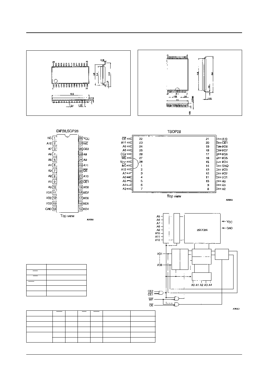
∑ Packages
28-pin DIP (600 mil) plastic package: LC3564B
28-pin DIP (300 mil) plastic package: LC3564BS
28-pin SOP (450 mil) plastic package: LC3564BM
28-pin TSOP (8
◊
13.4 mm) plastic package: LC3564BT
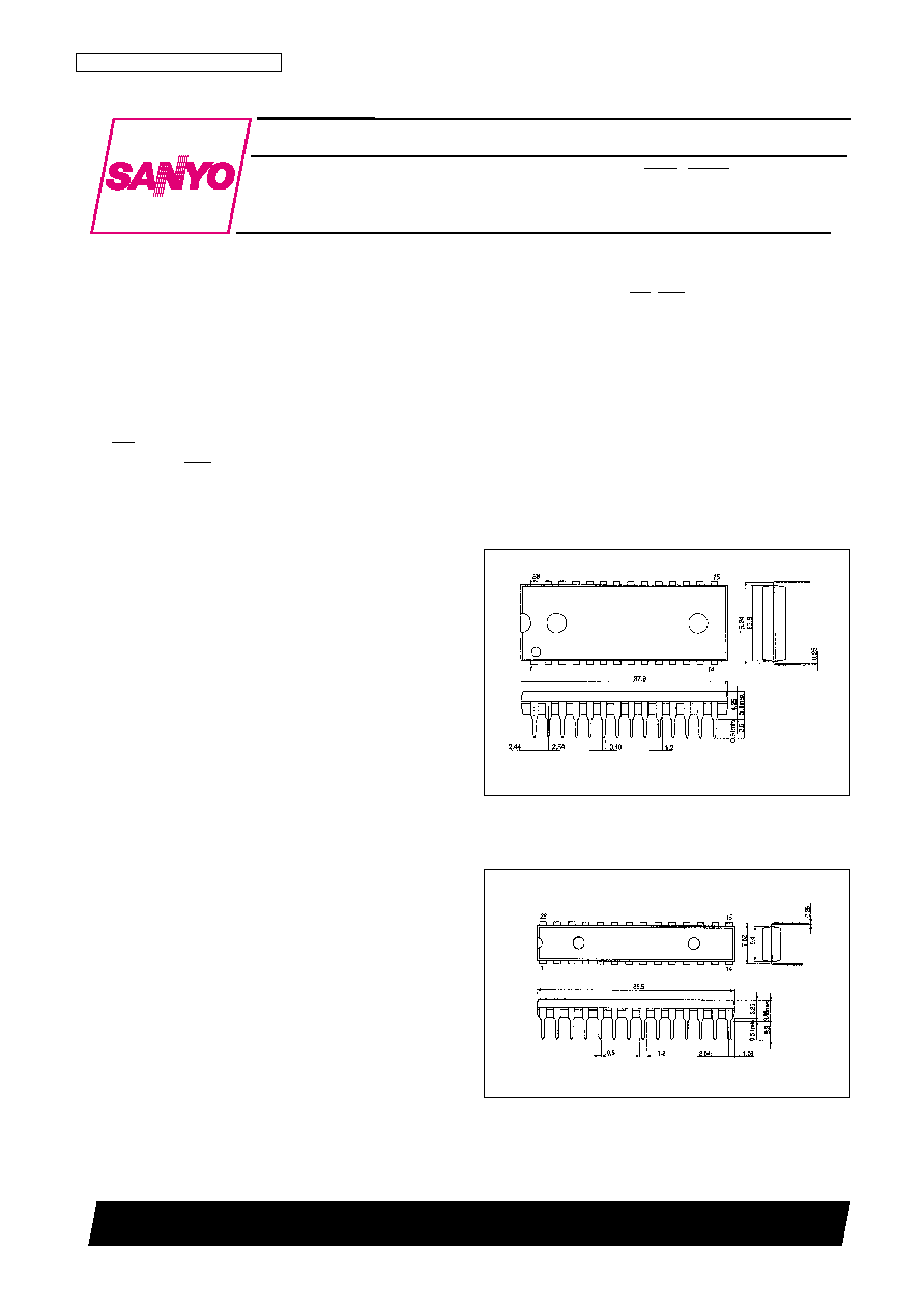
Package Dimensions
unit: mm
3012A-DIP28 (600 mil)
unit: mm
3133-DIP28 (300 mil)
CMOS IC
53098HA (OT) No. 5804-1/9
SANYO: DIP28 (600 mil)
[LC3564B]
SANYO: DIP28 (300 mil)
[LC3564BS]
SANYO Electric Co.,Ltd. Semiconductor Bussiness Headquarters
TOKYO OFFICE Tokyo Bldg., 1-10, 1 Chome, Ueno, Taito-ku, TOKYO, 110-8534 JAPAN
64K (8192-word
◊
8-bit) SRAM with OE, CE1, and CE2
Control Pins
LC3564B, BS, BM, BT-70/10
Ordering number : EN5804A
No. 5804-3/9
LC3564B, BS, BM, BT-70/10
Parameter
Symbol
Conditions
Ratings
Unit
Maximum supply voltage
V
CC
max
7.0
V
Input voltage
V
IN
≠0.3
*
to V
CC
+ 0.3
V
I/O voltage
V
I/O
≠0.3 to V
CC
+ 0.3
V
Operating temperature
Topr
≠40 to +85
∞C
Storage temperature
Tstg
≠55 to +125
∞C
Specifications
Absolute Maximum Ratings
at Ta = 25∞C
Note: For pulse widths less than 30 ns: ≠3.0 V
Note: These parameters are sampled, and are not measured for every unit.
Note: For pulse widths less than 30 ns: ≠3.0 V
Note
*
: Reference values at V
CC
= 5 V, Ta = 25∞C
[5-V Operation]
Parameter
Symbol
Conditions
Ratings
Unit
min
typ
max
I/O pin capacitance
C
I/O
V
I/O
= 0 V
6
10
pF
Input pin capacitance
C
IN
V
IN
= 0 V
6
10
pF
Input and Output Capacitances
at Ta = 25∞C, f = 1 MHz
Parameter
Symbol
Conditions
Ratings
Unit
min
typ
max
Supply voltage
V
CC
4.5
5.0
5.5
V
Input voltage
V
IH
2.2
V
CC
+ 0.3
V
V
IL
≠0.3
*
+0.8
V
DC Allowable Operating Ranges
at Ta = ≠40 to +85∞C, V
CC
= 4.5 to 5.5 V
Parameter
Symbol
Conditions
Ratings
Unit
min
typ
*
max
Input leakage current
I
LI
V
IN
= 0 to V
CC
≠1.0
+1.0
µA
I/O leakage current
I
LO
V
CE1
= V
IH
or V
CE2
= V
IL
or V
OE
= V
IH
or
≠1.0
+1.0
µA
V
WE
= V
IL
, V
I/O
= 0 to V
CC
Output high-level voltage
V
OH
I
OH
= ≠1.0 mA
2.4
V
Output low-level voltage
V
OL
I
OL
= 2.0 mA
0.4
V
V
CE1
0.2 V, V
CE2
V
CC
≠ 0.2 V, Ta
70∞C
0.01
1.0
µA
I
CCA1
I
I/O
= 0 mA, V
IN
0.2 V or
V
CC
≠ 0.2 V/0.2 V
V
IN
V
CC
≠ 0.2 V
Ta
85∞C
3.0
inputs
min
LC3564B,BS, BM, BT-70
35
mA
I
CCA4
cycle
LC3564B,BS,BM,BT-10
30
1 µs cycle
4
mA
Operating supply current
I
CCA2
V
CE1
= V
IL
, V
CE2
= V
IH
, I
I/O
= 0 mA,
7
mA
V
IN
= V
IH
or V
IL
TTL inputs
min
LC3564B,BS, BM, BT-70
40
mA
I
CCA3
cycle
LC3564B,BS,BM,BT-10
35
1 µs cycle
7
mA
Standby mode supply
V
CC
≠ 0.2 V/0.2 V
V
CE2
0.2 V or
Ta
70∞C
0.01
1.0
µA
current
inputs
I
CCS1
V
CE1
V
CC
≠ 0.2 V
V
CE2
V
CC
≠ 0.2 V
Ta
85∞C
3.0
TTL inputs
I
CC2
V
CE2
= V
IL
or V
CE1
= V
IH
, V
IN
= 0 to V
CC
2.0
mA
DC Electrical Characteristics
at Ta = ≠40 to +85∞C, V
CC
= 4.5 to 5.5 V
V
CE1
0.2 V,
V
CE2
V
CC
≠ 0.2 V,
I
I/O
= 0 mA,
DUTY = 100%
V
CE1
= V
IL
,
V
CE2
= V
IH
,
I
I/O
= 0 mA,
DUTY = 100%

AC Electrical Characteristics
at Ta = ≠40 to +85∞C, V
CC
= 4.5 to 5.5 V
No. 5804-4/9
LC3564B, BS, BM, BT-70/10
LC3564B, BS, BM, BT
Parameter
Symbol
-70
-10
Unit
min
max
min
max
Read cycle time
t
RC
70
100
ns
Address access time
t
AA
70
100
ns
CE1 access time
t
CA1
70
100
ns
CE2 access time
t
CA2
70
100
ns
OE access time
t
OA
35
50
ns
Output hold time
t
OH
10
10
ns
CE1 output enable time
t
COE1
10
10
ns
CE2 output enable time
t
COE2
10
10
ns
OE output enable time
t
OOE
5
5
ns
CE1 output disable time
t
COD1
30
35
ns
CE2 output disable time
t
COD2
30
35
ns
OE output disable time
t
OOD
25
25
ns
Read Cycle
LC3564B, BS, BM, BT
Parameter
Symbol
-70
-10
Unit
min
max
min
max
Write cycle time
t
WC
70
100
ns
Address setup time
t
AS
0
0
ns
Write pulse width
t
WP
50
55
ns
CE1 setup time
t
CW1
60
65
ns
CE2 setup time
t
CW2
60
65
ns
Write recovery time
t
WR
0
0
ns
CE1 write recovery time
t
WR1
0
0
ns
CE2 write recovery time
t
WR2
0
0
ns
Data setup time
t
DS
35
40
ns
Data hold time
t
DH
0
0
ns
CE1 data hold time
t
DH1
0
0
ns
CE2 data hold time
t
DH2
0
0
ns
WE output enable time
t
WOE
5
5
ns
WE output disable time
t
WOD
30
35
ns
Write Cycle
Parameter
Conditions
[AC Test Conditions]
Input pulse voltage
V
IH
= 2.4 V, V
IL
= 0.6 V
Input rise and fall times
5 ns
Input and output timing level
1.5 V
Output load
LC3564B, BS, BM, and BT-70: 30 pF + 1 TTL gate (Including the jig capacitance.)
LC3564B, BS, BM, and BT-10: 100 pF + 1 TTL gate (Including the jig capacitance.)