LC3564RM,RT-10LV/12LV/15LV
SANYO Electric Co., Ltd. Semiconductor Business Headquarters
TOKYO OFFICE Tokyo Bldg., 1-10, 1 Chome, Ueno, Taito-ku, TOKYO, 110 JAPAN
60597HA(ID) / 50995TH(ID) / D2293JN No. 4484--1/10
Ordering number: EN 4484B
CMOS LSI
64K (8192 words
◊
8 bits) SRAM
Overview
The LC3564RM,RT are 8192-word
◊
8bit, asynchronous,
silicon gate, low-voltage CMOS SRAM LSIs.They oper-
ate from a 2.0 to 3.6V supply, making them ideal for hand-
held, battery-operated equipment.
They are fully CMOS devices employing 2-layer A1 wir-
ing to realize high-speed access, low operating current
consumption and very low standby current. They incorpo-
rate control signal inputs; OE for high-speed memory
access, and 2 chip enables CE1 and CE2 for power-down
and device selection.
They are ideal for systems requiring high speed, low
power and battry backup or for easy mamory expansion.
The very low standby current means that backup can also
be achieved using a capacitor.
Features
s
Supply voltage range: 2.0 to 3.6V
∑ 3V operation: 2.7 to 3.6V
∑ Battery operation: 2.0 to 2.4V
s
High-speed access time
∑ 3V operation
- LC3564RM,RT-10LV: 100ns (max)
- LC3564RM,RT-12LV: 120ns (max)
- LC3564RM,RT-15LV: 150ns (max)
∑ Battery operation
- LC3564RM,RT-10LV: 200ns (max)
- LC3564RM,RT-12LV: 250ns (max)
- LC3564RM,RT-15LV: 300ns (max)
s
Very-low standby current
∑ 3V operation
- Ta
70
∞
C: 1.0
µ
A
- Ta
85
∞
C: 3.0
µ
A
∑ Battery operation
- Ta
70
∞
C: 0.85
µ
A
- Ta
85
∞
C: 2.5
µ
A
s
Operating temperature range: ≠40 to +85
∞
C
s
Data retention supply voltage: 2.0 to 3.6V
s
Input/output levels: CMOS Compatible (0.8Vcc/0.2Vcc)
s
3 control inputs (OE, CE1, CE2)
s
Common-pin input/outputs, 3-state output
s
Clock not needed (fully-static RAM)
s
Package
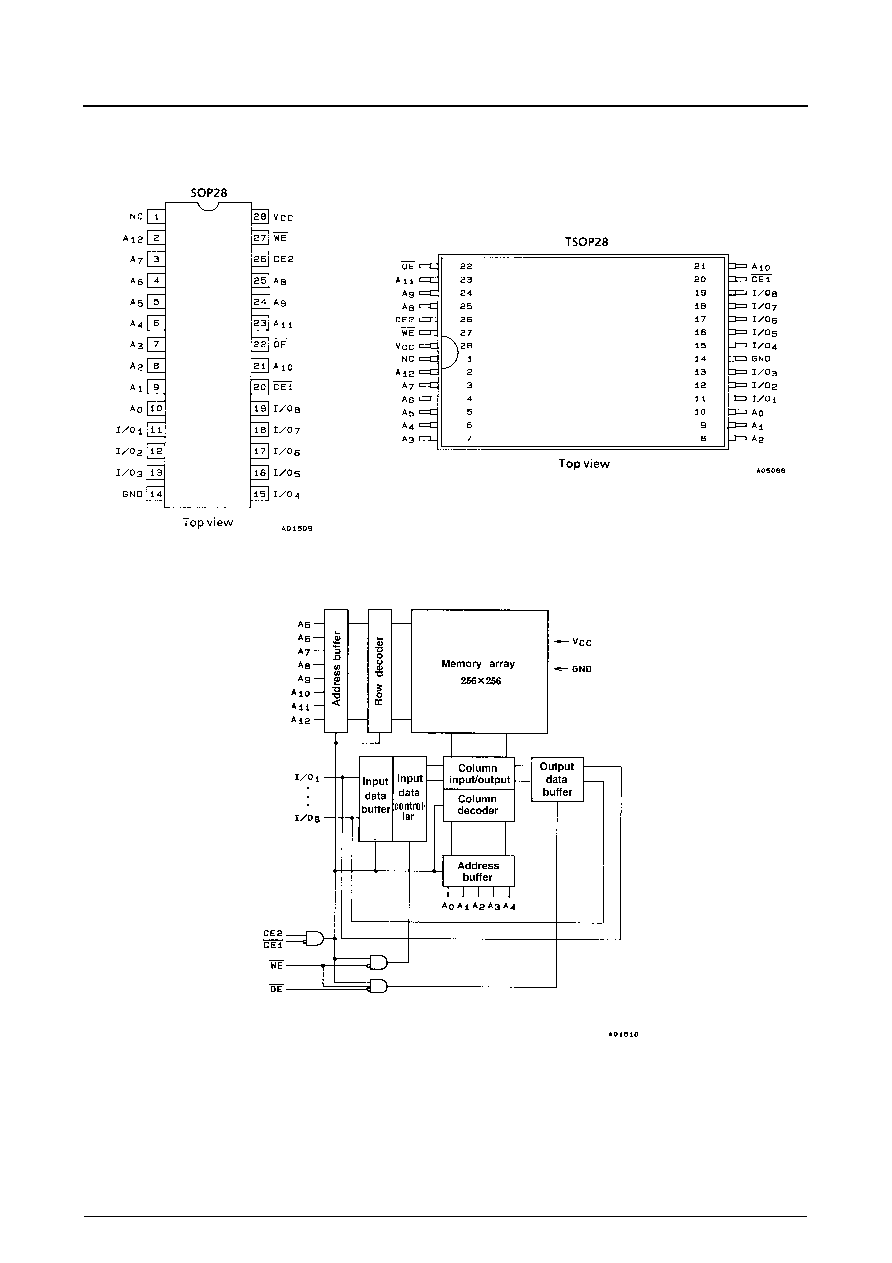
∑ SOP 28-pin (450mil) plastic package: LC3564RM
series
∑ TSOP 28-pin (8
◊
13.4mm) plastic package:
LC3564RT series
Package Dimensions
unit: mm
3158 - SOP28
unit: mm
3221 - TSOP28
[LC3564RM]
[LC3564RT]
LC3564RM,RT-10LV/12LV/15LV
No. 4484--3/10
Pin Functions
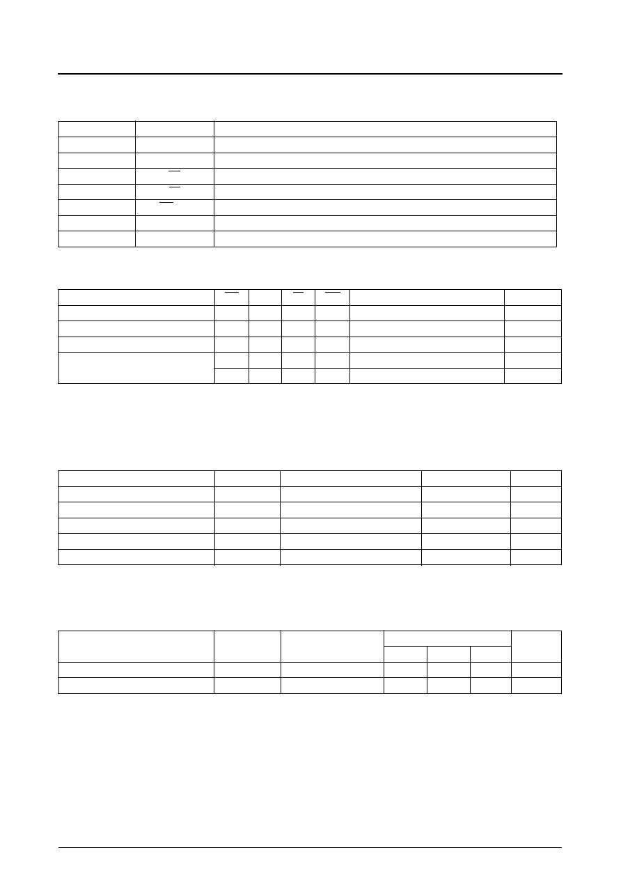
Truth Table
Note: X = H or L
Specifications
Absolute Maximum Ratings
at Ta = 25
∞
C
Note: Permanent device damage may occur if Absolute Maximum Ratings are exceeded. Functional operation should be restricted to Recommended operating condi-
tions. Exposure to higher than recommended voltages for extended periods of time could affect device reliability.
Inout/Output Capacitance
at Ta = 25
∞
C, f = 1 MHz
Note: Measured samples only.
Number
Name
Function
1
NC
No connection
2 to 10, 21, 23 to 25
A0 to A12
Address inputs
27
WE
Read/write control input
22
OE
Output enable input
20, 26
CE1, CE2
Chip enable inputs
11 to 13, 15 to 19
I/O1 to I/O8
Data input/outputs
28, 14
V
CC
, GND
Supply and ground pins
Mode
CE1
CE2
OE
WE1
I/O
Supply current
Read cycle
L
H
L
H
Data output
I
CCA
Write cycle
L
H
X
L
Data input
I
CCA
Output disable
L
H
H
H
High impedance
I
CCA
No selection
H
X
X
X
High impedance
I
CCS
X
L
X
X
High impedance
I
CCS
Parameter
Symbol
Conditions
Ratings
Unit
Maximum supply voltage
V
CC max
4.6
V
Input voltage range
V
IN
-
0.3 to V
CC
+ 0.3
V
Input/output voltage range
V
I/O
-
0.3 to V
CC
+ 0.3
V
Operating temperature range
T
opr
-
40 to +85
∞
C
Storage temperature range
T
stg
-
55 to +125
∞
C
Parameter
Symbol
Conditions
Ratings
Unit
min.
typ.
max.
Input/output pin capacitance
C
I/O
V
I/O
= 0V
-
6
10
pF
Input pin capacitance
C
I
V
I
= 0V
-
6
10
pF
LC3564RM,RT-10LV/12LV/15LV
No. 4484--4/10
3V Operation
DC Recommended Operating Ranges
at Ta = ≠40 to +85
∞
C, V
CC
= 2.7 to 3.6V
DC Electrical Characteristics
at Ta = ≠40 to +85
∞
C, V
CC
= 2.7 to 3.6V
* When pulsewidth is less than 30 ns, the minimum value is -2.0V.
* V
CC
= 3.0V, Ta = 25
∞
C
Parameter
Symbol
Ratings
Unit
min.
typ.
max.
Supply voltage
V
CC
2.7
3.0
3.6
V
Input voltage
V
IH
0.8V
CC
-
V
CC
+ 0.3
V
V
IL
-
0.3
*
-
0.2V
CC
V
Parameter
Symbol
Conditions
Ratings
Unit
min.
typ.
*
max.
Input leakage current
I
LI
V
IN
= 0V to V
CC
-
1.0
-
+1.0
µ
A
I/O leakage current
I
LO
V
CE1
= V
IH
or V
CE2
= V
IL
or
V
OE
= V
IH
or V
WE
= V
IL
,
V
I/O
= 0V to V
CC
-
1.0
-
+1.0
µ
A
Output high level voltage
V
OH
I
OH
=
-
2.0mA
V
CC
-
0.4
-
-
V
Output low level voltage
V
OL
I
OL
= 2.0mA
-
-
0.4
V
Operating supply
current
V
CC
≠
0.2V/0.2V input
I
CCA1
V
CE1
0.2V,
V
CE2
V
CC
≠ 0.2V,
I
I/O
= 0mA,
V
IN
0.2V or
V
IN
V
CC
≠ 0.2V
Ta
70
∞
C
-
0.01
1.0
µ
A
Ta
85
∞
C
-
-
3.0
µ
A
CMOS input
I
CCA2
V
CE1
= V
IL
, V
CE2
= V
IH,
I
I/O
= 0mA, V
IN
= V
IH
or V
IL
-
-
4
mA
I
CCA3
V
CE1
= V
IL
,
V
CE2
= V
IH,
I
I/O
= 0mA,
duty = 100%
min. cycle
-
-
25
mA
200 ns cycle
-
-
15
mA
1
µ
s cycle
-
-
10
mA
Standby supply
current
V
CC
-
0.2V/0.2V input
I
CCS1
V
CE2
0.2V or
{V
CE1
V
CC
-
0.2V,
V
CE2
V
CC
-
0.2V}
Ta
70
∞
C
-
0.01
1.0
µ
A
Ta
85
∞
C
-
-
3.0
µ
A
CMOS input
I
CCS2
V
CE2
= V
IL
or V
CE1
= V
IH
,
V
IN
= 0V to V
CC
-
-
1
mA
LC3564RM,RT-10LV/12LV/15LV
No. 4484--5/10
AC Electrical Characteristics
at Ta = ≠40 to +85
∞
C, V
CC
= 2.7 to 3.6V
AC test conditions
Input pulse voltage level: 0.2V
CC
to 0.8 V
CC
Input rise and fall times: 5 ns
Input/output timing level: V
CC
/2
Output load: 30 pF (including jig capacitance)
Read Cycle
Write Cycle
Parameter
Symbol
LC3564RM,RT
Unit
-10LV
-12LV
-15LV
min.
max.
min.
max.
min.
max.
Read cycle time
t
RC
100
-
120
-
150
-
ns
Address access time
t
AA
-
100
-
120
-
150
ns
CE1 access time
t
CA1
-
100
-
120
-
150
ns
CE2 access time
t
CA2
-
100
-
120
-
150
ns
OE access time
t
OA
-
50
-
60
-
75
ns
Output hold time
t
OH
10
-
10
-
10
-
ns
CE1 output enable time
t
COE1
10
-
10
-
10
-
ns
CE2 output enable time
t
COE2
10
-
10
-
10
-
ns
OE output enable time
t
OOE
5
-
5
-
5
-
ns
CE1 output disable time
t
COD1
-
35
-
40
-
50
ns
CE2 output disable time
t
COD2
-
35
-
40
-
50
ns
OE output disable time
t
OOD
-
25
-
30
-
40
ns
Parameter
Symbol
LC3564RM,RT
Unit
-10LV
-12LV
-15LV
min.
max.
min.
max.
min.
max.
Write cycle time
t
WC
100
-
120
-
150
-
ns
Address setup time
t
AS
0
-
0
-
0
-
ns
Write pulsewidth
t
WP
60
-
70
-
80
-
ns
CE1 setup time
t
CW1
70
-
80
-
90
-
ns
CE2 setup time
t
CW2
70
-
80
-
90
-
ns
Write recovery time
t
WR
0
-
0
-
0
-
ns
CE1 write recovery time
t
WR1
0
-
0
-
0
-
ns
CE2 write recovery time
t
WR2
0
-
0
-
0
-
ns
Data setup time
t
DS
50
-
55
-
60
-
ns
Data hold time
t
DH
0
-
0
-
0
-
ns
CE1 data hold time
t
DH1
0
-
0
-
0
-
ns
CE2 data hold time
t
DH2
0
-
0
-
0
-
ns
WE output enable time
t
WOE
5
-
5
-
5
-
ns
WE output disable time
t
WOD
-
35
-
40
-
45
ns