Ordering number : ENN6303
12800RM (OT) No. 6303-1/6
Overview
The LC35V256EM-70W and LC35V256ET-70W are
asynchronous silicon-gate CMOS SRAMs with a 32768-
word by 8-bit structure. These are full-CMOS devices
with 6 transistors per memory cell, and feature ultralow-
voltage operation, a low operating current drain, and an
ultralow standby current. Control inputs include OE for
fast memory access and CE for power saving and device
selection. This makes these devices optimal for systems
that require low power or battery backup, and makes
memory expansion easy. The ultralow standby current
allows these devices to be used with capacitor backup as
well.
Features
∑ Supply voltage range: 3.0 to 3.6 V
∑ Access time: 70 ns (maximum)
∑ Standby current: 0.8 µA (Ta
60∞C)
4.0 µA (Ta
70∞C)
∑ Operating temperature: ≠10 to +70∞C
∑ Data retention voltage: 2.0 to 3.6 V
∑ All I/O levels: CMOS compatible (0.8 V
CC
, 0.2 V
CC
)
∑ Input/output shared function pins, 3-state output pins
∑ No clock required (fully static circuits)
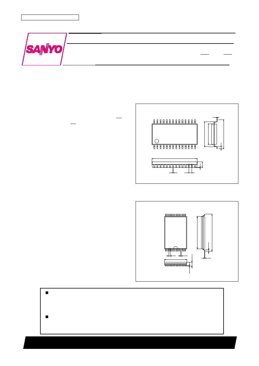
∑ Package
28-pin SOP (450 mil) plastic package:
LC35V256EM-70W
28-pin TSOP (8
◊
13.4 mm) plastic package:
LC35V256ET-70W
Package Dimensions
unit: mm
3187A-SOP28D
unit: mm
3221-TSOP28 (Type I)
LC35V256EM, ET-70W
SANYO Electric Co.,Ltd. Semiconductor Company
TOKYO OFFICE Tokyo Bldg., 1-10, 1 Chome, Ueno, Taito-ku, TOKYO, 110-8534 JAPAN
256K (32K words
◊
8 bits) SRAM
Control pins: OE and CE
CMOS IC
1
14
15
28
11.8
1.0
8.4
9.8
18.0
0.1 2.3
1.27
0.4
0.15
SANYO: SOP28D
[LC35V256EM-70W]
Any and all SANYO products described or contained herein do not have specifications that can handle
applications that require extremely high levels of reliability, such as life-support systems, aircraft's
control systems, or other applications whose failure can be reasonably expected to result in serious
physical and/or material damage. Consult with your SANYO representative nearest you before using
any SANYO products described or contained herein in such applications.
SANYO assumes no responsibility for equipment failures that result from using products at values that
exceed, even momentarily, rated values (such as maximum ratings, operating condition ranges, or other
parameters) listed in products specifications of any and all SANYO products described or contained
herein.
0.55
22
7
21
8
1
28
8.1
1.27max
11.8
13.4
0.5
0.2
0.125
0.08
SANYO: TSOP28 (Type I)
[LC35V256ET-70W]
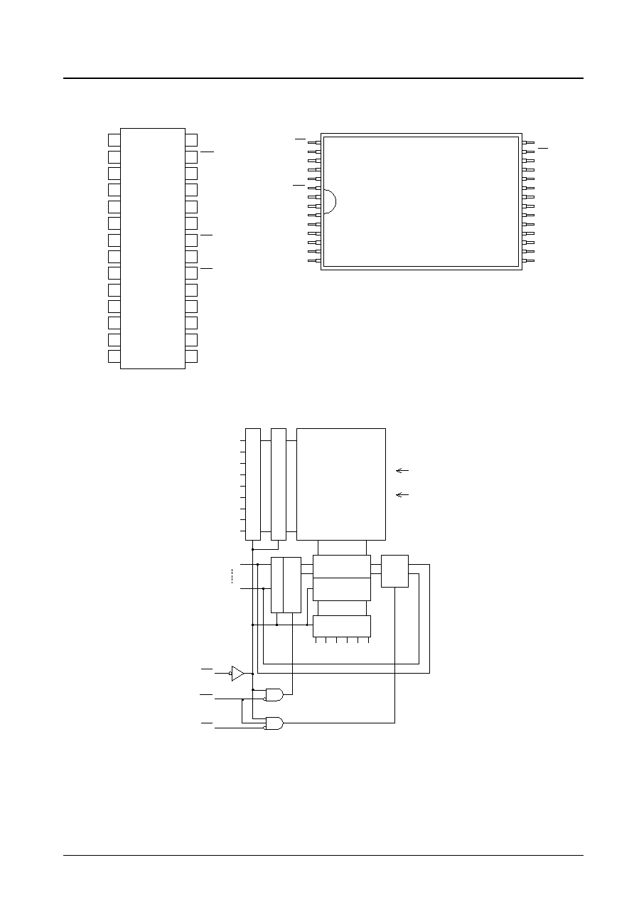
Pin Functions
No. 6303-3/6
LC35V256EM, ET70W
A0 to A14
Address input
WE
Read/write control input
OE
Output enable input
CE
Chip enable input
I/O1 to I/O8
Data I/O
V
CC
, GND
Power supply, ground
Function Table
Mode
CE
OE
WE
I/O
Supply current
Read cycle
L
L
H
Data output
I
CCA
Write cycle
L
X
L
Data input
I
CCA
Output disable
L
H
H
High impedance
I
CCA
Unselected
H
X
X
High impedance
I
CCS
Parameter
Symbol
Conditions
Ratings
Unit
Maximum supply voltage
V
CC
max
4.6
V
Input pin voltage
V
IN
≠0.3
*
to V
CC
+ 0.3
V
I/O pin voltage
V
I/O
≠0.3 to V
CC
+ 0.3
V
Operating temperature
Topr
≠10 to +70
∞C
Storage temperature
Tstg
≠55 to +125
∞C
Specifications
Absolute Maximum Ratings
Note:
*
The minimum value is ≠2.0 V for pulse widths under 30 ns.
I/O Capacitances
at Ta = 25∞C, f = 1 MHz
Parameter
Symbol
Conditions
Ratings
Unit
min
typ
max
I/O pin capacitance
C
I/O
V
I/O
= 0 V
6
10
pF
Input pin capacitance
C
I
V
IN
= 0 V
6
10
pF
Note: All units are not tested; only samples are tested.
DC Allowable Operating Ranges
at Ta = ≠10 to +70∞C, V
CC
= 3.0 to 3.6 V
Parameter
Symbol
Conditions
Ratings
Unit
min
typ
max
Supply voltage
V
CC
3.0
3.3
3.6
V
Input voltage
V
IH
0.8V
CC
V
CC
+ 0.3
V
V
IL
≠0.3
*
0.2V
CC
V
Note:
*
The minimum value is ≠2.0 V for pulse widths under 30 ns.
Note: X indicates H or L.
No. 6303-4/6
LC35V256EM, ET70W
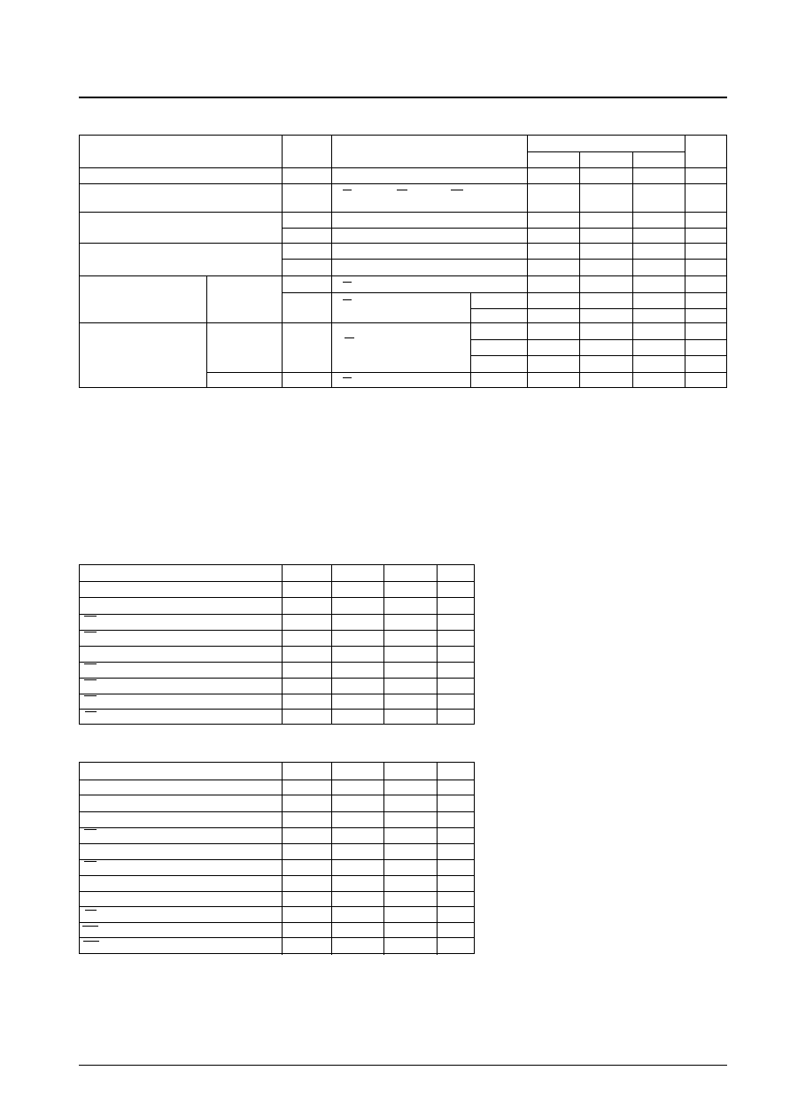
DC Electrical Characteristics
at Ta = ≠10 to +70∞C, V
CC
= 3.0 to 3.6 V
Parameter
Symbol
Conditions
Ratings
Unit
min
typ
max
Input leakage current
I
LI
V
IN
= 0 to V
CC
≠1.0
+1.0
µA
Output leakage current
I
LO
V
CE
= V
IH
or V
OE
= V
IH
or V
WE
= V
IL
≠1.0
+1.0
µA
V
I/O
= 0 to V
CC
Output high-level voltage
V
OH1
I
OH1
= ≠2.0 mA
V
CC
≠ 0.4
V
V
OH2
I
OH2
= ≠100 µA
V
CC
≠ 0.1
V
Output low-level voltage
V
OL1
I
OL1
= 2.0 mA
0.4
V
V
OL2
I
OL2
= 100 µA
0.4
V
I
CCA2
V
CE
= V
IL
, I
I/O
= 0 mA, V
IN
= V
IH
or V
IL
1.2
mA
Operating current drain
I
CCA3
V
CE
= V
IL
, V
IN
= V
IH
or V
IL
min cycle
20
25
mA
I
I/O
= 0 mA, DUTY 100 %
1 µs cycle
1.5
2.5
mA
Ta
25∞C
0.01
µA
Standby mode
I
CCS1
Ta
60∞C
0.8
µA
current drain
Ta
70∞C
4.0
µA
I
CCS2
V
CE
= V
IH
, V
IN
= 0 to V
CC
0.4
mA
Note:
*
Reference values when V
CC
= 3.3 V and Ta = 25∞C.
CMOS inputs
V
CE
V
CC
≠ 0.2 V,
V
IN
= 0 to V
CC
V
CC
≠ 0.2 V/
0.2 V inputs
CMOS inputs
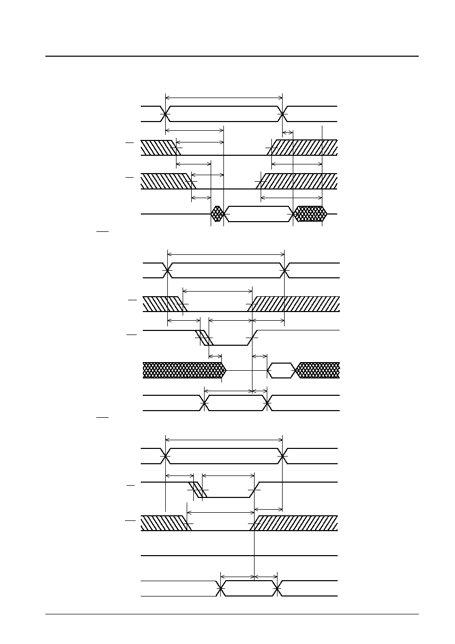
AC Electrical Characteristics
at Ta = ≠10 to +70∞C, V
CC
= 3.0 to 3.6 V
AC test conditions
Input pulse voltage levels: 0.2 V
CC
to 0.8 V
CC
Input rise and fall times: 5 ns
Input and output timing levels: 1/2 V
CC
Output load: 30 pF (including the jig capacitance)
Parameter
Symbol
min
max
Unit
Read cycle time
t
RC
70
ns
Address access time
t
AA
70
ns
CE access time
t
CA
70
ns
OE access time
t
OA
50
ns
Output hold time
t
OH
10
ns
CE output enable time
t
COE
10
ns
OE output enable time
t
OOE
5
ns
CE output disable time
t
COD
35
ns
OE output disable time
t
OOD
30
ns
Read Cycle
Parameter
Symbol
min
max
Unit
Write cycle time
t
WC
70
ns
Address setup time
t
AS
0
ns
Write pulse width
t
WP
55
ns
CE setup time
t
CW
60
ns
Write recovery time
t
WR
0
ns
CE write recovery time
t
WR1
0
ns
Data setup time
t
DS
50
ns
Data hold time
t
DH
0
ns
CE data hold time
t
DH1
0
ns
WE output enable time
t
WOE
5
ns
WE output disable time
t
WOD
35
ns
Write Cycle