Ordering number : EN4163A
22896HA (OT)/21593JN (OT) No. 4163-1/7
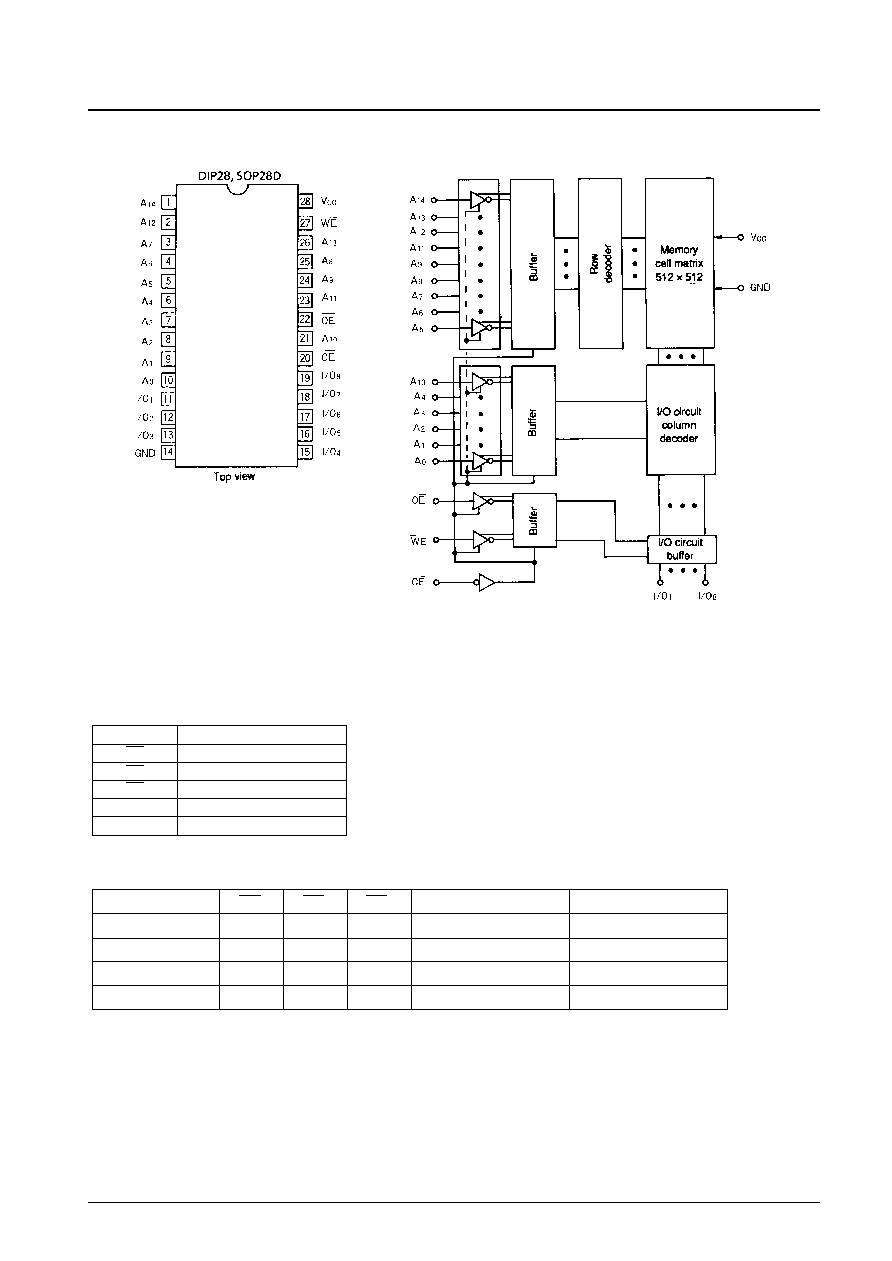
Overview
The LC36256AL, AML are fully asynchronous silicon
gate CMOS static RAMs with an 32768 words
◊
8 bits
configuration.
This series have CE chip enable pin for device
select/nonselect control and an OE output enable pin for
output control, and features high speed as well as low
power dissipation.
For these reasons, the series is especially suited for use in
systems requiring high speed, low power, and battery
backup, and it is easy to expand memory capacity.
Features
∑ Access time
70
ns (max.) : LC36256AL-70, LC36256AML-70
85
ns (max.) : LC36256AL-85, LC36256AML-85
100 ns (max.) : LC36256AL-10, LC36256AML-10
120 ns (max.) : LC36256AL-12, LC36256AML-12
∑ Low current dissipation
During standby
2
µA (max.) / Ta = 25∞C
5
µA (max.) / Ta = 0 to +40∞C
25 µA (max.) / Ta = 0 to +70∞C
During data retention
1
µA (max.) / Ta = 25∞C
2
µA (max.) / Ta = 0 to +40∞C
10 µA (max.) / Ta = 0 to +70∞C
During operation (DC)
10 mA (max.)
∑ Single 5 V power supply: 5 V ±10%
∑ Data retention power supply voltage: 2.0 to 5.5 V
∑ No clock required (Fully static memory)
∑ All input/output levels are TTL compatible
∑ Common input/output pins, with three output states
∑ Packages
DIP 28 -pin (600 mil) plastic package : LC36256AL
SOP 28-pin (450 mil) plastic package : LC36256AML
Package Dimensions
unit: mm
3012A - DIP28
unit : mm
3187 - SOP28D
SANYO: DIP28
[LC36256AL]
SANYO: SOP28D
[LC36256AML]
LC36256AL, AML-70/85/10/12
SANYO Electric Co.,Ltd. Semiconductor Bussiness Headquarters
TOKYO OFFICE Tokyo Bldg., 1-10, 1 Chome, Ueno, Taito-ku, TOKYO, 110-0005 JAPAN
256 K (32768 words
◊
8 bits) SRAM
Asynchronous Silicon Gate CMOS LSI
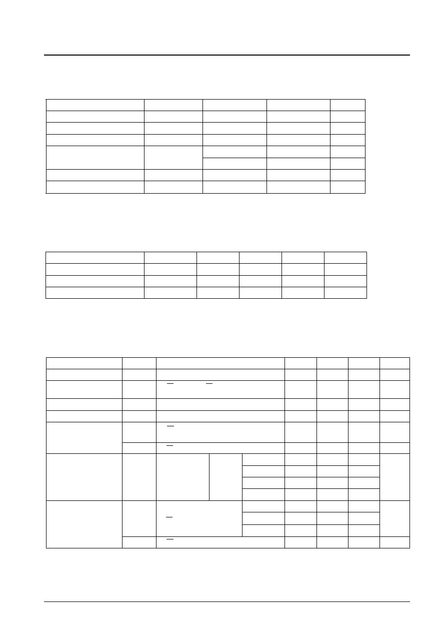
Specifications
Absolute Maximum Ratings
at Ta=25∞C
Parameter
Symbol
Conditions
Ratings
Unit
Maximum supply voltage
V
CC
max
7.0
V
Input pin voltage
V
IN
≠0.5
*
to V
CC
+0.5
V
I/O pin voltage
V
I/O
≠0.5
*
to V
CC
+0.5
V
Allowable power dissipation
Pd max
LC36256AL
1.0
W
LC36256AML
0.7
W
Operating temperature range
Topr
0 to +70
∞C
Storage temperature range
Tstg
≠55 to +150
∞C
* ≠3.0 V when pulse width is less than 50 ns
DC Recommended Operating Ranges
at Ta = 0 to +70∞C
Parameter
Symbol
min
typ
max
Unit
Power supply voltage
V
CC
4.5
*
5.0
5.5
V
Input high level voltage
V
IH
2.2
*
V
CC
+0.3
V
Input low level voltage
V
IL
≠0.3
*
+0.8
V
* ≠3.0 V when pulse width is less than 50 ns
DC Electrical Characteristics
at Ta = 0 to +70∞C, V
CC
= 5 V ±10%
Parameter
Symbol
Conditions
min
typ
*
max
Unit
Input leakage current
I
LI
V
IN
= 0 to V
CC
≠0.5
+0.5
µA
I/O leakage current
I
LO
V
CE
= V
IH
or V
OE
= V
IH,
≠0.5
+0.5
µA
V
I/O
= 0 to V
CC
Output high level voltage
V
OH
I
OH
= ≠1.0mA
2.4
V
Output low level voltage
V
OL
I
OL
= 2.1mA
0.4
V
Operating supply
I
CCA1
V
CE
0.2V,
1
5
mA
current (DC)
V
IN
0.2V or V
IN
V
CC
≠0.2V
I
CCA2
V
CE
= V
IL
, I
I/O
=0mA
3
10
mA
min cycle
70ns
30
50
Average operating
I
CCA3
Duty = 100%
85ns
25
50
mA
supply current
I
I/O
= 0mA
100ns
23
50
120ns
20
50
0 to +70∞C
25
Standby supply
I
CCS1
V
CE
V
CC
-0.2V
0 to +40∞C
5
µA
current
25∞C
0.5
2
I
CCS2
V
CE
= V
IH
0.4
2
mA
* Reference values at V
CC
= 5 V, Ta = 25∞C
LC36256AL, AML-70/85/10/12
No. 4163-3/7
Access
time
LC36256AL, AML-70/85/10/12
No. 4163-4/7
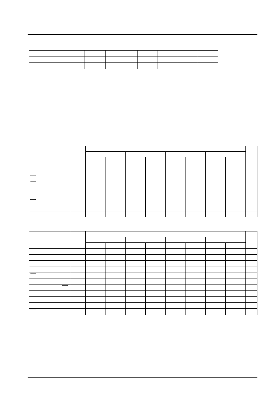
Input/Output Capacitance
at Ta = 25∞C, f = 1 MHz
Parameter
Symbol
Conditions
min
typ
max
Unit
Input/output capacitance
C
I/O
V
I/O
= 0V
8
pF
Input capacitance
C
IN
V
IN
= 0V
6
pF
Note:
These parameters were obtained through sampling, and not full-lot measurement.
AC Electrical Characteristics
at Ta = 0 to +70∞C, V
CC
= 5 V ±10%
AC testing conditions
Input pulse voltage level
:
0.8 V, 2.2 V
Input rise and fall time
:
5 ns
Input - output timing level
:
1.5 V
Output load
:
1 TTL gate + C
L
= 100 pF (85 ns/100 ns/120 ns)
1 TTL gate + C
L
= 30 pF (70 ns)
(including scope and jig capacitance)
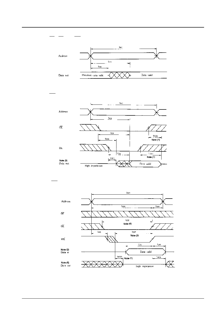
Read Cycle
Parameter
Symbol
LC36256AL, AML
-70
-85
-10
-12
Unit
min
max
min
max
min
max
min
max
Read cycle time
t
RC
70
85
100
120
ns
Address access time
t
AA
70
85
100
120
ns
CE access time
t
CA
70
85
100
120
ns
OE access time
t
OA
35
45
50
60
ns
Output hold time
t
OH
20
20
20
20
ns
CE output enable time
t
COE
10
10
10
10
ns
OE output enable time t
OOE
5
5
5
5
ns
OE output disable time t
COD
0
30
0
30
0
30
0
30
ns
OE output disable time t
OOD
0
30
0
30
0
30
0
30
ns
Write Cycle
LC36256AL, AML
Parameter
-70
-85
-10
-12
Unit
min
max
min
max
min
max
min
max
Write cycle time
t
WC
70
85
100
120
ns
Address valid to end of write t
AW
65
75
80
100
ns
Address setup time
t
AS
0
0
0
0
ns
Write pulse width
t
WP
50
50
60
70
ns
CE setup time
t
CW
65
75
80
100
ns
Write recovery time (WE) t
WR
0
0
0
0
ns
Write recovery time (CE) t
WR
1
0
0
0
0
ns
Data setup time
t
DS
30
30
35
40
ns
Data hold time
t
DH
0
0
0
0
ns
WE output enable time t
WOE
10
10
10
10
ns
WE output disable time t
WOD
0
25
0
25
0
25
0
25
ns