 | –≠–ª–µ–∫—Ç—Ä–æ–Ω–Ω—ã–π –∫–æ–º–ø–æ–Ω–µ–Ω—Ç: LC4100 | –°–∫–∞—á–∞—Ç—å:  PDF PDF  ZIP ZIP |
Overview
The LC4100C is a common driver for large-scale dot
matrix LCD panels. It includes a 240-bit bidirectional shift
register and 4-level LCD driver circuits. The number of
bits can be further increased by using the provided input
and output pins to connect multiple LC4100Cs in cascade.
The LC4100C and LC4101C form a large-screen LCD
panel driver chip set.
Features
∑ Fabricated in a CMOS (P-sub) high-voltage process.
∑ LCD drive voltage: 36 V
∑ Logic system power-supply voltage: 3.0 to 5.5 V
∑ f
load
max: 1 MHz
∑ Slim chip (output pads are concentrated on one of the
longer sides)
∑ 240 outputs (pad pitch: 70 µm)
∑ Bidirectional shift register
∑ The shift register can be split into two 120-bit registers.
∑ DISPOFF function that locks the drive voltages output
to the LCD at fixed levels.
∑ Display duty: 1/160 to 1/480
CMOS LSI
93096HA (OT)/31596HA (OT) No. 5279-1/8
SANYO Electric Co.,Ltd. Semiconductor Bussiness Headquarters
TOKYO OFFICE Tokyo Bldg., 1-10, 1 Chome, Ueno, Taito-ku, TOKYO, 110 JAPAN
LCD Dot Matrix Common Driver
for STN Displays
LC4100C
Ordering number : EN5279B
Parameter
Symbol
Conditions
Ratings
Unit
V
DD
≠0.3 to +7
V
Supply voltage
V
EEn
≠0.3 to +40
V
V
SSn
≠0.3 to +0.3
V
V
IN
LOAD, L/R, DISP, DF, EIO1, EIO3, EIO4
≠0.3 to V
DD
+ 0.3
V
Input voltage
V
0
, V
1
V
EE
≠ 7 to V
DD
+ 0.3
V
V
4
≠0.3 to V
SS
+ 7
V
V
5
≠0.3 to +0.3
V
Operating temperature
Topr
≠20 to +75
∞C
Storage temperature
Tstg
≠55 to +125
∞C
Specifications
Absolute Maximum Ratings
at Ta = 25∞C ± 2∞C, standard V
SS
, V
EEn
= V
EE1
or V
EE2
, V
SSn
= V
SS1
or V
SS2
Note: The voltages V
1
, V
2
, V
3
, V
4
, and V
5
must obey the relationships V
EEn
+ 0.3
V
0
V
1
V
EE
≠ 7, and 7
V
4
V
5
V
SSn
≠ 0.3. (Unit: V)
No. 5279-2/8
LC4100C
Parameter
Symbol
Conditions
Ratings
Unit
min
typ
max
V
DD
3.0
5.5
V
Supply voltage
V
EEn
20
36
V
V
SSn
0
V
Input high-level voltage
V
IH
LOAD, L/R, DISP, DF, EIO1, EIO3, EIO4
0.8 V
DD
V
DD
V
Input low-level voltage
V
IL
LOAD, L/R, DISP, DF, EIO1, EIO3, EIO4
0
0.2 V
DD
V
V
0
, V
1
V
0
, V
1
V
EEn
≠ 7
V
EEn
V
Input voltage
V
4
V
4
0
V
EEn
+ 7
V
V
5
V
5
0
V
Clock frequency
f
load
LOAD
1
MHz
V
DD
=
High-level clock
t
w (ldh)
LOAD
50
ns
5 V ± 10%
pulse width
EIO input setup time
t
su (ei)
LOAD, EIO1, EIO3, EIO4
100
ns
EIO input hold time
t
ho (ei)
LOAD, EIO1, EIO3, EIO4
30
ns
Clock frequency
f
load
LOAD
200
kHz
V
DD
=
High-level clock
t
w (ldh)
LOAD
120
ns
3 to 4.5 V
pulse width
EIO input setup time
t
su (ei)
LOAD, EIO1, EIO3, EIO4
120
ns
EIO input hold time
t
ho (ei)
LOAD, EIO1, EIO3, EIO4
40
ns
Allowable Operating Ranges
at Ta = ≠20 to +75∞C, standard V
SS
, V
EEn
= V
EE1
or V
EE2
, V
SSn
= V
SS1
or V
SS2
Parameter
Symbol
Conditions
Ratings
Unit
min
typ
max
Input high-level current
I
IH
V
IN
= V
DD
: LOAD, L/R, DISP, DF, EIO1, EIO3, EIO4
1
µA
Input low-level current
I
IL
V
IN
= V
SS
: LOAD, L/R, DISP, DF, EIO1, EIO3, EIO4
≠1
µA
Output high-level voltage
V
OH
I
O
= ≠0.4 mA: EIO1, EIO4
0.8 V
DD
V
DD
V
Output low-level voltage
V
OL
I
O
= 0.4 mA: EIO1, EIO4
V
SS
0.2 V
DD
V
V
EE1
, V
EE2
= 20 V, V
0
= 20 V, V
0
≠ V
0
= 0.5 V,
Output on resistance
R
OUT
V
1
= 20 V, V
1
≠ V
0
= 0.5 V, V
4
= 0 V, V
0
≠ V
4
= 0.5 V,
0.3
0.6
k
V
5
= 0 V, V
0
≠ V
5
= 0.5 V: OUT1 to OUT240
Current drain (1)
I
DD
V
DD
= 3 to 5.5 V, f
cp
= 50 kHz, f
DF
= 100 Hz,
300
µA
with no output load
Current drain (2)
I
EE
V
EEn
= 36 V, 1 data shift
750
µA
Electrical Characteristics
at Ta = ≠20 to +75∞C, standard V
SS
, V
DD
= 3 to 5.5 V
Note: 1. The voltages V
1
, V
2
, V
3
, V
4
, and V
5
must obey the relationships V
EEn
V
0
V
1
V
EE
≠ 7, and 7
V
4
V
5
V
SSn
. (Unit: V)
2. When turning on the power supplies, first turn on the logic system power supply and then turn on the high-voltage system power supply;
alternatively, turn both on at the same time.
When turning off the power supplies, first turn off the high-voltage system power supply and then turn off the logic system power supply;
alternatively, turn both off at the same time.
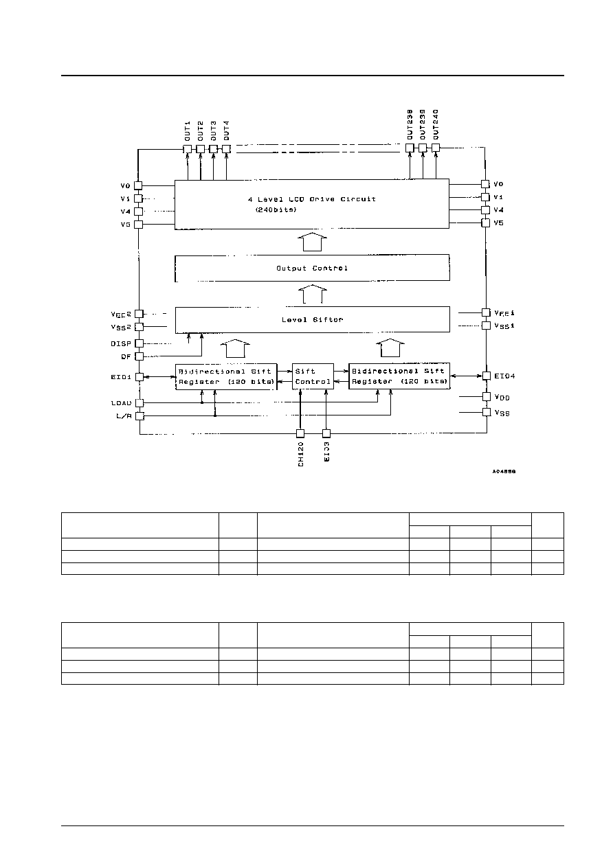
Block Diagram
No. 5279-3/8
LC4100C
Parameter
Symbol
Conditions
Ratings
Unit
min
typ
max
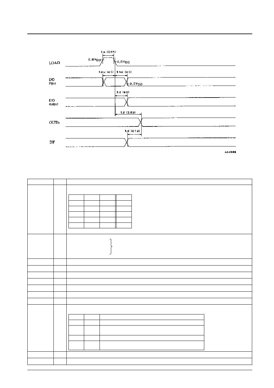
EIO output delay time
t
d (eo)
30 pF capacitance load: LOAD, EIO1, EIO4
180
ns
LOAD-OUTn delay time
t
d (ldo)
100 pF capacitance load: LOAD, OUTn
700
ns
DF-OUTn delay time
t
d (dfo)
100 pF capacitance load: DF, OUTn
1.2
µs
Switching Characteristics
at V
DD
= 5 V ± 10%, Ta = ≠20 to +75∞C
Parameter
Symbol
Conditions
Ratings
Unit
min
typ
max
EIO output delay time
t
d (eo)
30 pF capacitance load: LOAD, EIO1, EIO4
350
ns
LOAD-OUTn delay time
t
d (ldo)
100 pF capacitance load: LOAD, OUTn
3
µs
DF-OUTn delay time
t
d (dfo)
100 pF capacitance load: DF, OUTn
3
µs
Switching Characteristics
at V
DD
= 3 to 4.5 V, Ta = 25∞C ± 2∞C
No. 5279-4/8
LC4100C
Pin Functions
Symbol
I/O
Function
OUT1 to
OUT240
V
0
V
1
V
4
V
5
V
EE1
/V
EE2
V
SS1
/V
SS2
DISP
DF
LOAD
L/R
CH120
EIO1
EIO3
EIO4
V
DD
V
SS
O
I
I
I
I
≠
≠
I
I
I
I
I
I/O
I
I/O
--
--
Logic system power supply
Logic system ground
LCD drive outputs
Note:
*
don't care (0 or 1). These values must be fixed at either 0 or 1.
V
0
level drive voltage input
V
1
level drive voltage input
All pins with the same name must be set to the same potential.
V
4
level drive voltage input
V
5
level drive voltage input
High-voltage block power supply. V
EE1
and V
EE2
must have the same potential.
High-voltage block ground. V
SS1
and V
SS2
must have the same potential.
All outputs will be held at a fixed V
5
level when this pin is low.
Alternation input
Data shift pulse input (falling edge)
Data shift direction specification input
High: 120
◊
2, low: 240
◊
1
Enable inputs and outputs
DF
Data
DISP
OUTn
0
1
1
V
0
1
0
1
V
1
0
0
1
V
4
1
1
1
V
5
*
*
0
V
5
L/R
CH120
Shift direction
H
L
EIO1
OUT1
OUT240
EIO4
H
H
EIO1
OUT1
OUT120
EIO3
OUT121
OUT240
EIO4
L
L
EIO1
OUT1
OUT240
EIO4
L
H
EIO1
OUT1
OUT120
EIO3
OUT121
OUT240
EIO4
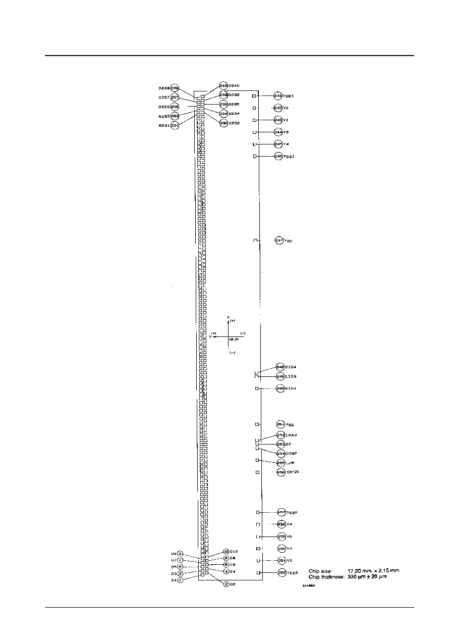
Pad Assignment
No. 5279-5/8
LC4100C
No. 5279-6/8
LC4100C
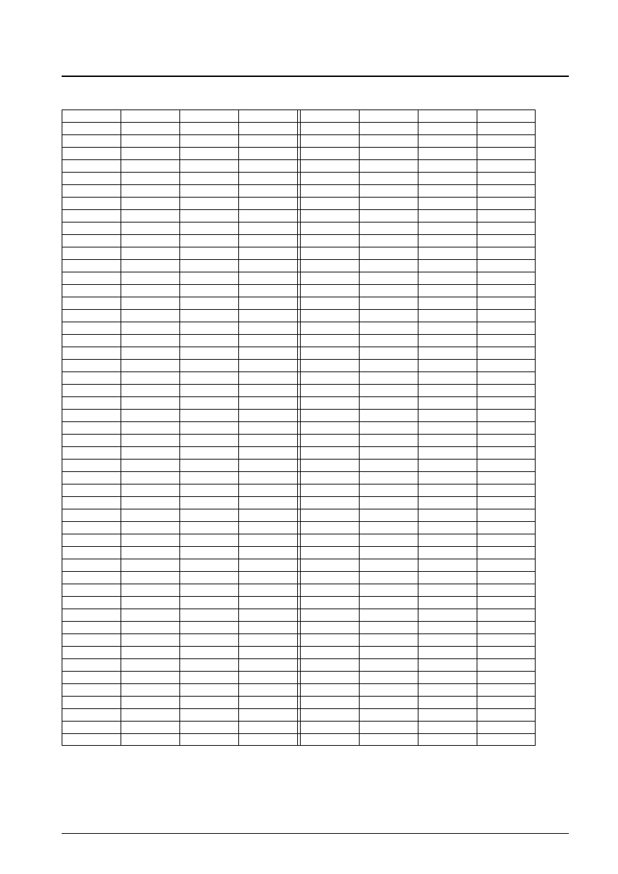
Pad Coordinates
Pad No.
Signal
X coordinate
Y coordinate
Pad No.
Signal
X coordinate
Y coordinate
1
OUT1
≠8365
897
51
OUT51
≠4865
897
2
OUT2
≠8295
727
52
OUT52
≠4795
727
3
OUT3
≠8225
897
53
OUT53
≠4725
897
4
OUT4
≠8155
727
54
OUT54
≠4655
727
5
OUT5
≠8085
897
55
OUT55
≠4585
897
6
OUT6
≠8015
727
56
OUT56
≠4515
727
7
OUT7
≠7945
897
57
OUT57
≠4445
897
8
OUT8
≠7875
727
58
OUT58
≠4375
727
9
OUT9
≠7805
897
59
OUT59
≠4305
897
10
OUT10
≠7735
727
60
OUT60
≠4235
727
11
OUT11
≠7665
897
61
OUT61
≠4165
897
12
OUT12
≠7595
727
62
OUT62
≠4095
727
13
OUT13
≠7525
897
63
OUT63
≠4025
897
14
OUT14
≠7455
727
64
OUT64
≠3955
727
15
OUT15
≠7385
897
65
OUT65
≠3885
897
16
OUT16
≠7315
727
66
OUT66
≠3815
727
17
OUT17
≠7245
897
67
OUT67
≠3745
897
18
OUT18
≠7175
727
68
OUT68
≠3675
727
19
OUT19
≠7105
897
69
OUT69
≠3605
897
20
OUT20
≠7035
727
70
OUT70
≠3535
727
21
OUT21
≠6965
897
71
OUT71
≠3465
897
22
OUT22
≠6895
727
72
OUT72
≠3395
727
23
OUT23
≠6825
897
73
OUT73
≠3325
897
24
OUT24
≠6755
727
74
OUT74
≠3255
727
25
OUT25
≠6685
897
75
OUT75
≠3185
897
26
OUT26
≠6615
727
76
OUT76
≠3115
727
27
OUT27
≠6545
897
77
OUT77
≠3045
897
28
OUT28
≠6475
727
78
OUT78
≠2975
727
29
OUT29
≠6405
897
79
OUT79
≠2905
897
30
OUT30
≠6335
727
80
OUT80
≠2835
727
31
OUT31
≠6265
897
81
OUT81
≠2765
897
32
OUT32
≠6195
727
82
OUT82
≠2695
727
33
OUT33
≠6125
897
83
OUT83
≠2625
897
34
OUT34
≠6055
727
84
OUT84
≠2555
727
35
OUT35
≠5985
897
85
OUT85
≠2485
897
36
OUT36
≠5915
727
86
OUT86
≠2415
727
37
OUT37
≠5845
897
87
OUT87
≠2345
897
38
OUT38
≠5775
727
88
OUT88
≠2275
727
39
OUT39
≠5705
897
89
OUT89
≠2205
897
40
OUT40
≠5635
727
90
OUT90
≠2135
727
41
OUT41
≠5565
897
91
OUT91
≠2065
897
42
OUT42
≠5495
727
92
OUT92
≠1995
727
43
OUT43
≠5425
897
93
OUT93
≠1925
897
44
OUT44
≠5355
727
94
OUT94
≠1855
727
45
OUT45
≠5285
897
95
OUT95
≠1785
897
46
OUT46
≠5215
727
96
OUT96
≠1715
727
47
OUT47
≠5145
897
97
OUT97
≠1645
897
48
OUT48
≠5075
727
98
OUT98
≠1575
727
49
OUT49
≠5005
897
99
OUT99
≠1505
897
50
OUT50
≠4935
727
100
OUT100
≠1435
727
Continued on next page.
No. 5279-7/8
LC4100C
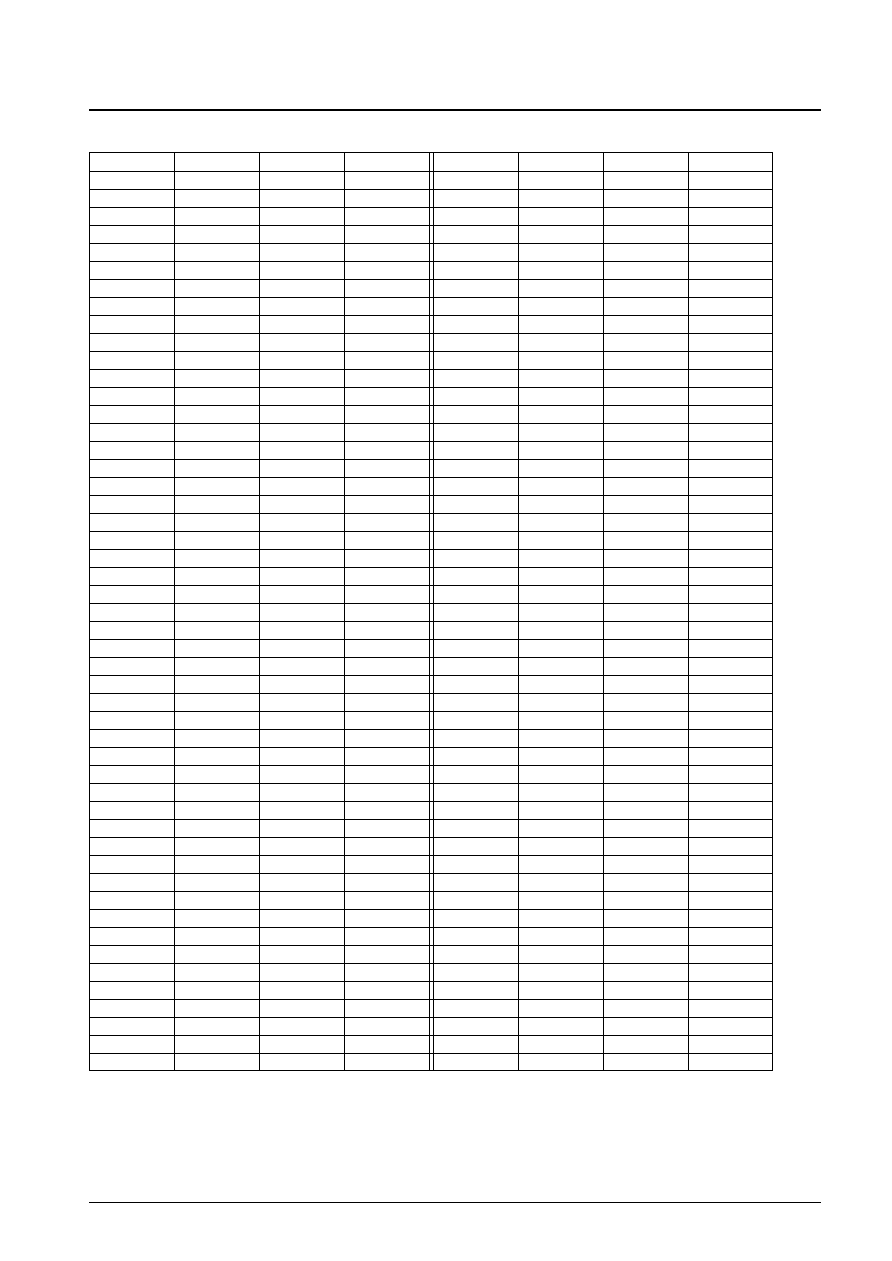
Continued from preceding page.
Pad No.
Signal
X coordinate
Y coordinate
Pad No.
Signal
X coordinate
Y coordinate
101
OUT101
≠1365
897
151
OUT151
2135
897
102
OUT102
≠1295
727
152
OUT152
2205
727
103
OUT103
≠1225
897
153
OUT153
2275
897
104
OUT104
≠1155
727
154
OUT154
2345
727
105
OUT105
≠1085
897
155
OUT155
2415
897
106
OUT106
≠1015
727
156
OUT156
2485
727
107
OUT107
≠945
897
157
OUT157
2555
897
108
OUT108
≠875
727
158
OUT158
2625
727
109
OUT109
≠805
897
159
OUT159
2695
897
110
OUT110
≠735
727
160
OUT160
2765
727
111
OUT111
≠665
897
161
OUT161
2835
897
112
OUT112
≠595
727
162
OUT162
2905
727
113
OUT113
≠525
897
163
OUT163
2975
897
114
OUT114
≠455
727
164
OUT164
3045
727
115
OUT115
≠385
897
165
OUT165
3115
897
116
OUT116
≠315
727
166
OUT166
3185
727
117
OUT117
≠245
897
167
OUT167
3255
897
118
OUT118
≠175
727
168
OUT168
3325
727
119
OUT119
≠105
897
169
OUT169
3395
897
120
OUT120
≠35
727
170
OUT170
3465
727
121
OUT121
35
897
171
OUT171
3535
897
122
OUT122
105
727
172
OUT172
3605
727
123
OUT123
175
897
173
OUT173
3675
897
124
OUT124
245
727
174
OUT174
3745
727
125
OUT125
315
897
175
OUT175
3815
897
126
OUT126
385
727
176
OUT176
3885
727
127
OUT127
455
897
177
OUT177
3955
897
128
OUT128
525
727
178
OUT178
4025
727
129
OUT129
595
897
179
OUT179
4095
897
130
OUT130
665
727
180
OUT180
4165
727
131
OUT131
735
897
181
OUT181
4235
897
132
OUT132
805
727
182
OUT182
4305
727
133
OUT133
875
897
183
OUT183
4375
897
134
OUT134
945
727
184
OUT184
4445
727
135
OUT135
1015
897
185
OUT185
4515
897
136
OUT136
1085
727
186
OUT186
4585
727
137
OUT137
1155
897
187
OUT187
4655
897
138
OUT138
1225
727
188
OUT188
4725
727
139
OUT139
1295
897
189
OUT189
4795
897
140
OUT140
1365
727
190
OUT190
4865
727
141
OUT141
1435
897
191
OUT191
4935
897
142
OUT142
1505
727
192
OUT192
5005
727
143
OUT143
1575
897
193
OUT193
5075
897
144
OUT144
1645
727
194
OUT194
5145
727
145
OUT145
1715
897
195
OUT195
5215
897
146
OUT146
1785
727
196
OUT196
5285
727
147
OUT147
1855
897
197
OUT197
5355
897
148
OUT148
1925
727
198
OUT198
5425
727
149
OUT149
1995
897
199
OUT199
5495
897
150
OUT150
2065
727
200
OUT200
5565
727
Continued on next page.
No. 5279-8/8
LC4100C
This catalog provides information as of September, 1996. Specifications and information herein are subject to
change without notice.
s
No products described or contained herein are intended for use in surgical implants, life-support systems, aerospace
equipment, nuclear power control systems, vehicles, disaster/crime-prevention equipment and the like, the failure of
which may directly or indirectly cause injury, death or property loss.
s
Anyone purchasing any products described or contained herein for an above-mentioned use shall:
Accept full responsibility and indemnify and defend SANYO ELECTRIC CO., LTD., its affiliates, subsidiaries and
distributors and all their officers and employees, jointly and severally, against any and all claims and litigation and all
damages, cost and expenses associated with such use:
Not impose any responsibility for any fault or negligence which may be cited in any such claim or litigation on
SANYO ELECTRIC CO., LTD., its affiliates, subsidiaries and distributors or any of their officers and employees
jointly or severally.
s
Information (including circuit diagrams and circuit parameters) herein is for example only; it is not guaranteed for
volume production. SANYO believes information herein is accurate and reliable, but no guarantees are made or implied
regarding its use or any infringements of intellectual property rights or other rights of third parties.
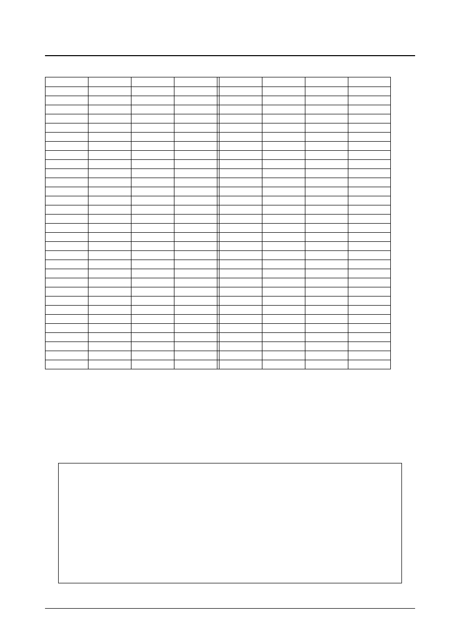
Continued from preceding page.
Pad No.
Signal
X coordinate
Y coordinate
Pad No.
Signal
X coordinate
Y coordinate
201
OUT201
5635
897
232
OUT232
7805
727
202
OUT202
5705
727
233
OUT233
7875
897
203
OUT203
5775
897
234
OUT234
7945
727
204
OUT204
5845
727
235
OUT235
8015
897
205
OUT205
5915
897
236
OUT236
8085
727
206
OUT206
5985
727
237
OUT237
8155
897
207
OUT207
6055
897
238
OUT238
8225
727
208
OUT208
6125
727
239
OUT239
8295
897
209
OUT209
6195
897
240
OUT240
8365
727
210
OUT210
6265
727
241
V
EE1
8295
≠886
211
OUT211
6335
897
242
V
0
7895
≠863
212
OUT212
6405
727
243
V
1
7495
≠859
213
OUT213
6475
897
244
V
5
7095
≠859
214
OUT214
6545
727
245
V
4
6695
≠859
215
OUT215
6615
897
246
V
SS1
6295
≠859
216
OUT216
6685
727
247
V
DD
3295
≠870
217
OUT217
6755
897
248
EIO4
≠1295
≠870
218
OUT218
6825
727
249
EIO3
≠1495
≠870
219
OUT219
6895
897
250
EIO1
≠1895
≠870
220
OUT220
6965
727
251
V
SS
≠3095
≠887
221
OUT221
7035
897
252
LOAD
≠3695
≠870
222
OUT222
7105
727
253
DF
≠3895
≠870
223
OUT223
7175
897
254
DISP
≠4095
≠870
224
OUT224
7245
727
255
L/R
≠4495
≠870
225
OUT225
7315
897
256
CH120
≠4895
≠870
226
OUT226
7385
727
257
V
SS2
≠6295
≠859
227
OUT227
7455
897
258
V
4
≠6695
≠859
228
OUT228
7525
727
259
V
5
≠7095
≠859
229
OUT229
7595
897
260
V
1
≠7495
≠859
230
OUT230
7665
727
261
V
0
≠7895
≠863
231
OUT231
7735
897
262
V
EE2
≠8295
≠886