 | –≠–ª–µ–∫—Ç—Ä–æ–Ω–Ω—ã–π –∫–æ–º–ø–æ–Ω–µ–Ω—Ç: LC4101C | –°–∫–∞—á–∞—Ç—å:  PDF PDF  ZIP ZIP |

Overview
The LC4101C is a segment driver for large-scale dot
matrix LCD panels. It latches 240 bits of display data sent
from the controller over a 4-bit or 8-bit parallel connection
and generates the LCD drive signals. The LC4100C and
LC4101C form a large-screen LCD panel driver chip set.
Features
∑ Fabricated in a CMOS (P-sub) high-voltage process.
∑ LCD drive voltage: 36 V
∑ Logic system power-supply voltage: 3.0 to 5.5 V
∑ f
cp
max: 12 MHz (V
DD
= 5 V ±10 %), 6.5 MHz (V
DD
= 3 to 4.5 V)
∑ 240 outputs
∑ Parallel input switchable between 4 and 8 bits
∑ DISPOFF function that locks the drive voltages output
to the LCD at fixed levels.
∑ Display duty: 1/160 to 1/480
CMOS LSI
Ordering number : EN5280A
O3096HA (OT)/43096HA (OT) No. 5280-1/9
SANYO Electric Co.,Ltd. Semiconductor Bussiness Headquarters
TOKYO OFFICE Tokyo Bldg., 1-10, 1 Chome, Ueno, Taito-ku, TOKYO, 110 JAPAN
LCD Dot Matrix Segment Driver
for STN Displays
LC4101C
Specifications
Absolute Maximum Ratings
at Ta = 25∞C ± 2∞C, standard V
SS
, V
EEn
= V
EE1
or V
EE2
, V
SSn
= V
SS1
or V
SS2
Note: The voltages V
0
, V
2
, V
3
, and V
5
must obey the relationships V
EEn
V
0
V
2
V
EE
≠ 7, and 7
V
3
V
5
V
SSn
. (Unit: V)
Parameter
Symbol
Conditions
Ratings
Unit
V
DD
≠0.3 to +7
V
Supply voltage
V
EEn
≠0.3 to +40
V
V
SSn
≠0.3 to +0.3
V
V
IN
D0 to D7, LOAD, CP, L/R, BS, TEST,
≠0.3 to V
DD
+ 0.3
V
DISP, DF, EIO1, EIO2
Input voltage
V
0
, V
2
V
0
, V
2
V
EEn
≠ 7 to V
EEn
+ 0.3
V
V
3
V
3
≠0.3 to V
SSn
+ 7
V
V
5
V
5
≠0.3 to +0.3
V
Operating temperature
Topr
≠20 to +75
∞C
Storage temperature
Tstg
≠55 to +125
∞C
Allowable Operating Ranges
at Ta = ≠20 to +75∞C, standard V
SS
, V
EEn
= V
EE1
or V
EE2
, V
SSn
= V
SS1
or V
SS2
Note: 1. The voltages V
0
, V
2
, V
3
, and V
5
must obey the relationships V
EEn
V
0
V
2
V
EE
≠ 7, and 7
V
3
V
5
V
SSn
. (Unit: V)
2. When turning on the power supplies, first turn on the logic system power supply and then turn on the high-voltage system power supply;
alternatively, turn both on at the same time.
When turning off the power supplies, first turn off the high-voltage system power supply and then turn off the logic system power supply;
alternatively, turn both off at the same time.
No. 5280-2/9
LC4101C
Parameter
Symbol
Conditions
min
typ
max
Unit
V
DD
3.0
5.5
V
Supply voltage
V
EEn
20
36
V
V
SSn
0
V
Input high-level voltage
V
IH
D0 to D7, CP, L/R, BS, DF, TEST, DISP,
0.8 V
DD
V
DD
V
EIO1, EIO2, LOAD
Input low-level voltage
V
IL
D0 to D7, CP, L/R, BS, DF, TEST, DISP,
0
0.2 V
DD
V
EIO1, EIO2, LOAD
V
0
, V
2
V
0
, V
2
V
EEn
≠ 7
V
EEn
V
Input voltage
V
3
V
3
0
V
SSn
+ 7
V
V
5
V
5
0
V
CP clock frequency
f
cp
CP
12
MHz
High-level load
t
w (ldh)
LOAD
50
ns
pulse width
High-level clock
t
w (cph)
CP
28
ns
pulse width
Low-level clock
t
w (cpl)
CP
28
ns
V
DD
=
pulse width
5 V ± 10%
Load clock frequency
f
load
LOAD
1
MHz
LOAD/CP setup time
t
su (ld)
LOAD, CP
30
ns
LOAD/CP hold time
t
ho (ld)
LOAD, CP
200
ns
DATA/CP setup time
t
su (cp)
CP, D0 to D7
28
ns
DATA/CP hold time
t
ho (cp)
CP, D0 to D7
20
ns
EIO input setup time
t
su (ei)
CP, EIO1, EIO2
30
ns
Clock rise time
t
r
LOAD, CP
50
ns
Clock fall time
t
f
LOAD, CP
50
ns
CP clock frequency
f
cp
CP
6.5
MHz
High-level load
t
w (ldh)
LOAD
50
ns
pulse width
High-level clock
t
w (cph)
CP
40
ns
pulse width
Low-level clock
t
w (cpl)
CP
40
ns
V
DD
=
pulse width
3 to 4.5 V
Load clock frequency
f
load
LOAD
200
kHz
LOAD/CP setup time
t
su (ld)
LOAD, CP
35
ns
LOAD/CP hold time
t
ho (ld)
LOAD, CP
350
ns
DATA/CP setup time
t
su (cp)
CP, D0 to D7
50
ns
DATA/CP hold time
t
ho (cp)
CP, D0 to D7
50
ns
EIO input setup time
t
su (ei)
CP, EIO1, EIO2
45
ns
Clock rise time
t
r
LOAD, CP
50
ns
Clock fall time
t
f
LOAD, CP
50
ns

Electrical Characteristics
at Ta = ≠20 to +75∞C, standard V
SS
, V
DD
= 3 to 5.5 V
Note: 1. With LOAD = 28 kHz, fcp = 6.5 MHz, f
DF
= 75 Hz, or with no output load. Input voltages V
IH
and V
IL
must be V
DD
and V
SS,
respectively.
2. The standby current drain rating assumes that the EIOn (input) are at V
DD
.
Block Diagram
No. 5280-3/9
LC4101C
Parameter
Symbol
Conditions
min
typ
max
Unit
Input high-level current
I
IH
V
IN
= V
DD
: D0 to D7, CP, L/R, BS, DF, TEST, DISP,
1
EIO1, EIO2, LOAD
µA
Input low-level current
I
IL
V
IN
= V
SS
: D0 to D7, CP, L/R, BS, DF, TEST, DISP,
≠1
µA
EIO1, EIO2, LOAD
Output high-level voltage
V
OH
I
O
= ≠0.4 mA: EIO1, EIO2
0.8 V
DD
V
DD
V
Output low-level voltage
V
OL
I
O
= 0.4 mA: EIO1, EIO2
V
SS
0.2 V
DD
V
V
EE
= 20 V, V
0
≠ V
0
= 0.5 V, V
2
≠ V
0
= 0.5 V,
Output on resistance
R
OUT
V
0
≠ V
3
= 0.5 V, V
0
≠ V
5
= 0.5 V, V
0
= 20 V,
0.8
1.6
k
V
2
= 20 V, V
3
= 0 V, V
5
= 0 V: OUT1 to OUT240
Current drain
I
DD
V
DD
= 3 to 5.5 V
7.5
µA
Operating current drain
I
EE
V
DD
= 3 to 5.5 V, V
EEn
= 26 V
*
1
3.0
mA
V
DD
= 5 V ± 10%, V
EEn
= 36 V
3.0
mA
Static current
Istb
*
2
750
µA

Switching Characteristics
at V
DD
= 5 V ± 10%, Ta = ≠20 to +75∞C
at V
DD
= 3 to 4.5 V, Ta = ≠20 to +75∞C
Note: 1. Since this IC detects the EIO inputs on the rising edge of the CP signal, the EIO inputs must be set up before the first data is input. As a result, a
tho(ld) clock stop period is required directly after the rise of the LOAD signal if the clock frequency is relatively high.
Note: 2. If this IC is used with a 4-bit width data input, the number of data clocks between one LOAD and the next LOAD must be doubled.
No. 5280-4/9
LC4101C
Parameter
Symbol
Conditions
min
typ
max
Unit
EIO output delay time
t
d (eo)
30 pF capacitive load
39
ns
LD/EIO output delay time
t
d (leo)
30 pF capacitive load
70
ns
LOAD-OUTn delay time
t
d (ldo)
100 pF capacitive load
700
µs
DF-OUTn delay time
t
d (dfo)
100 pF capacitive load
1.4
µs
Parameter
Symbol
Conditions
min
typ
max
Unit
EIO output delay time
t
d (eo)
30 pF capacitive load
80
ns
LD/EIO output delay time
t
d (leo)
30 pF capacitive load
130
ns
LOAD-OUTn delay time
t
d (ldo)
100 pF capacitive load
3
µs
DF-OUTn delay time
t
d (dfo)
100 pF capacitive load
3
µs

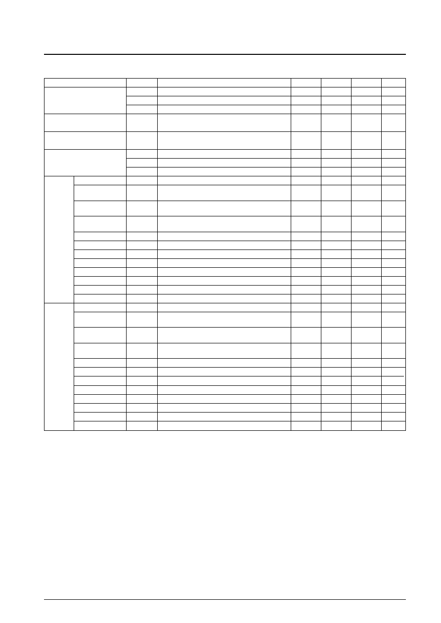
Pin Functions
No. 5280-5/9
LC4101C
Symbol
I/O
Function
OUT1 to
OUT240
V
0
V
2
V
3
V
5
V
EE1
/V
EE2
V
SS1
/V
SS2
DISP
DF
LOAD
L/R
EIO1
EIO2
O
I
I
I
I
≠
≠
I
I
I
I
I/O
I/O
LCD drive outputs
Note:
*
don't care (0 or 1).
V
0
level drive voltage input
V
2
level drive voltage input
All pins with the same name must be set to the same potential.
V
3
level drive voltage input
V
5
level drive voltage input
High-voltage block power supply. V
EE1
and V
EE2
must have the same potential.
High-voltage block ground. V
SS1
and V
SS2
must have the same potential.
All outputs will be held at a fixed V
5
level when this pin is low.
Alternation input
CP
I
Data acquisition clock (falling edge)
Data load clock (falling edge)
BS
I
4-bit/8-bit switching signal; high: 8 bits, low: 4 bits
8
◊
30: Data latch (BS = high)
Note: The numbers 1 to 240 in the table indicate OUT output numbers.
Enable inputs and outputs
Enable inputs: Tie the first stage enable input to V
SS
, and then connect the enable input of each following stage to the enable
output of the preceding stage.
Enable outputs: When connecting multiple chips in cascade, connect the enable output to the enable input of the next stage.
DF
Data
DISP
OUTn
1
1
1
V
0
1
0
1
V
2
0
0
1
V
3
0
1
1
V
5
*
*
0
V
5
L/R
EIO1
EIO2
L
In
Out
H
Out
In
L/R
CP:
1
2
3
4
29
30
D7
1
9
17
25
∑ ∑ ∑
225
233
D6
2
10
18
26
∑ ∑ ∑
226
234
D5
3
11
19
27
∑ ∑ ∑
227
235
L
D4
4
12
20
28
∑ ∑ ∑
228
236
D3
5
13
21
29
∑ ∑ ∑
229
237
D2
6
14
22
30
∑ ∑ ∑
230
238
D1
7
15
23
31
∑ ∑ ∑
231
239
D0
8
16
24
32
∑ ∑ ∑
232
240
D7
240
232
224
216
∑ ∑ ∑
16
8
D6
239
231
223
215
∑ ∑ ∑
15
7
D5
238
230
222
214
∑ ∑ ∑
14
6
H
D4
237
229
221
213
∑ ∑ ∑
13
5
D3
236
228
220
212
∑ ∑ ∑
12
4
D2
235
227
219
211
∑ ∑ ∑
11
3
D1
234
226
218
210
∑ ∑ ∑
10
2
D0
233
225
217
209
∑ ∑ ∑
9
1
Continued on next page.