Overview
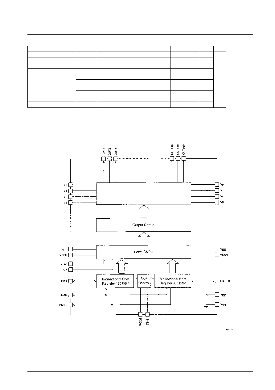
The LC4102C is a common driver for large-scale dot
matrix LCD panels. It includes a 160-bit bidirectional shift
register and 4-level LCD driver circuits. The number of
bits can be further increased by using the provided input
and output pins to connect multiple LC4102Cs in cascade.
The LC4102C and LC4104C form a large-screen LCD
panel driver chip set.
Features
∑ Fabricated in a CMOS (P-sub) high-voltage process.
∑ LCD drive voltage: 36 V
∑ Logic system power-supply voltage: 2.7 to 5.5 V
∑ fcp max: 2.5 MHz
∑ Slim chip (output pads are concentrated on one of the
longer sides)
∑ Bidirectional shift register
∑ The shift register can be split into two 80-bit registers.
(Two screens drivable)
∑ DISPOFF function that locks the drive voltages output
to the LCD at fixed levels.
∑ Display duty: 1/160 to 1/480
∑ Appropriate for COG (chip on glass) mounting. (A gold
bump structure is adopted in the pad areas.)
CMOS LSI
Ordering number : EN5789A
43098HA (OT)/82097HA (OT) No. 5789-1/8
SANYO Electric Co.,Ltd. Semiconductor Bussiness Headquarters
TOKYO OFFICE Tokyo Bldg., 1-10, 1 Chome, Ueno, Taito-ku, TOKYO, 110-8534 JAPAN
LCD Dot Matrix Common Driver
for STN Displays
LC4102C
Specifications
The electrical characteristics values shown below are for devices packaged in the Sanyo standard PGA-208 package.
Absolute Maximum Ratings
at V
SS
= 0
Note: 1. LOAD, RS/LS, DISP, DF, DIO1, DIO160, DMIN and MODE
2. The voltages V0, V1, V4, and V5 must obey the relationships V
EE
V0
V1
V
EE
≠ 7 V, and 7 V
V4
V5
V
SSH
.
Allowable Operating Ranges
at V
SS
= 0, Ta = ≠20 to +75
∞
C
Note: 1. LOAD, RS/LS, DISP, DF, DIO1, DIO160, DMIN and MODE
2. The voltages V0, V1, V4, and V5 must obey the relationships V
EE
V0
V1
V
EE
≠ 7 V, and 7 V
V4
V5
V
SSH
.
When turning on the power supplies, first turn on the logic system power supply and then turn on the high-voltage system power supply; alternatively,
turn both on at the same time.
When turning off the power supplies, first turn off the high-voltage system power supply and then turn off the logic system power supply; alternatively,
turn both off at the same time.
Parameter
Symbol
Applicable pins
min
typ
max
Unit
V
DD
max
V
DD
≠0.3
7.0
V
Supply voltage
V
EE
max
V
EE
≠0.3
40.0
V
V
SS
max
V
SSH
≠0.3
0.3
V
V
IN
*
1
≠0.3
V
DD
+ 0.3
V
Input voltage
V0, V1
V0, V1
*
2
V
EE
≠ 7.0
V
EE
+ 0.3
V
V4
V4
*
2
≠0.3
V
SS
+ 7.0
V
V5
V5
*
2
≠0.3
+0.3
V
Operating temperature
Topr
≠20
+75
∞C
Storage temperature
Tstg
≠55
+125
∞C
Parameter
Symbol
Applicable pins
min
typ
max
Unit
V
DD
V
DD
2.7
5.5
V
Supply voltage
V
EE
V
EE
14
36
V
V
SSH
V
SSH
0
V
Input high-level voltage
V
IH
*
1
0.8
◊
V
DD
V
DD
V
Input low-level voltage
V
IL
*
1
0
0.2
◊
V
DD
V
V0, V1
V0, V1
*
2
V
EE
≠ 7.0
V
EE
V
Input voltage
V4
V4
*
2
0
V
SSH
+ 7.0
V
V5
V5
*
2
0
V
Electrical Characteristics
at Ta = ≠20 to +75∞C, V
DD
= 2.7 to 5.5 V, V
SS
= 0 V
Note: 1. LOAD, RS/LS, DISP, DF, DIO1, DIO160, DMIN and MODE
2. V
OUT
is the voltage applied by on-state outputs. V0 = V
EE
, V1 = 19/20 (V
EE
≠ V
SSH
), V4 = 1/20 (V
EE
≠ V
SSH
), V5 = V
SSH
, V
SSH
= V
SS
3. V
DD
= 2.7 to 5.5 V, f
CP
= 50 kHz
4. f
DF
= 100 Hz, with no output load, V
EE
= 36 V, for a single data shift
Block Diagram
No. 5789-2/8
LC4102C
Parameter
Symbol
Conditions
min
typ
max
Unit
Input high-level current
I
IH
V
IN
= V
DD
*
1
1
µA
Input low-level current
I
IL
V
IN
= V
SS
*
1
≠1
Output high-level voltage
V
OH
I
OH
= ≠0.4 mA, DIO1, DIO160
0.8
◊
V
DD
V
DD
V
Output low-level voltage
V
OL
I
OL
= 0.4 mA, DIO1, DIO160
V
SS
0.2
◊
V
DD
RON0
V
OUT
= V0 ≠ 0.5 V
*
2
, OUT1 to 160
1000
Output on resistance
RON1
V
OUT
= V1 ≠ 0.5 V
*
2
, OUT1 to 160
1000
RON4
V
OUT
= V4 + 0.5 V
*
2
, OUT1 to 160
1000
RON5
V
OUT
= V5 + 0.5 V
*
2
, OUT1 to 160
1000
Current drain 1
I
DD
V
DD
*
3
200
µA
Current drain 2
I
DDH
V
DD
*
4
500
4-Level LCD Driver CIRCUIT (160 bits)
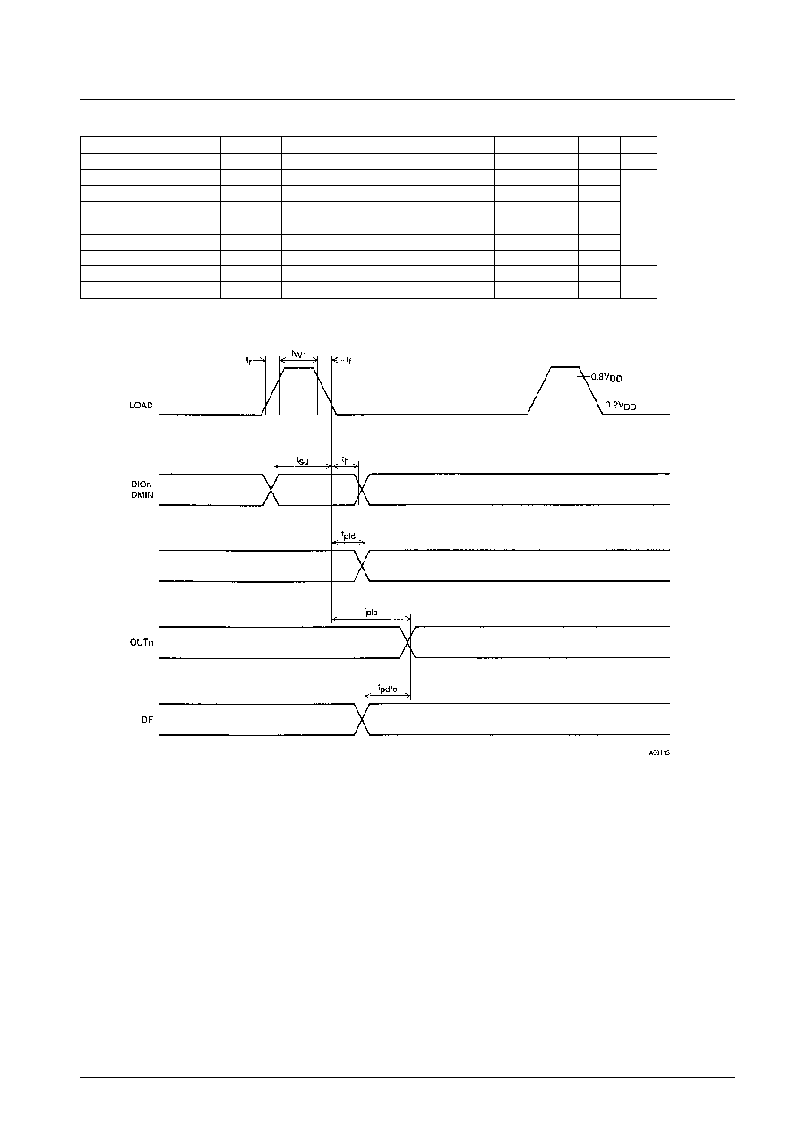
Switching Characteristics
at V
DD
= 2.7 to 5.5 V, Ta = ≠20 to +75∞C, V
SS
= 0 V
Switching Characteristics
No. 5789-3/8
LC4102C
Parameter
Symbol
Conditions
min
typ
max
Unit
Clock frequency
fload
LOAD
2.5
MHz
High-level clock pulse width
twl
LOAD
100
Input setup time
tsu
LOAD, DIOn
100
Input hold time
th
DMIN
30
LOAD falling time
tr
LOAD
30
ns
LOAD rising time
tf
LOAD
30
DIO output delay time
tpld
LOAD, DIOn: 30 pF capacitance load
200
LOAD-on delay time
tplo
LOAD, OUTn: 100 pF capacitance load
1.0
µs
DF-on delay time
tpdfo
DF, OUTn: 100 pF capacitance load
1.0
DIO output
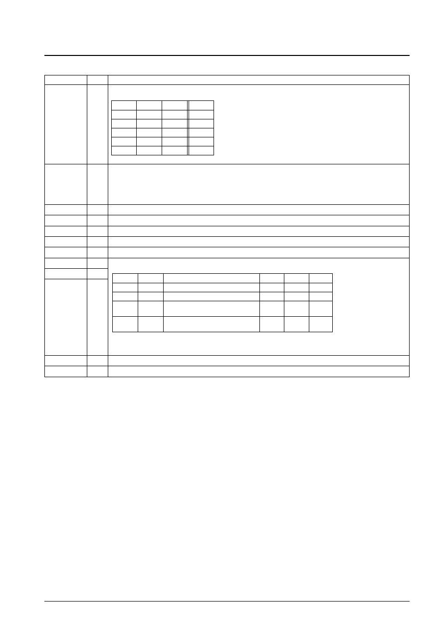
Pin Functions
No. 5789-4/8
LC4102C
Symbol
I/O
Function
OUT1 to
OUT160
V0
V1
V4
V5
V
EE
V
SSH
DISP
DF
LOAD
MODE
RS/LS
DIO1
DMIN
DIO160
V
DD
V
SS
O
I
I
I
I
≠
≠
I
I
I
I
I
I/O
I
I/O
--
--
Logic system power supply
Logic system ground
LCD drive outputs
V0 level drive voltage input
V1 level drive voltage input
V4 level drive voltage input
V5 level drive voltage input
High-voltage block power supply
High-voltage block ground
All outputs will be held at a fixed V5 level when this pin is low.
Alternation input
Data shift pulse input (falling edge)
Data shift direction specification input
*
: don't care
DF
Data
DISP
OUTn
L
H
H
V0
H
L
H
V1
L
L
H
V4
H
H
H
V5
*
*
L
V5
MODE
RS/LS
Shift direction
DIO1
DIO160
DMIN
L
L
OUT160
OUT1
OUT
IN
*
L
H
OUT1
OUT160
IN
OUT
*
H
L
OUT160
OUT81
OUT
IN
IN
OUT80
OUT1
H
H
OUT1
OUT80
IN
OUT
IN
OUT81
OUT160
*
: don't care (Must be fixed at low or high.)
Note:
*
This IC is sensitive to ESD care must be used when handling this device.