 | –≠–ª–µ–∫—Ç—Ä–æ–Ω–Ω—ã–π –∫–æ–º–ø–æ–Ω–µ–Ω—Ç: LC4104C | –°–∫–∞—á–∞—Ç—å:  PDF PDF  ZIP ZIP |

Overview
The LC4104 is a segment driver LSI for large-scale dot
matrix LCD displays. The LC4104 latches 160-bits of
display data transferred from the controller over a 4- or 8-
bit parallel interface and generates the LCD drive signals.
In conjunction with the LC4102 common driver, the
LC4104 forms a chip set that can drive large-screen LCD
panels.
Features
∑ High-voltage CMOS (P-sub) process
∑ LCD drive voltage: 36 V
∑ Logic system power-supply voltage: 2.7 to 5.5 V
∑ Maximum fcp: 12 MHz (V
DD
= 5 V ±10%),
10 MHz (V
DD
= 2.7 to 4.5 V)
∑ Slim chip (The output pads are located along one of the
long sides.)
∑ Parallel input circuit can be switched between 4 and
8 bits.
∑ Output directionality switching
∑ DISPOFF function (Holds the LCD drive voltage at a
fixed level.)
∑ Display duty ratios: 1/160 to 1/480
∑ Appropriate for COG (chip on glass) mounting. (A gold
bump structure is adopted in the pad areas.)
∑ LC4104C: Chip product
CMOS LSI (P-sub)
Ordering number : EN
*
5194D
43098HA (OT)/73097HA (OT)/D3095HA (OT) No. 5194-1/9
Preliminary
SANYO Electric Co.,Ltd. Semiconductor Bussiness Headquarters
TOKYO OFFICE Tokyo Bldg., 1-10, 1 Chome, Ueno, Taito-ku, TOKYO, 110-8534 JAPAN
LCD Dot Matrix Segment Driver
for STN Displays
LC4104C
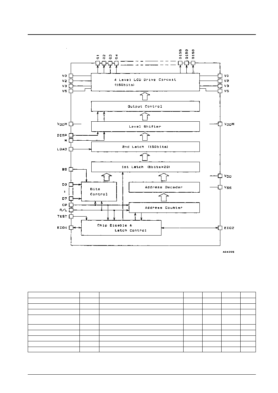
Block Diagram
Specifications
The following electrical characteristics apply when sealed in a Sanyo standard PGA-208 package.
Absolute Maximum Ratings
at V
SS
= 0 V
Note: V0, V2, V3, and V5 must obey the following inequalities: V
DDH
V0
V2
V
DDH
≠ 7 V, and 7 V
V3
V5
V
SS
.
No. 5194-2/9
LC4104C
Parameter
Symbol
Conditions
min
typ
max
Unit
Maximum supply voltage
V
DD
max
≠0.3
7
V
Maximum supply voltage
V
DDH
max
≠0.3
40
V
Maximum supply voltage
V
SS
max
≠0.3
+0.3
V
Input voltage
V
IN
D0 to D7, LOAD, CP, R/L, TEST, DISP, M, EIO1, EIO2,
≠0.3
V
DD
+ 0.3
V
BS
Input voltage
V0, V2
V0, V2
V
DDH
≠ 7
V
DDH
+ 0.3
V
Input voltage
V3
V3
≠0.3
V
SS
+ 7
V
Input voltage
V5
V5
≠0.3
+0.3
V
Operating temperature
Topr
≠20
+75
∞C
Storage temperature
Tstg
≠55
+125
∞C

Allowable Operating Ranges
at Ta = ≠20 to +75∞C, V
SS
= 0 V
Note: V0, V2, V3, and V5 must obey the following inequalities: V
DDH
V0
V2
V
DDH
≠ 7 V, and 7 V
V3
V5
V
SS
.
At power on: First turn on the logic system power supply and then turn on the high-voltage system power supply.
At power off: First turn off the high-voltage system power supply and then turn off the logic system power supply.
Allowable Operating Ranges
at Ta = ≠20 to +75∞C, V
SS
= 0 V, V
DD
= 5 V ± 10%
Note:
*
The clock rise time (tr) and fall time (tf) must obey inequalities
and
y
below.
: tr, tf <
y
: tr, tf
50 ns
Allowable Operating Ranges
at Ta = ≠20 to +75∞C, V
SS
= 0 V, V
DD
= 2.7 to 4.5 V
Note:
*
The clock rise time (tr) and fall time (tf) must obey inequalities
and
y
below.
: tr, tf <
y
: tr, tf
50 ns
1
≠ tw (cph) ≠ tw (cpl)
fcp
2
1
≠ tw (cph) ≠ tw (cpl)
fcp
2
No. 5194-3/9
LC4104C
Parameter
Symbol
Conditions
min
typ
max
Unit
Supply voltage
V
DD
2.7
5.5
V
Supply voltage
V
DDH
20
36
V
Supply voltage
V
SS
0
V
Input high-level voltage
V
IH
D0 to D7, LOAD, CP, R/L, M, TEST, DISP, BS,
0.8 V
DD
V
DD
V
EIO1, EIO2
Input low-level voltage
V
IL
D0 to D7, LOAD, CP, R/L, M, TEST, DISP, BS,
0
0.2 V
DD
V
EIO1, EIO2
Input voltage
V0, V2
V0, V2
V
DDH
≠ 7
V
DDH
V
Input voltage
V3
V3
0
V
SSH
+ 7
V
Input voltage
V5
V5
0
V
Parameter
Symbol
Conditions
min
typ
max
Unit
CP clock frequency
fcp
CP
12
MHz
High-level load pulse width
tw (ldH)
LOAD
50
ns
High-level clock pulse width
tw (cpH)
CP
20
ns
Low-level clock pulse width
tw (cpL)
CP
20
ns
LOAD/CP setup time
tsu (ld)
LOAD, CP
100
ns
LOAD/CP hold time
tho (ld)
LOAD, CP
200
ns
DATA/CP setup time
tsu (cp)
CP, D0 to D7
10
ns
DATA/CP hold time
tho (cp)
CP, D0 to D7
10
ns
EIO input setup time
tsu (ei)
CP, EIO1, EIO2
24
ns
Clock rise time
tr
LOAD, CP
*
50
ns
Clock fall time
tf
LOAD, CP
*
50
ns
Parameter
Symbol
Conditions
min
typ
max
Unit
CP clock frequency
fcp
CP
10
MHz
High-level load pulse width
tw (ldH)
LOAD
50
ns
High-level clock pulse width
tw (cpH)
CP
37
ns
Low-level clock pulse width
tw (cpL)
CP
37
ns
LOAD/CP setup time
tsu (ld)
LOAD, CP
100
ns
LOAD/CP hold time
tho (ld)
LOAD, CP
200
ns
DATA/CP setup time
tsu (cp)
CP, D0 to D7
35
ns
DATA/CP hold time
tho (cp)
CP, D0 to D7
35
ns
EIO input setup time
tsu (ei)
CP, EIO1, EIO2
30
ns
Clock rise time
tr
LOAD, CP
*
50
ns
Clock fall time
tf
LOAD, CP
*
50
ns

Electrical Characteristics
at Ta = ≠20 to +75∞C, V
DD
= 2.7 to 5.5 V, V
SS
= 0 V
Note: 1. V
O
is the voltage applied for an on output, V0 = V
DDH
, V2 = 18/20 (V
DDH
≠ V
SS
), V3 = 2/20 (V
DDH
≠ V
SS
), V5 = V
SS
2. LOAD = 28 kHz, CP = 10 MHz, M = 75 Hz
Alternatively: No output load and with the inputs V
IH
= V
DD
and V
IL
= V
SS
.
3. The current drain in standby mode. Note that the EIOn pins must be held at V
DD
.
Switching Characteristics
at Ta = ≠20 to +75∞C, V
SS
= 0 V, V
DD
= 5 V ± 10%
Switching Characteristics
at Ta = ≠20 to +75∞C, V
SS
= 0 V, V
DD
= 2.7 to 4.5 V
Timing Chart
No. 5194-4/9
LC4104C
Parameter
Symbol
Conditions
min
typ
max
Unit
Input high-level current
I
IH
V
IN
= V
DD
: D0 to D7, LOAD, CP, R/L, M, DISP,
5
µA
EIO1, EIO2, BS, TEST
I
IL
1
V
IN
= V
SS
: D0 to D7, LOAD, CP, R/L, M, TEST, DISP,
≠5
Input low-level current
EIO1, EIO2, BS
µA
I
IL
2
V
IN
= V
SS
: TEST
≠500
Output high-level voltage
V
OH
I
O
= ≠0.4 mA: EIO1, EIO2
V
DD
≠ 0.4
V
DD
V
Output low-level voltage
V
OL
I
O
= 0.4 mA: EIO1, EIO2
V
SS
0.4
V
Output on resistance
R
OUT
V
DDH
= 36 V
*
1
, V0 ≠ V
O
= 0.5 V, V2 ≠ V
O
= 0.5 V,
1
3
k
V
O
≠ V3 = 0.5 V, V
O
≠ V5 = 0.5 V: O1 to O160
I
DD
V
DD
= 2.7 to 5.5 V
5.0
mA
Current drain
I
DDH
V
DD
= 2.7 to 5.5 V, V
DDH
= 32 V
*
2
,
2.0
mA
V
DD
= 5 V ± 10%, V
DDH
= 36 V
2.0
mA
I
ST
*
3
500
µA
Parameter
Symbol
Conditions
min
typ
max
Unit
EIO output delay time
td (eo)
30 pF capacitive load: CP, EIO1, EIO2
40
ns
LD/EIO output delay time
td (leo)
30 pF capacitive load: LOAD, EIO1, EIO2
70
ns
LOAD/on delay time
td (ldo)
100 pF capacitive load: LOAD, O1 to O160
700
ns
M/on delay time
td (mo)
100 pF capacitive load: M, O1 to O160
700
ns
Parameter
Symbol
Conditions
min
typ
max
Unit
EIO output delay time
td (eo)
30 pF capacitive load: CP, EIO1, EIO2
80
ns
LD/EIO output delay time
td (leo)
30 pF capacitive load: LOAD, EIO1, EIO2
130
ns
LOAD/on delay time
td (ldo)
100 pF capacitive load: LOAD, O1 to O160
3
µs
M/on delay time
td (mo)
100 pF capacitive load: M, O1 to O160
3
µs

Pin Functions
No. 5194-5/9
LC4104C
Symbol
I/O
Function
O1 to O160
V0
V2
V3
V5
V
DDH
V
DD
V
SS
DISP
M
EIO1
EIO2
CP
LOAD
TEST
R/L
D0 to D7
BS
O
I
I
I
I
--
--
--
I
I
I/O
I/O
I
I
I
I
I
I
LCD drive outputs
V0 level drive voltage supply (selected level)
V2 level drive voltage supply (unselected level)
V3 level drive voltage supply (unselected level)
V5 level drive voltage supply (selected level)
High-voltage system power supply. Pins with the same name must be set to the same potential.
Logic system power supply.
GND
LCD off function. All outputs go to the V5 level when this pin is low.
Alternation signal input
Enable I/O
Enable input:
The enable input at the first stage is fixed at V
SS
. For succeeding stages, the enable input is connected to the
enable output from the preceding stage.
Enable output: Connected to the enable input of the next stage when cascode connection is used.
Data acquisition clock (falling edge)
Data load clock (falling edge)
Test input. Must be tied high in normal use.
*
Data shift direction setting
Parallel data inputs
Input bus setting. Set high for 8-bit input, low for 4-bit input. For 4-bit input, D0 to D3 are used for data input and D4 to D7 must
be tied to ground.
*
: Don't care. (Must be held either high or low.)
M
Data
DISP
On
H
H
H
V0
H
L
H
V2
L
L
H
V3
L
H
H
V5
*
*
L
V5
R/L
EIO1
EIO2
L
In
Out
H
Out
In
R/L
BS
O1 to O160 outputs
O1
O2
O3
O4
. . .
O157
O158
O159
O160
L
H
D7
D6
D5
D4
D3
D2
D1
D0
O1
O2
O3
O4
. . .
O157
O158
O159
O160
H
D0
D1
D2
D3
D4
D5
D6
D7
O1
O2
O3
O4
. . .
O157
O158
O159
O160
L
L
D3
D2
D1
D0
D3
D2
D1
D0
O1
O2
O3
O4
. . .
O157
O158
O159
O160
H
D0
D1
D2
D3
D0
D1
D2
D3
Pins with the same name must be set to the same potential.
Note:
*
This IC is sensitive to ESD care must be used when handling this device.