
Overview
The LC4120NV is an LCD power supply switching IC
that provides 3 input channels and 6 output channels. It is
fabricated in an 80-V high-voltage CMOS process and
features low power dissipation, high speed, and a low
output impedance. This IC is optimal for switching the
row driver LCD drive voltage in a wide range of LCD
products.
Features
∑ 3 input channels/6 output channels
∑ Logic voltage: 2.7 to 5.5 V
∑ Output voltage: 80 V (maximum)
∑ Output impedance: 110
(maximum)
(When V
HA
≠ V
LA
= 60 V)
∑ Output delay time: 0.5 µs (maximum)
∑ Operating temperature: ≠20 to 75∞C
∑ Package: 20-pin SSOP
Package Dimensions
unit: mm
3179A-SSOP20
CMOS IC
31398HA (OT) No. 5912-1/4
SANYO: SSOP20
[LC4120NV]
SANYO Electric Co.,Ltd. Semiconductor Bussiness Headquarters
TOKYO OFFICE Tokyo Bldg., 1-10, 1 Chome, Ueno, Taito-ku, TOKYO, 110-8534 JAPAN
LCD Power Supply Switching IC
LC4120NV
Ordering number : EN5912
Parameter
Symbol
Conditions
Ratings
Unit
V
DD
max
V
DD
≠0.3 to +7.0
V
Maximum supply voltage
V
HA, B
≠V
LA, B
V
HA, B
/V
LA, B
≠0.3 to +85
V
V
HA
/V
HB
V
HA
/V
HB
≠0.3 to +45.0
V
V
LA
/V
LB
V
LA
/V
LB
≠40.0 to +0.3
V
Input voltage
V
IN
S1 to S3
≠0.3 to V
DD
+0.3
V
Operating temperature
Topr
≠20 to +75
∞C
Storage temperature
Tstg
≠40 to +125
∞C
Specifications
Absolute Maximum Ratings
(The following conditions must hold at all times: V
HA
V
HB
> V
DD
> V
SS
> V
LB
V
LA
)
No. 5912-2/4
LC4120NV
Parameter
Symbol
Conditions
Ratings
Unit
min
typ
max
V
DD
V
DD
2.7
5.0
5.5
V
Operating voltage
V
HA, B
≠V
LA, B
V
HA, B
, V
LA, B
40.0
80.0
V
V
HA
, V
HB
V
HA
, V
HB
20.0
42.5
V
V
LA
, V
LB
V
LA
, V
LB
≠37.5
≠20.0
V
Potential difference
V
HA
≠V
HB
V
HA
, V
HB
0
5.0
V
V
LA
≠V
LB
V
LA
, V
LB
0
5.0
V
Input high-level voltage
V
IH
S1 to S3
V
DD
◊
0.8
V
DD
V
Input low-level voltage
V
IL
S1 to S3
0
V
DD
◊
0.2
V
Output high-level voltage
R
OHA
V
OUT
= V
HA
≠ 0.5 : V
H
1 to V
H
3
*
1
70
110
R
OHB
V
OUT
= V
HB
≠ 0.5 : V
H
1 to V
H
3
*
1
70
110
Output low-level voltage
R
OLA
V
OUT
= V
LA
+ 0.5 : V
L
1 to V
L
3
*
2
70
110
R
OLB
V
OUT
= V
LB
+ 0.5 : V
L
1 to V
L
3
*
2
70
110
I
DDOPE
f = 40 kHz, Input signals operating
*
3
80
µA
Current drain
I
HOPE
f = 40 kHz, Input signals operating
*
3
600
µA
I
HLEAK
f = 40 kHz, Input signals stopped
*
3
≠10
+10
µA
Electrical Characteristics
DC Characteristics
at Ta = ≠20 to 75∞C, V
SS
= 0 V, V
DD
= 2.7 to 5.5 V unless otherwise specified
(The following conditions must hold at all times: V
HA
V
HB
> V
DD
> V
SS
> V
LB
V
LA
.)
Notes: 1. V
HA
≠ V
LA
= 60 V, V
HA
≠ V
HB
= 1.0 V
2. V
HA
≠ V
LA
= 60 V, V
LA
≠ V
LB
= 1.0 V
3. V
HA
≠ V
LA
= 60 V, V
HA
≠ V
HB
= V
LA
≠ V
LB
= 1.0 V
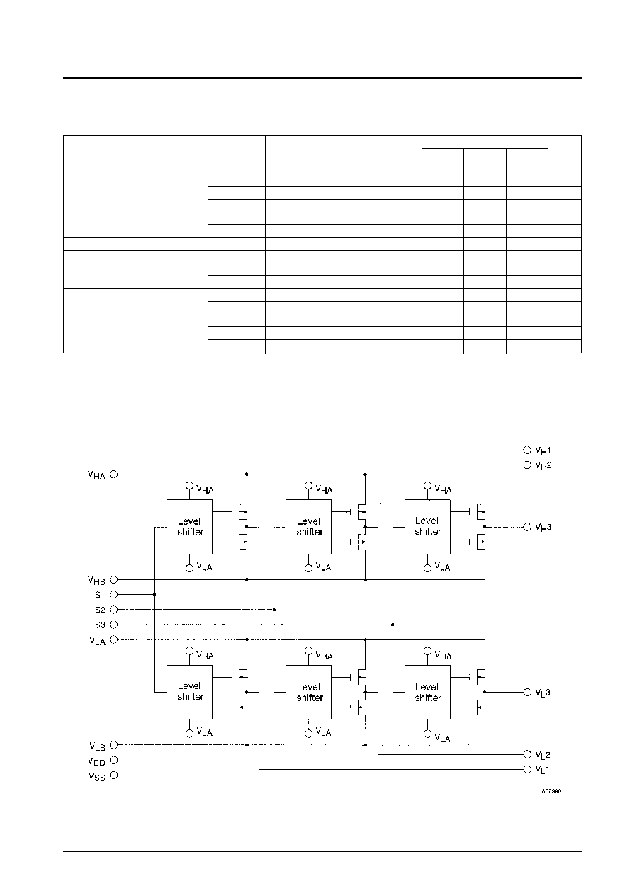
Block Diagram
No. 5912-3/4
LC4120NV
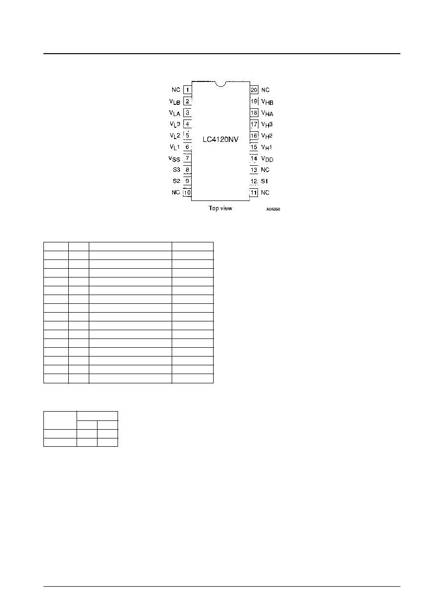
Pin Assignment
Pin Functions
Pin
I/O
Function
Signal voltage
V
H
1
O
High-voltage output 1
V
HA
/V
HB
V
H
2
O
High-voltage output 2
V
HA
/V
HB
V
H
3
O
High-voltage output 3
V
HA
/V
HB
V
L
1
O
Low-voltage output 1
V
LA
/V
LB
V
L
2
O
Low-voltage output 2
V
LA
/V
LB
V
L
3
O
Low-voltage output 3
V
LA
/V
LB
S1
I
Logic input 1
V
DD
/V
SS
S2
I
Logic input 2
V
DD
/V
SS
S3
I
Logic input 3
V
DD
/V
SS
V
HA
High-voltage power supply A
V
HB
High-voltage power supply B
V
LA
Low-voltage power supply A
V
LB
Low-voltage power supply B
V
DD
Logic system power supply
V
SS
Logic system ground
Truth Table
(n = 1, 2, 3)
Input signal
Output
Sn
V
Hn
V
Ln
H
V
HA
V
LA
L
V
HB
V
LB
PS No. 5912-4/4
LC4120NV
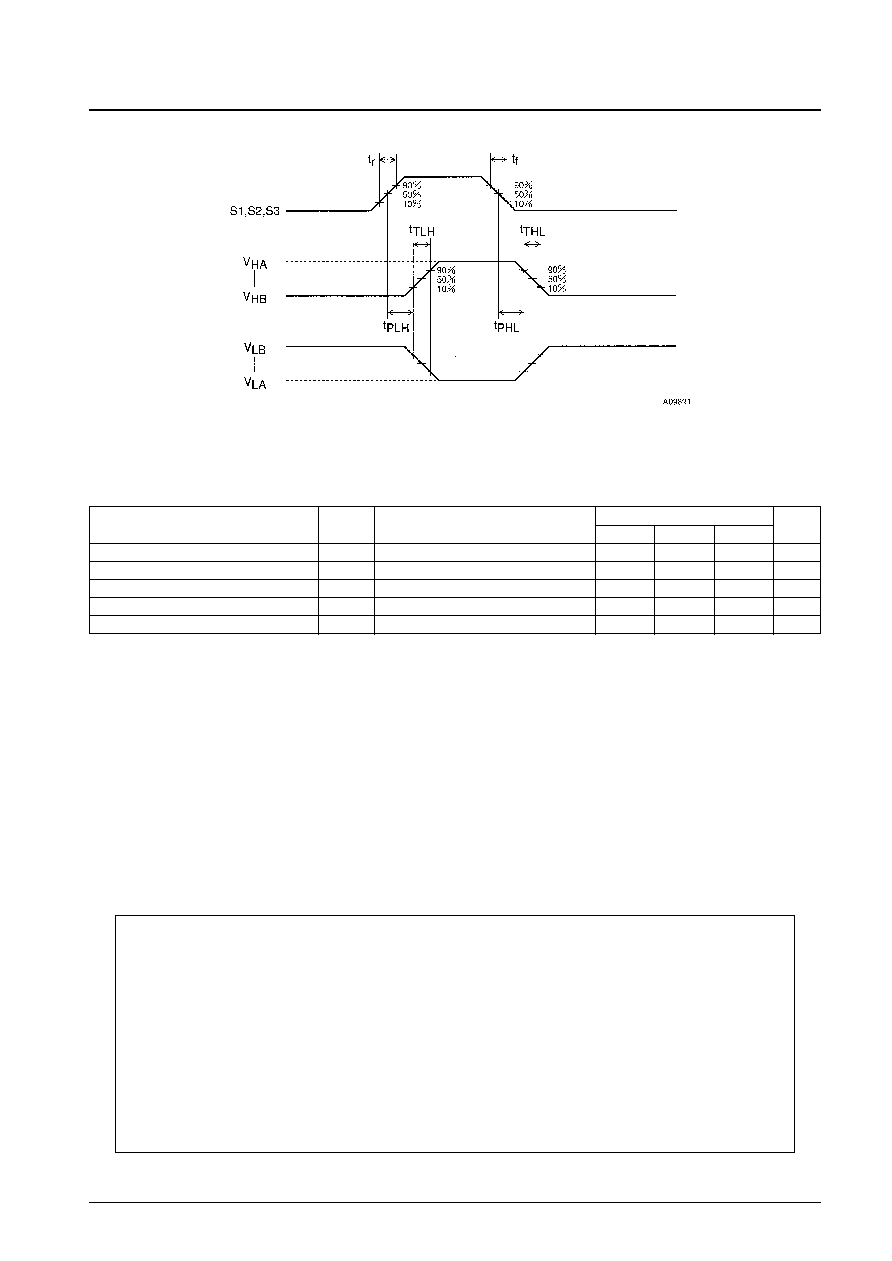
AC Characteristics
This catalog provides information as of March, 1998. Specifications and information herein are subject to
change without notice.
s
No products described or contained herein are intended for use in surgical implants, life-support systems, aerospace
equipment, nuclear power control systems, vehicles, disaster/crime-prevention equipment and the like, the failure of
which may directly or indirectly cause injury, death or property loss.
s
Anyone purchasing any products described or contained herein for an above-mentioned use shall:
Accept full responsibility and indemnify and defend SANYO ELECTRIC CO., LTD., its affiliates, subsidiaries and
distributors and all their officers and employees, jointly and severally, against any and all claims and litigation and all
damages, cost and expenses associated with such use:
Not impose any responsibility for any fault or negligence which may be cited in any such claim or litigation on
SANYO ELECTRIC CO., LTD., its affiliates, subsidiaries and distributors or any of their officers and employees
jointly or severally.
s
Information (including circuit diagrams and circuit parameters) herein is for example only; it is not guaranteed for
volume production. SANYO believes information herein is accurate and reliable, but no guarantees are made or implied
regarding its use or any infringements of intellectual property rights or other rights of third parties.
Parameter
Symbol
Conditions
Ratings
Unit
min
typ
max
Output rise time
t
TLH
80
160
ns
Output fall time
t
THL
80
160
ns
High-level transmission delay time
t
PLH
200
500
ns
Low-level transmission delay time
t
PHL
200
500
ns
Input rise and fall times
t
r
/t
f
30
ns
Conditions 1
at Ta = ≠20 to 75∞C, V
SS
= 0 V, V
DD
= 2.7 to 5.5 V, V
HA
= 42.5 V, V
HB
= 37.5 V, V
LA
= ≠37.5 V,
V
LB
= ≠32.5 V, C
L
= 50 pF,unless otherwise specified