 | –≠–ª–µ–∫—Ç—Ä–æ–Ω–Ω—ã–π –∫–æ–º–ø–æ–Ω–µ–Ω—Ç: LC4132C | –°–∫–∞—á–∞—Ç—å:  PDF PDF  ZIP ZIP |

Ordering number : ENN
*
6477
51200RM (OT) No. 6477-1/12
Overview
The LC4132C is a segment driver for large-scale dot
matrix LCDs. The LC4132C latches 240 bits of display
data sent from the controller (in 4- or 8-bit parallel units)
and generates the LCD drive signals. The LC4132C and
the LC4102C common driver form a chip set that can
drive a large-screen LCD panel.
Features
∑ CMOS (p-substrate) high voltage process
∑ LCD drive voltage: 36 V
∑ Logic system supply voltage: 2.7 to 5.5 V
∑ fcp max: 12 MHz (V
DD
= 5 V ±10%), 10 MHz (V
DD
=
2.7 to 4.5 V)
∑ Slim chip
∑ Can be switched between 4-bit an 8-bit parallel input.
∑ Output direction switching
∑ Display off function that holds the LCD drive voltages
at fixed levels.
∑ Display duty: 1/160 to 1/480
∑ Supports COG (chip on glass) mounting. (Gold bump
pads are used.)
LC4132C
SANYO Electric Co.,Ltd. Semiconductor Company
TOKYO OFFICE Tokyo Bldg., 1-10, 1 Chome, Ueno, Taito-ku, TOKYO, 110-8534 JAPAN
Dot Matrix STN LCD Segment Driver
CMOS IC
Any and all SANYO products described or contained herein do not have specifications that can handle
applications that require extremely high levels of reliability, such as life-support systems, aircraft's
control systems, or other applications whose failure can be reasonably expected to result in serious
physical and/or material damage. Consult with your SANYO representative nearest you before using
any SANYO products described or contained herein in such applications.
SANYO assumes no responsibility for equipment failures that result from using products at values that
exceed, even momentarily, rated values (such as maximum ratings, operating condition ranges, or other
parameters) listed in products specifications of any and all SANYO products described or contained
herein.
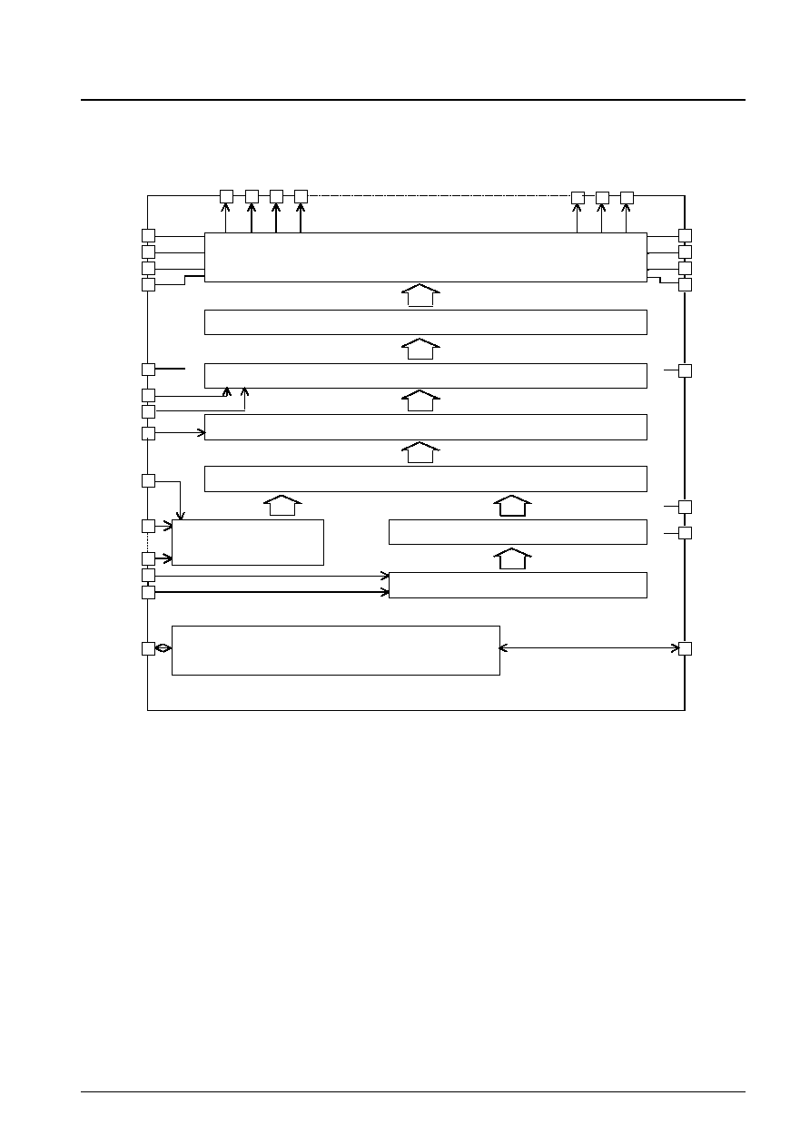
Block Diagram
No. 6477-2/12
LC4132C
O1
V0
V0
4 Level LCD Drive Circuit (240 bits)
Output Control
Level Shifter
2nd Latch (240 bits)
Bits Control
Address Decoder
Address Counter
Chip Disable & Latch Control
1st Latch (8 bits
◊
30)
V2
V3
V5
VDDH
VDD
VSS
EIO2
V2
V3
V5
VDDH
DISP
M
LOAD
BS
D0
to
D7
CP
R/L
EIO1
O2
O3
O4
O238
O239
O240
No. 6477-3/12
LC4132C
The electrical characteristics listed below apply when packaged in the Sanyo PGA-208 package.
Notes: 1. D0 to D7, LOAD, CP, R/L, DISP, M, EIO1, EIO2, BS
2. The following relationships must hold for V0, V2, V3, and V5: V
DDH
V0
V2
V
DDH
≠ 7 V, and 7 V
V3
V5
V
SS
.
Notes: 3. D0 to D7, LOAD, CP, R/L, M, DISP, BS, EIO1, EIO2
4. The following relationships must hold for V0, V2, V3, and V5: V
DDH
V0
V2
V
DDH
≠ 7 V, and 7 V
V3
V5
V
SS
.
At power on: The logic system power supply must be applied before the high-voltage system power supply. (Or they must both be applied at the
same time.)
At power off: The high-voltage system power supply must be turned off before the logic system power supply. (Or they must both be turned off at
the same time.)
Note: 5. The clock rise time (tr) and the clock fall time (tf) must meet the conditions (1) and (2) shown below.
1
---- ≠ tw (cph) ≠ tw (cpl)
fcp
(1) tr, tf < ------------------------
(2) tr, tf
50 ns
2
Parameter
Symbol
Conditions
Ratings
Unit
min
typ
max
V
DD
max
V
DD
≠0.3
7.0
V
Maximum supply voltage
V
DDH
max V
DDH
≠0.3
40.0
V
V
SS
max
V
SS
≠0.3
0.3
V
V
IN
*
1
≠0.3
V
DD
+ 0.3
V
Input voltage
V0, V2
V0, V2
*
2
V
DDH
≠ 7.0
V
DDH
+ 0.3
V
V3
V3
*
2
≠0.3
V
SS
+ 7.0
V
V5
V5
*
2
≠0.3
0.3
V
Operating temperature
Topr
≠20
+75
∞C
Storage temperature
Tstg
≠55
+125
∞C
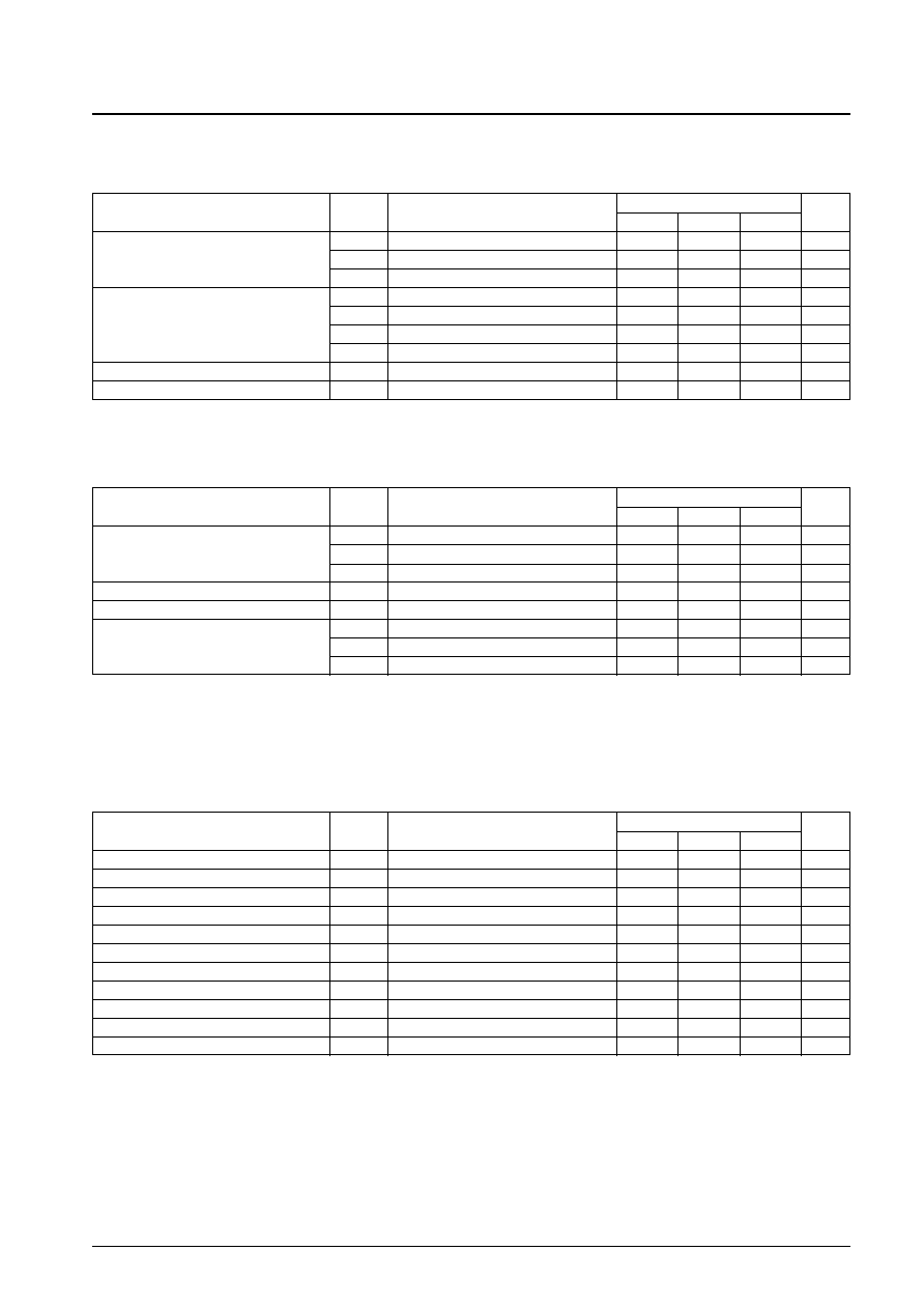
Absolute Maximum Ratings
at V
SS
= 0 V
Parameter
Symbol
Conditions
Ratings
Unit
min
typ
max
V
DD
V
DD
2.7
5.5
V
Supply voltage
V
DDH
V
DDH
20
36
V
V
SS
V
SS
0
V
Input high-level voltage
V
IH
*
3
0.8 V
DD
V
DD
V
Input low-level voltage
V
IL
*
3
0
0.2 V
DD
V
V0, V2
V0, V2
*
4
V
DDH
≠ 7.0
V
DDH
V
Input voltage
V3
V3
*
4
0
V
SSH
+ 7.0
V
V5
V5
*
1
0
V
Allowable Operating Ranges
at Ta = ≠20 to +75∞C, V
SS
= 0 V
Parameter
Symbol
Conditions
Ratings
Unit
min
typ
max
CP clock frequency
fcp
CP
12
MHz
High-level load pulse width
tw (ldH)
LOAD
50
ns
High-level clock pulse width
tw (cpH)
CP
20
ns
Low-level clock pulse width
tw (cpL)
CP
20
ns
LOAD/CP setup time
tsu (ld)
LOAD, CP
100
ns
LOAD/CP hold time
tho (ld)
LOAD, CP
200
ns
DATA/CP setup time
tsu (cp)
CP, D0 to D7
10
ns
DATA/CP hold time
tho (cp)
CP, D0 to D7
10
ns
EIO input setup time
tsu (ei)
CP, EIO1, EIO2
24
ns
Clock rise time
tr
LOAD, CP
*
5
50
ns
Clock fall time
tf
LOAD, CP
*
5
50
ns
V
DD
= 5 V ±10%, Ta = ≠20 to +75∞C, V
SS
= 0 V
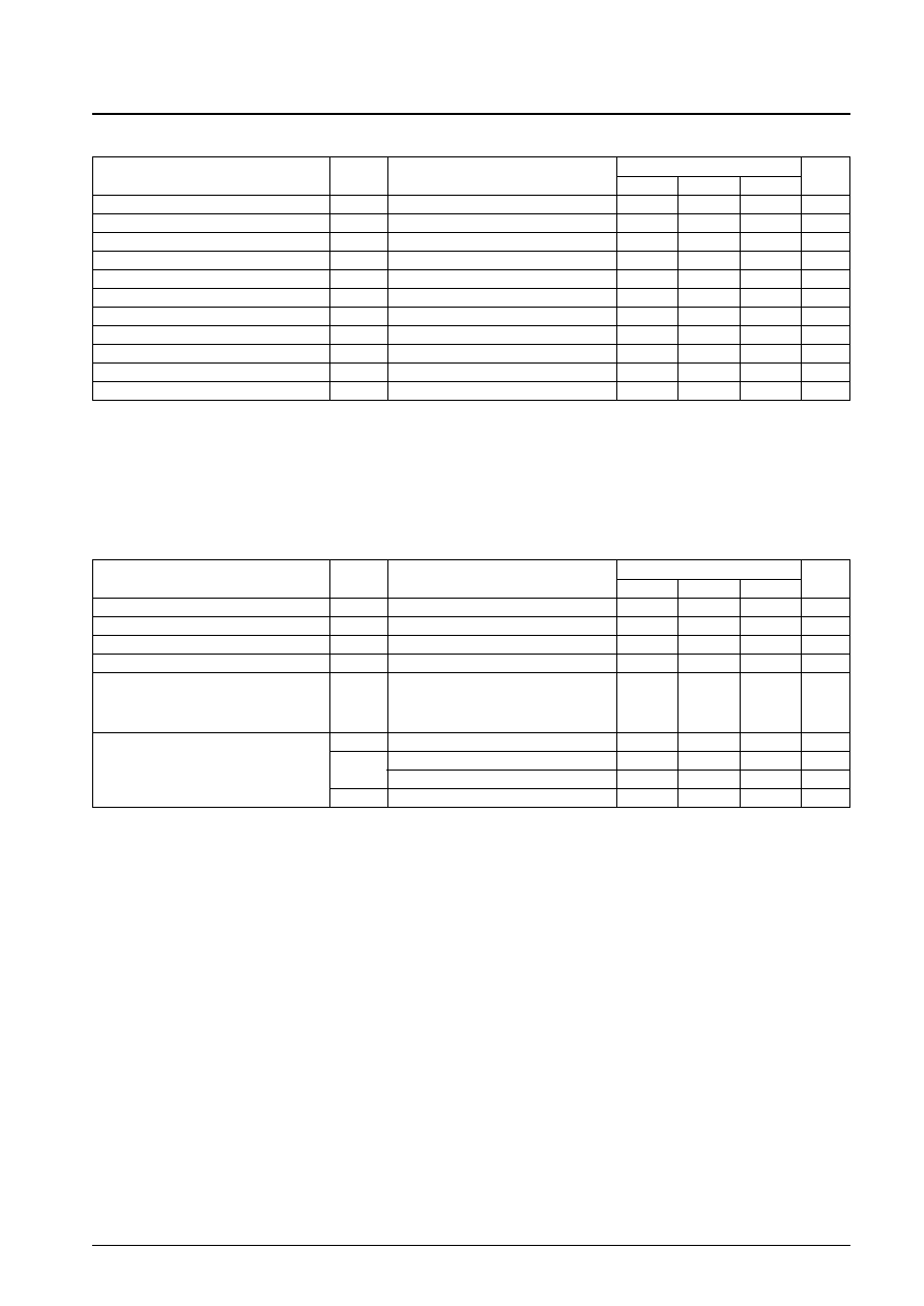
No. 6477-4/12
LC4132C
Note: 6. The clock rise time (tr) and the clock fall time (tf) must meet the conditions (1) and (2) shown below.
1
---- ≠ tw (cph) ≠ tw (cpl)
fcp
(1) tr, tf < ------------------------
(2) tr, tf
50 ns
2
Parameter
Symbol
Conditions
Ratings
Unit
min
typ
max
CP clock frequency
fcp
CP
10
MHz
High-level load pulse width
tw (ldH)
LOAD
50
ns
High-level clock pulse width
tw (cpH)
CP
37
ns
Low-level clock pulse width
tw (cpL)
CP
37
ns
LOAD/CP setup time
tsu (ld)
LOAD, CP
100
ns
LOAD/CP hold time
tho (ld)
LOAD, CP
350
ns
DATA/CP setup time
tsu (cp)
CP, D0 to D7
35
ns
DATA/CP hold time
tho (cp)
CP, D0 to D7
35
ns
EIO input setup time
tsu (ei)
CP, EIO1, EIO2
30
ns
Clock rise time
tr
LOAD, CP
*
6
50
ns
Clock fall time
tf
LOAD, CP
*
6
50
ns
V
DD
= 2.7 to 4.5 V, Ta = ≠20 to +75∞C, V
SS
= 0 V
Notes: 7. D0 to D7, LOAD, CP, R/L, M, DISP, EIO1, 2, BS
8. V
O
is the voltage applied by an on-state output, V0 = V
DDH
, V2 = 18/20 (V
DDH
≠ V
SS
), V3 = 2/20 (V
DDH
≠ V
SS
), V5 = V
SS
.
9. Measured when either LOAD = 28 kHz, CP = 10 MHz, and M = 75 Hz, or with no load and input at V
IH
= V
DD
or V
IL
= V
SS
.
10. The current drain in standby mode. Or when EIOn (input) = V
DD
.
Parameter
Symbol
Conditions
Ratings
Unit
min
typ
max
Input high-level voltage
I
IH
V
IN
= V
DD
*
7
5
µA
Input low-level voltage
I
IL
1
V
IN
= V
SS
*
7
≠5
µA
Output high-level voltage
V
OH
I
O
= ≠0.4 mA: EIO1, EIO2
V
DD
≠ 0.4
V
DD
V
Output low-level voltage
V
OL
I
O
= 0.4 mA: EIO1, EIO2
V
SS
0.4
V
V
DDH
= 36 V
*
8
Output on resistance
R
OUT
V0 ≠ V
O
= 0.5 V, V2 ≠ V
O
= 0.5 V
1
3
k
V
O
≠ V3 = 0.5 V, V
O
≠ V5 = 0.5 V
: O1 to O240
I
DD
V
DD
= 2.7 to 5.5 V
5.0
mA
Current drain
I
DDH
V
DD
= 2.7 to 5.5 V, V
DDH
= 32 V
*
9
3.0
mA
V
DD
= 5 V ±10%, V
DDH
= 36 V
3.0
mA
I
ST
*
10
500
µA
Electrical Characteristics at Ta = ≠20 to +75∞C, V
DD
= 2.7 to 5.5 V, V
SS
= 0 V
No. 6477-5/12
LC4132C
Parameter
Symbol
Conditions
Ratings
Unit
min
typ
max
EIO output delay time
td (eo)
30 pF capacitance load: CP, EIO1, EIO2
40
ns
LOAD/EIO output delay time
td (leo)
30 pF capacitance load: LOAD, EIO1, EIO2
70
ns
LOAD/On delay time
td (ldo)
100 pF capacitance load: LOAD, O1 to O240
700
ns
M/On delay time
td (mo)
100 pF capacitance load: M, O1 to O240
700
ns
Switching Characteristics
at Ta = ≠20 to +75∞C, V
SS
= 0 V
Parameter
Symbol
Conditions
Ratings
Unit
min
typ
max
EIO output delay time
td (eo)
30 pF capacitance load: CP, EIO1, EIO2
80
ns
LOAD/EIO output delay time
td (leo)
30 pF capacitance load: LOAD, EIO1, EIO2
130
ns
LOAD/On delay time
td (ldo)
100 pF capacitance load: LOAD, O1 to O240
3
µs
M/On delay time
td (mo)
100 pF capacitance load: M, O1 to O240
3
µs
V
DD
= 2.5 to 4.5 V
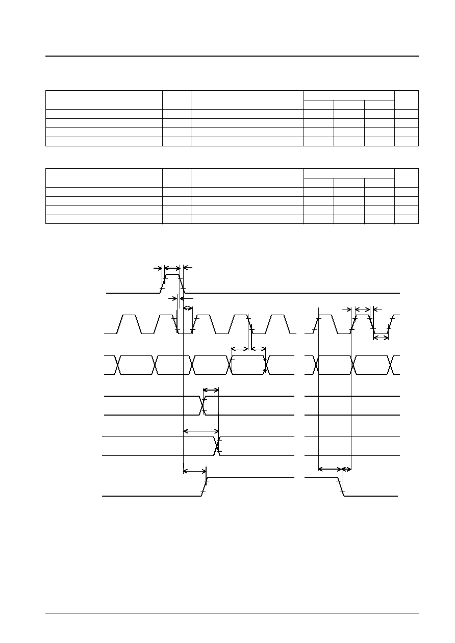
Timing Chart
(V
IH
= 0.8 V
DD
, V
IL
= 0.2 V
DD
)
0.2VDD
0.8VDD
tr(ld)
tw(ldH)
tf(ld)
tho(ld)
tsu(ld)
td(mo)
tsu(cp)
tho(cp)
td(leo)
tr(cp)
tw(cpH)
tf(cp)
tw(cpL)
td(eo)
tsu(ei)
td(ldo)
EIOn (output)
(input to the next stage)
V
DD
= 5 V ±10%
LOAD
CP
D0 to D7
M
On