 | –≠–ª–µ–∫—Ç—Ä–æ–Ω–Ω—ã–π –∫–æ–º–ø–æ–Ω–µ–Ω—Ç: LC4966 | –°–∫–∞—á–∞—Ç—å:  PDF PDF  ZIP ZIP |

Overview
The LC4966 is an IC that provides the same functions as
the MLC4066B and the MLC4066BH over an expanded
usable voltage range. The LC4966 provides four
bidirectional switch circuits. These circuits form a low-
impedance conducting path between the input and output
sides when the corresponding control input (CONT) is set
high, and form a high-impedance nonconducting open
circuit when the control input is set low.
Package Dimensions
unit: mm
3003A-DIP14
CMOS LSI
42696HA (OT) No. 1536-1/6
SANYO: DIP14
[LC4966]
SANYO Electric Co.,Ltd. Semiconductor Bussiness Headquarters
TOKYO OFFICE Tokyo Bldg., 1-10, 1 Chome, Ueno, Taito-ku, TOKYO, 110 JAPAN
Quad Bilateral Switch
LC4966
Ordering number : EN1536B
Specifications
Absolute Maximum Ratings
at Ta = 25∞C, V
SS
= 0 V
Allowable Operating Ranges
at Ta = ≠40 to +85∞C
Parameter
Symbol
Conditions
Ratings
Unit
Maximum supply voltage
V
DD
max
V
SS
≠ 0.5 to V
SS
+ 40
V
Input voltage
V
IN
V
SS
≠ 0.5 to V
DD
+ 0.5
V
Output voltage
V
OUT
V
SS
≠ 0.5 to V
DD
+ 0.5
V
Input current
I
IN
±10
mA
Potential difference between input and
V
I
-V
O
±0.5
V
output when on
Lead soldering temperature time
T
sol
t = 10 s
260
∞C
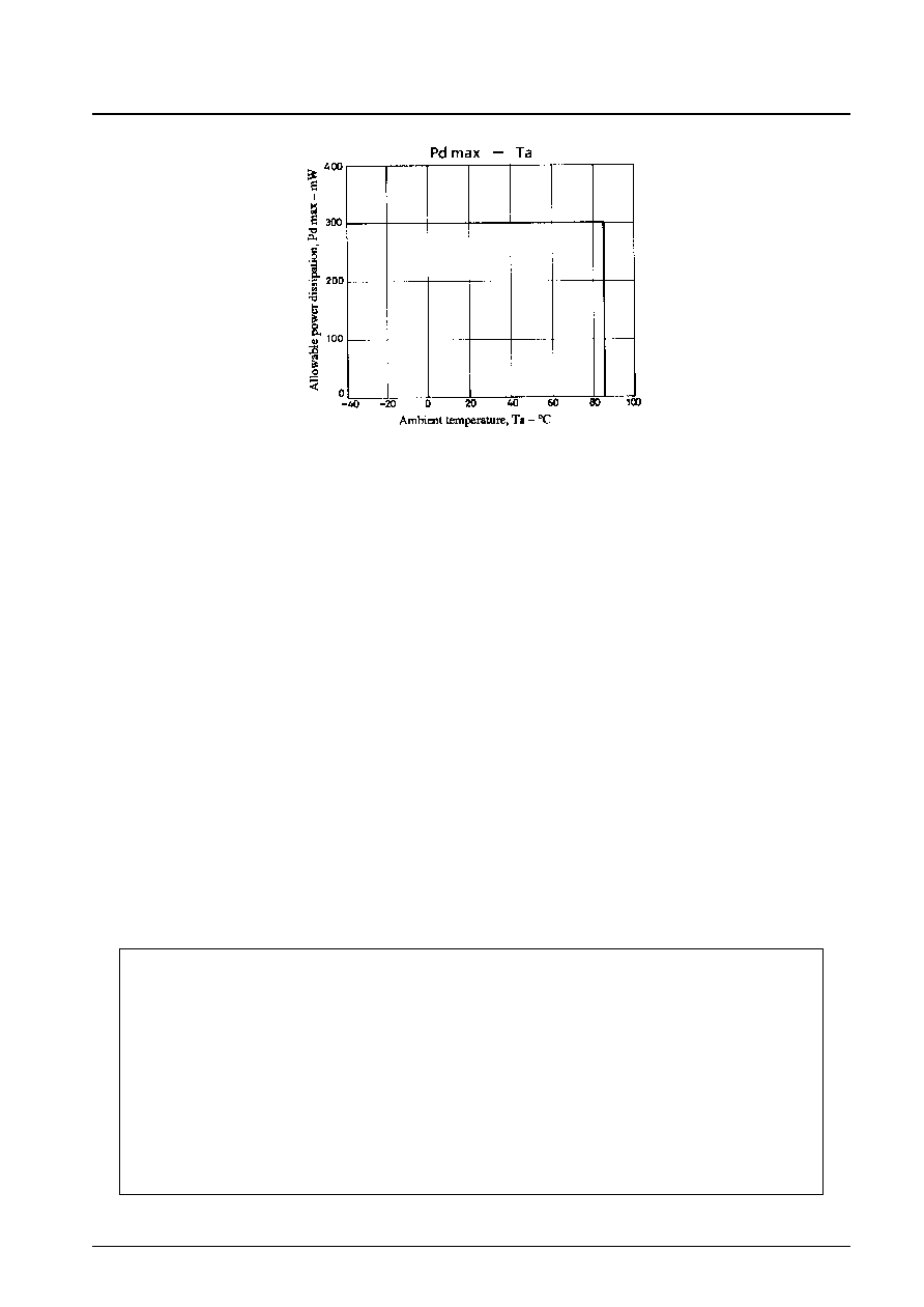
Allowable power dissipation
Pd max
Ta
85∞C, I
IN
= ±10 mA
300
mW
Operating temperature
Topr
≠40 to +85
∞C
Storage temperature
Tstg
≠65 to +150
∞C
Parameter
Symbol
Conditions
Ratings
Unit
Supply voltage
V
DD
3 to 37
V
Input voltage
V
IN
0 to V
DD
V
No. 1536-2/6
LC4966
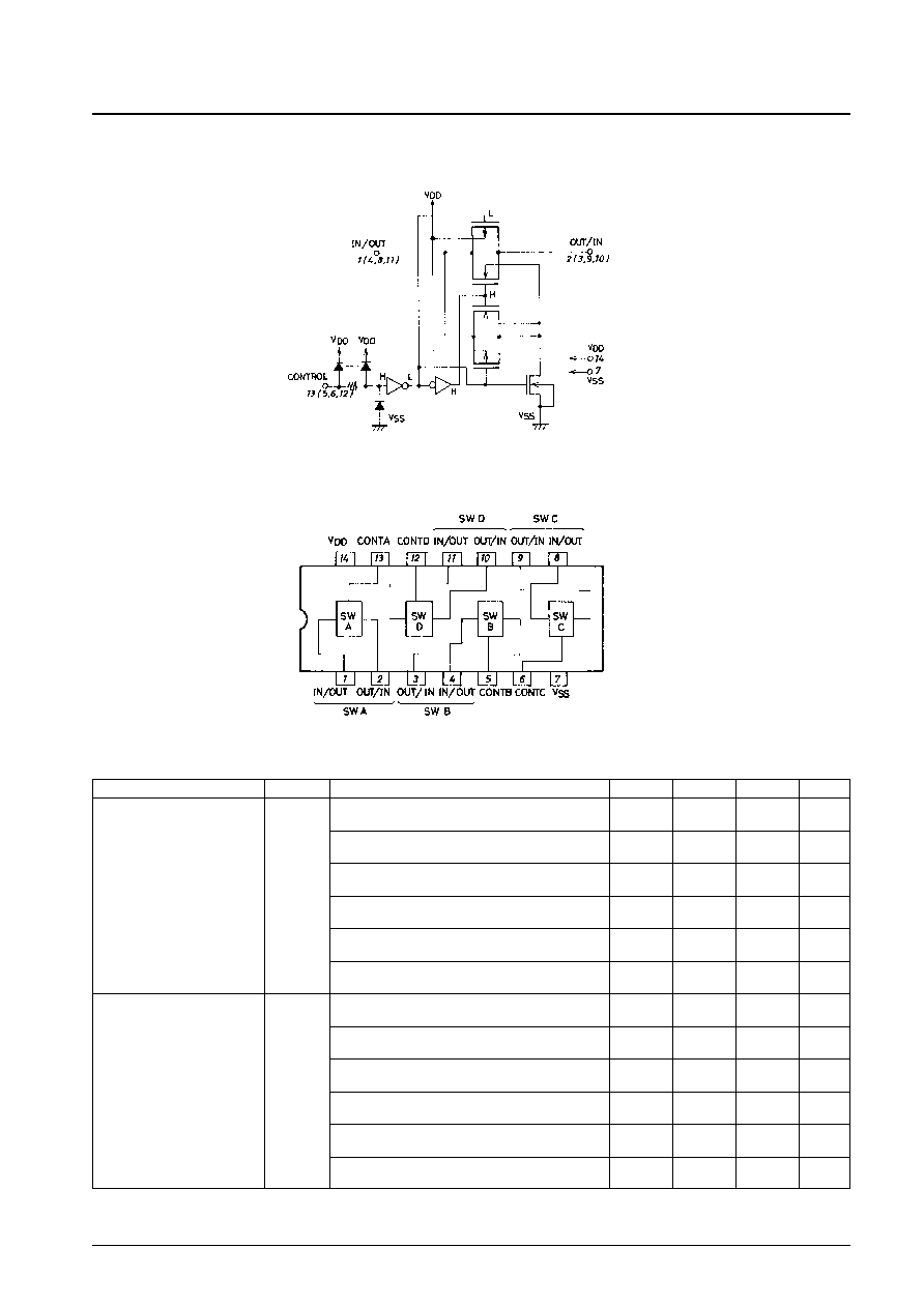
Equivalent Circuit
(1/4 LC4966)
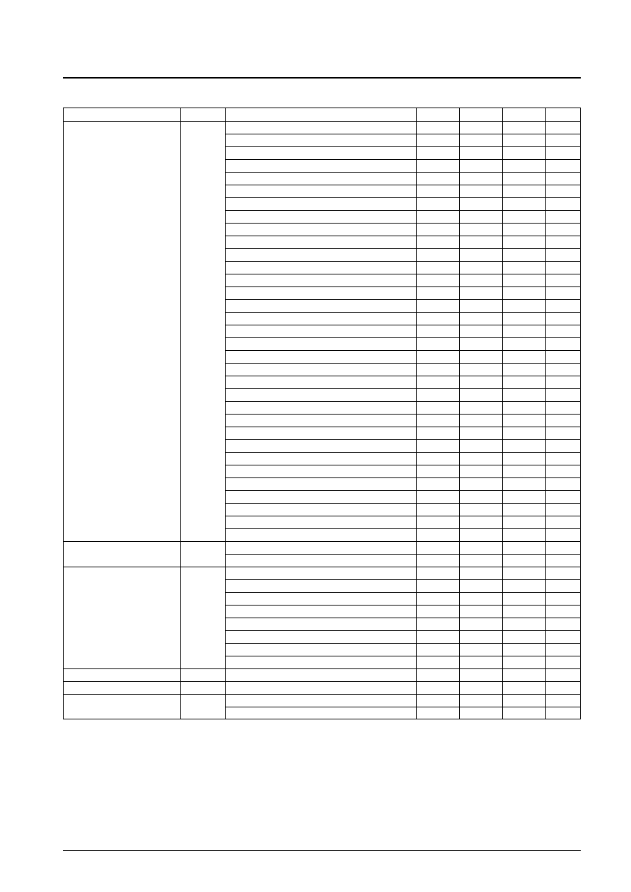
Pin Assignment and Equivalent Circuit Block Diagram
Electrical Characteristics
at Ta = 25 ± 2∞C, V
SS
= 0 V
Parameter
Symbol
Conditions
min
typ
max
Unit
V
DD
= 5 V,
3.5
V
for a current between input and output > 10 µA
V
DD
= 10 V,
8.0
V
for a current between input and output > 10 µA
V
DD
= 15 V,
12.5
V
Input high-level control voltage
V
IH
for a current between input and output > 10 µA
V
DD
= 20 V,
17.0
V
for a current between input and output > 10 µA
V
DD
= 30 V,
27.0
V
for a current between input and output > 10 µA
V
DD
= 37 V,
34.0
V
for a current between input and output > 10 µA
V
DD
= 5 V,
1.0
V
for a current between input and output < 10 µA
V
DD
= 10 V,
2.0
V
for a current between input and output < 10 µA
V
DD
= 15 V,
2.5
V
Input low-level control voltage
V
IL
for a current between input and output < 10 µA
V
DD
= 20 V,
2.5
V
for a current between input and output < 10 µA
V
DD
= 30 V,
3.0
V
for a current between input and output < 10 µA
V
DD
= 37 V,
3.0
V
for a current between input and output < 10 µA
Continued on next page.
No. 1536-3/6
LC4966
Continued from preceding page.
Parameter
Symbol
Conditions
min
typ
max
Unit
V
DD
= 5 V, V
IN
= 5 V, I = ±1 mA
110
220
V
DD
= 5 V, V
IN
= 2.5 V, I = ±1 mA
90
180
V
DD
= 5 V, V
IN
= 0.25 V, I = ±1 mA
110
220
V
DD
= 10 V, V
IN
= 10 V, I = ±3 mA
70
140
V
DD
= 10 V, V
IN
= 5 V, I = ±3 mA
50
100
V
DD
= 10 V, V
IN
= 0.25 V, I = ±3 mA
70
140
V
DD
= 15 V, V
IN
= 15 V, I = ±3 mA
60
120
V
DD
= 15 V, V
IN
= 7.5 V, I = ±3 mA
40
80
V
DD
= 15 V, V
IN
= 0.25 V, I = ±3 mA
60
120
V
DD
= 20 V, V
IN
= 20 V, I = ±3 mA
60
120
V
DD
= 20 V, V
IN
= 10 V, I = ±3 mA
40
80
V
DD
= 20 V, V
IN
= 0.25 V, I = ±3 mA
60
120
V
DD
= 30 V, V
IN
= 30 V, I = ±3 mA
50
100
V
DD
= 30 V, V
IN
= 15 V, I = ±3 mA
35
70
V
DD
= 30 V, V
IN
= 0.25 V, I = ±3 mA
50
100
V
DD
= 37 V, V
IN
= 37 V, I = ±3 mA
45
90
On resistance
R
ON
V
DD
= 37 V, V
IN
= 19 V, I = ±3 mA
30
60
V
DD
= 37 V, V
IN
= 0.25 V, I = ±3 mA
45
90
V
DD
= +5 V, V
IN
= ≠5 V, V
IN
= 5 V, I = ±3 mA
70
140
V
DD
= +5 V, V
SS
= ≠5 V, V
IN
= ±0.25 V, I = ±3 mA
50
100
V
DD
= +5 V, V
SS
= ≠5 V, V
IN
= ≠5 V, I = ±3 mA
70
140
V
DD
= +7.5 V, V
SS
= ≠7.5 V, V
IN
= 5 V, I = ±3 mA
60
120
V
DD
= +7.5 V, V
SS
= ≠7.5 V, V
IN
= ±0.25 V, I = ±3 mA
40
80
V
DD
= +7.5 V, V
SS
= ≠7.5 V, V
IN
= ≠5 V, I = ±3 mA
60
120
V
DD
= +10 V, V
SS
= ≠10 V, V
IN
= 10 V, I = ±3 mA
60
120
V
DD
= +10 V, V
SS
= ≠10 V, V
IN
= ±0.25 V, I = ±3 mA
40
80
V
DD
= +10 V, V
SS
= ≠10 V, V
IN
= ≠10 V, I = ±3 mA
60
120
V
DD
= +15 V, V
SS
= ≠15 V, V
IN
= 15 V, I = ±3 mA
50
100
V
DD
= +15 V, V
SS
= ≠15 V, V
IN
= ±0.25 V, I = ±3 mA
35
70
V
DD
= +15 V, V
SS
= ≠15 V, V
IN
= ≠15 V, I = ±3 mA
50
100
V
DD
= +18.5 V, V
SS
= ≠18.5 V, V
IN
= 18.5 V, I = ±3 mA
45
90
V
DD
= +18.5 V, V
SS
= ≠18.5 V, V
IN
= ±0.25 V, I = ±3 mA
30
60
V
DD
= +18.5 V, V
SS
= ≠18.5 V, V
IN
= ≠18.5 V, I = ±3 mA
45
90
Input off leakage current
I
OFF
V
DD
= 37 V, V
IN
= 37 V, V
OUT
= 0 V
±1
±500
nA
V
DD
= 37 V, V
IN
= 0 V, V
OUT
= 37 V
±1
±500
nA
V
DD
= 5 V
0.001
1
µA
V
DD
= 10 V
0.001
2
µA
V
DD
= 15 V
0.002
4
µA
Quiescent current drain
I
DD
V
DD
= 20 V
0.004
8
µA
V
DD
= 25 V
0.01
20
µA
V
DD
= 30 V
0.02
40
µA
V
DD
= 35 V
0.04
80
µA
V
DD
= 37 V
0.1
160
µA
Input high-level control current
I
IH
V
DD
= 37 V, V
IN
= 37 V
10
≠4
3
µA
Input low-level control current
I
IL
V
DD
= 37 V, V
IN
= 0 V
≠10
≠4
3
µA
Input capacitance
C
IN
Control inputs
5
7.5
pF
Switch input and outputs
10
pF
No. 1536-4/6
LC4966
Switching Characteristics
at Ta = 25 ± 2∞C
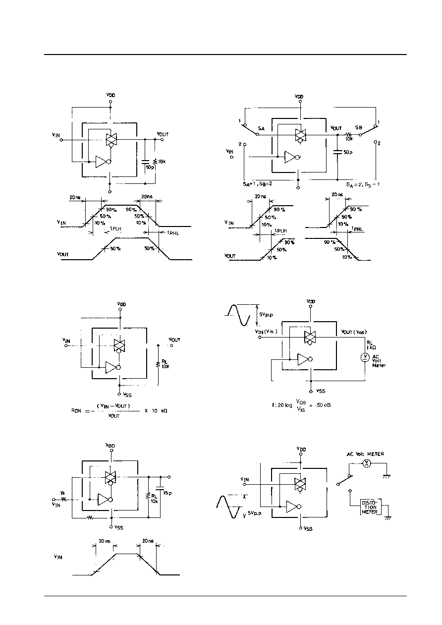
Note 1. Vis is a ±2.5 Vp-p sine wave; fmax: 20log (Vos/Vis) = the ≠3 dB frequency.
2. Vis is a ±2.5 Vp-p sine wave.
3. Vis is a ±2.5 Vp-p sine wave. Frequency (feedthrough): 20log(Vos/Vis) = ≠50 dB
Parameter
Symbol
Conditions
min
typ
max
Unit
V
DD
= 5 V, R
L
= 10 k
, C
L
= 50 pF
15
45
ns
V
DD
= 10 V, R
L
= 10 k
, C
L
= 50 pF
10
30
ns
V
DD
= 15 V, R
L
= 10 k
, C
L
= 50 pF
8
25
ns
Transmission time (IN to OUT)
t
PLH
, t
PHL
V
DD
= 20 V, R
L
= 10 k
, C
L
= 50 pF
8
25
ns
V
DD
= 25 V, R
L
= 10 k
, C
L
= 50 pF
8
25
ns
V
DD
= 30 V, R
L
= 10 k
, C
L
= 50 pF
7
25
ns
V
DD
= 35 V, R
L
= 10 k
, C
L
= 50 pF
7
25
ns
V
DD
= 37 V, R
L
= 10 k
, C
L
= 50 pF
7
25
ns
V
DD
= 5 V, R
L
= 10 k
, C
L
= 50 pF
100
200
ns
V
DD
= 10 V, R
L
= 10 k
, C
L
= 50 pF
40
70
ns
V
DD
= 15 V, R
L
= 10 k
, C
L
= 50 pF
35
60
ns
Transmission time
t
PLH
, t
PHL
V
DD
= 20 V, R
L
= 10 k
, C
L
= 50 pF
35
60
ns
(control
OUT)
V
DD
= 25 V, R
L
= 10 k
, C
L
= 50 pF
35
60
ns
V
DD
= 30 V, R
L
= 10 k
, C
L
= 50 pF
35
60
ns
V
DD
= 35 V, R
L
= 10 k
, C
L
= 50 pF
35
60
ns
V
DD
= 37 V, R
L
= 10 k
, C
L
= 50 pF
35
60
ns
V
DD
= 5 V, C
L
= 15 pF
1.0
MHz
V
DD
= 10 V, C
L
= 15 pF
1.0
MHz
Maximum control input frequency
f max (c)
V
DD
= 20 V, C
L
= 15 pF
1.0
MHz
V
DD
= 30 V, C
L
= 15 pF
1.0
MHz
V
DD
= 37 V, C
L
= 15 pF
1.0
MHz
V
DD
= +5 V, V
SS
= ≠5 V, R
L
= 10 k
, C
L
= 15 pF
*
1
35
MHz
Maximum transmission frequency
f max (I-O)
V
DD
= +10 V, V
SS
= ≠10 V
40
MHz
V
DD
= +15 V, V
SS
= ≠15 V
50
MHz
V
DD
= +18.5 V, V
SS
= ≠18.5 V
50
MHz
V
DD
= +5 V, V
SS
= ≠5 V, R
L
= 10 k
, f = 1 kHz
*
2
0.010
%
Sine wave total harmonic
V
DD
= +10 V, V
SS
= ≠10 V
0.005
%
distortion
V
DD
= +15 V, V
SS
= ≠15 V
0.005
%
V
DD
= +18.5 V, V
SS
= ≠18.5 V
0.005
%
V
DD
= +5 V, V
SS
= ≠5 V, R
L
= 10 k
*
3
1
MHz
Feedthrough (switch off state)
V
DD
= +10 V, V
SS
= ≠10 V
1
MHz
V
DD
= +15 V, V
SS
= ≠15 V
1
MHz
V
DD
= +18.5 V, V
SS
= ≠18.5 V
1
MHz
No. 1536-5/6
LC4966
Test Circuits and Waveforms
Unit (resistance:
, capacitance: F)
1. t
PLH
, t
PHL
(IN-OUT) Test Circuit
2. t
PLH
, t
PHL
(Control-OUT) Test Circuit
3. R
ON
Test Circuit
4. Feedthrough Test Circuit
5. Crosstalk
6. Frequency Response (f max) and Total Harmonic Distortion
No. 1536-6/6
LC4966
This catalog provides information as of December, 1997. Specifications and information herein are subject to
change without notice.
s
No products described or contained herein are intended for use in surgical implants, life-support systems, aerospace
equipment, nuclear power control systems, vehicles, disaster/crime-prevention equipment and the like, the failure of
which may directly or indirectly cause injury, death or property loss.
s
Anyone purchasing any products described or contained herein for an above-mentioned use shall:
Accept full responsibility and indemnify and defend SANYO ELECTRIC CO., LTD., its affiliates, subsidiaries and
distributors and all their officers and employees, jointly and severally, against any and all claims and litigation and all
damages, cost and expenses associated with such use:
Not impose any responsibility for any fault or negligence which may be cited in any such claim or litigation on
SANYO ELECTRIC CO., LTD., its affiliates, subsidiaries and distributors or any of their officers and employees
jointly or severally.
s
Information (including circuit diagrams and circuit parameters) herein is for example only; it is not guaranteed for
volume production. SANYO believes information herein is accurate and reliable, but no guarantees are made or implied
regarding its use or any infringements of intellectual property rights or other rights of third parties.