 | –≠–ª–µ–∫—Ç—Ä–æ–Ω–Ω—ã–π –∫–æ–º–ø–æ–Ω–µ–Ω—Ç: LC573102A | –°–∫–∞—á–∞—Ç—å:  PDF PDF  ZIP ZIP |
Any and all SANYO products described or contained herein do not have specifications that can handle
applications that require extremely high levels of reliability, such as life-support systems, aircraft's
control systems, or other applications whose failure can be reasonably expected to result in serious
physical and/or material damage. Consult with your SANYO representative nearest you before using
any SANYO products described or contained herein in such applications.
SANYO assumes no responsibility for equipment failures that result from using products at values that
exceed, even momentarily, rated values (such as maximum ratings, operating condition ranges,or other
parameters) listed in products specifications of any and all SANYO products described or contained
herein.
CMOS IC
4-bit Single Chip Microcontroller
Ordering number:ENN
*
4144
LC573104A, 573102A
SANYO Electric Co.,Ltd. Semiconductor Company
TOKYO OFFICE Tokyo Bldg., 1-10, 1 Chome, Ueno, Taito-ku, TOKYO, 110-8534 JAPAN
O1501TN (KT)/13195JN/5252JN No.4144≠1/16
1
12
24
13
12.5
(0.75)
1.0
0.15
0.35
5.4
7.6
0.63
1.7max
1.5
0.1
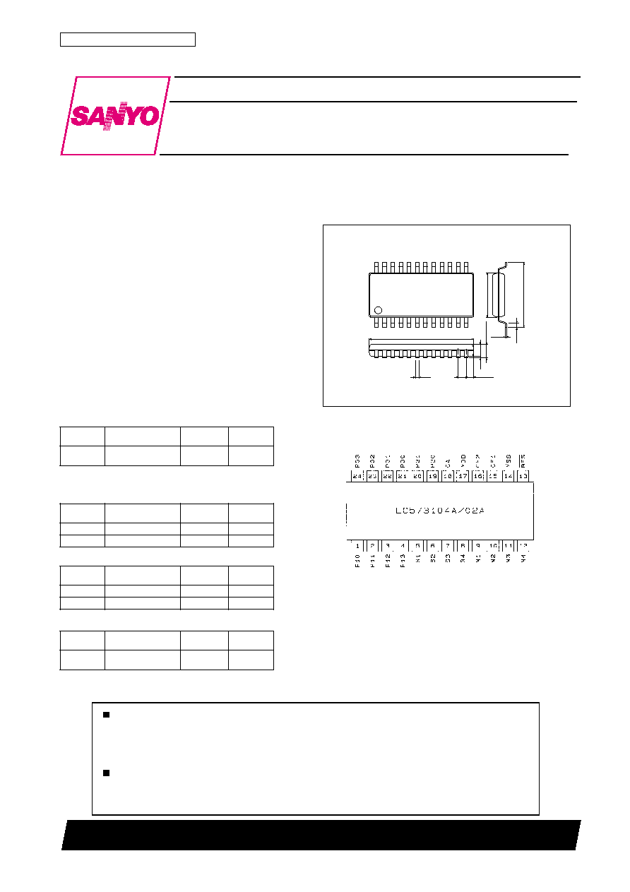
Package Dimensions
unit:mm
3112A-MFP24S
[LC573104A, 573102A]
SANYO : MFP24S
Preliminary
Overview
L C 5 7 3 1 0 4 A a n d L C 5 7 3 1 0 2 A a r e C M O S 4 - b i t
microcontrollers featuring low-voltage operation and low
power dissipation.
Both LC573104A and LC573102A incorporate a 4-bit par-
allel processing ALU, 4K bytes/2K bytes ROM, a 64
◊
4-bit
RAM, a 16-bit timer, and an infrared remote control trans-
mission carrier output circuit.
Applications
∑ Remote controller.
∑ Control of small measuring instruments.
Features
∑ ROM : 4096
◊
8 bits (LC573104A)
2048
◊
8 bits (LC573102A)
∑ RAM : 64
◊
4 bits
∑ Cycle time
∑ Current Drain
a. At normal operation
b. HALT mode
c. HOLD mode
e
l
c
y
C
e
m
i
t
k
c
o
l
c
m
e
t
s
y
S
r
o
t
a
r
e
n
e
g
n
o
i
t
a
ll
i
c
s
O
y
c
n
e
u
q
e
r
f
y
l
p
p
u
S
e
g
a
t
l
o
v
s
µ
6
.
7
1
n
o
i
t
a
ll
i
c
s
o
c
i
m
a
r
e
C
t
i
u
c
r
i
c
z
H
k
5
5
4
V
0
.
6
o
t
3
.
2
t
n
e
r
r
u
C
n
i
a
r
d
k
c
o
l
c
m
e
t
s
y
S
r
o
t
a
r
e
n
e
g
n
o
i
t
a
ll
i
c
s
O
y
c
n
e
u
q
e
r
f
y
l
p
p
u
S
e
g
a
t
l
o
v
p
y
t
A
µ
0
5
1
n
o
i
t
a
ll
i
c
s
o
R
C
z
H
k
5
5
4
V
0
.
3
p
y
t
A
µ
0
0
4
n
o
i
t
a
ll
i
c
s
o
R
C
z
H
k
5
5
4
V
0
.
5
t
n
e
r
r
u
C
n
i
a
r
d
k
c
o
l
c
m
e
t
s
y
S
r
o
t
a
r
e
n
e
g
n
o
i
t
a
ll
i
c
s
O
y
c
n
e
u
q
e
r
f
y
l
p
p
u
S
e
g
a
t
l
o
v
p
y
t
A
µ
0
8
n
o
i
t
a
ll
i
c
s
o
R
C
z
H
k
5
5
4
V
0
.
3
p
y
t
A
µ
0
0
3
n
o
i
t
a
ll
i
c
s
o
R
C
z
H
k
5
5
4
V
0
.
5
e
g
a
k
a
e
L
t
n
e
r
r
u
c
n
o
i
t
i
d
n
o
C
n
o
i
t
a
ll
i
c
s
O
y
c
n
e
u
q
e
r
f
y
l
p
p
u
S
e
g
a
t
l
o
v
p
y
t
A
µ
1
.
0
n
o
i
t
a
ll
i
c
s
o
R
C
n
e
h
W
e
d
o
m
P
O
T
S
t
a
s
i
z
H
k
5
5
4
V
0
.
5
Pin Assignment

LC573104A, 573102A
No.4144≠2/16
∑ Port
∑ Input port (S port, M port) :
2-port (8 pins)
[Key scan input port]
∑ Input/Ouput port :
3-port (10 pins)
P0 port, P1 port
2-port (8 pins)
[Key scan output port]
P2 port
1-port (2 pins)
[Key scan expansion port]
[LED direct drivable port]
∑ Infrared remote control carrier generation circuit.
∑ Software-controllable remote control carrier output ON/OFF.
∑ Software-controllable carrier frequency and duty ratio.
<38kHz-1/3 duty, 38kHz-1/2 duty, 57kHz-1/2 duty>
(When fixed carrier signal is output, it is specified by mask option)
∑ 1kHz to 200kHz infrared remote control transmission carrier frequency.
(When carrier output is selected by timer at mask option, and when 455kHz CR oscillator is used)
∑ Infrared carrier output-dedicated terminal built-in (CA terminal).
∑ 108ms HALT-mode cancel signal output.
∑ Timer
∑ 16-bit software-controllable Timer
Timer input clock : Ceramic (CR) oscillation frequency (455kHz).
∑ 108ms HALT release request signal generation timer (Free running timer).
∑ Watchdog timer (changed over between USED/UNUSED by mask option)
∑ Sub-routine stack level
∑ 2 levels
∑ Oscillation circuit
∑ Ceramic (CR) oscillation circuit : 455kHz (for System clock generation), Feedback resistor built-in.
∑ Standby function
∑ HALT mode
HALT mode used to reduce current drain.
HALT mode suspends program execution.
Following shows how to release the HALT mode.
(A) System reset
(B) HALT mode release request signal.
∑ HOLD mode
HOLD mode stops ceramic resonator (CR). The HOLD mold can be released in two ways.
(A) System reset
(B) Apply H level input to S port pin or M port pin. (However, it is necessary to set S port or M port HOLD mode
release permission flag beforehand.)
∑ From of shipment
∑ MFP-24S (1.0mm pitch) and chip.
NOTE : When dipping in solder to mount the MFP package on board, contact SANYO for instructions.
LC573104A, 573102A
No.4144≠3/16
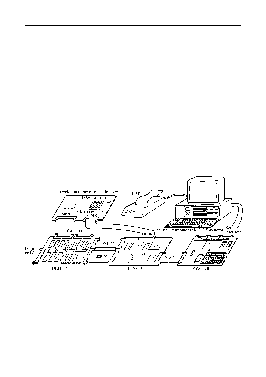
The Application Development System for the LC573100 Series.
(1) Manual
(A) Users Manual : LC573100 Series Users Manual.
(B) Development Tool Manual : LC573100 Series Development Tool Manual.
(2) Development Tools
∑ Tools for application development of the LC573100 Series.
(A) Personal computer (MS-DOS based).
(B) Cross assembler (LC573100.EXE).
(C) Mask option generator (SU573100.EXE).
∑ Tools to evaluate application development of the LC573100 Series.
(A)
EVA chip (LC5797).
NOTE 1) As RAM capacity differs between EVA chip (LC5797) and the LC573100 Series, always check before pro-
gramming and debugging.
LC573100 : 64
◊
4 bits
LC5797 :
256
◊
4 bits
NOTE 2) Always keep the DPH value in mind when programming. Only DPH `0' to `3' may be used as the RAM
address.
If DPH other than `0' to `3' is used as RAM address when programming, SANYO will not be liable for any
trouble caused.
(B)
EVA chip board (TB5730).
NOTE) The application evaluation board is the evaluation board made by the user.
(C)
Evaluation board [EVA420 (Monitor ROM : ER-573000)]
(D)
Display and mask option data control board [DCB-1A (REV3.6)]
Development Support System Outline
Do not cross or twist these cables.
LC573104A, 573102A
No.4144≠4/16
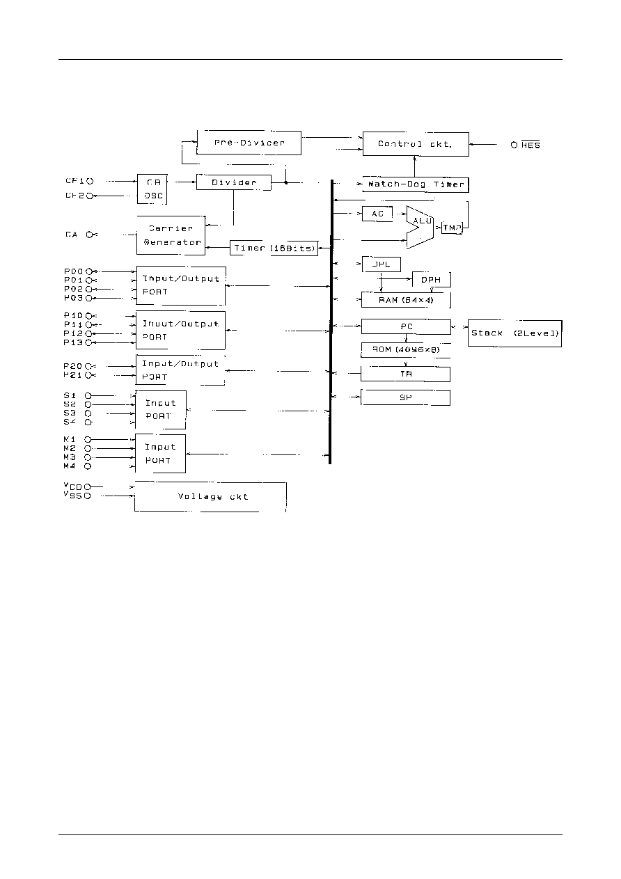
(A) Block Diagram
(LC573104A)
LC573104A, 573102A
No.4144≠5/16
Die Specifications
Chip size :
3.51mm
◊
3.19mm
Chip thickness :
480
µ
m
Pad size :
120
µ
m
◊
120
µ
m
Pad Layout
Pad coordinates
17
18
19
20
21
22
23
24
1
2
3
4
5
1465
1155
≠ 305
≠ 1485
≠ 1485
≠ 1485
≠ 1485
≠ 1485
≠ 1485
≠ 1485
≠ 1485
≠ 1485
≠ 410
1365
1365
1365
1365
1110
870
565
325
20
≠ 220
≠ 480
≠ 1395
≠ 1395
1
2
3
4
5
6
7
8
9
10
11
12
13
VDD
CA
P20
P21
P00
P01
P02
P03
P10
P11
P12
P13
S1
MFP24S pin assignment
X
(
µ
m)
Y
(
µ
m)
Pad
No.
Pin
Name
6
7
8
≠
≠
9
10
11
12
13
14
15
16
360
560
760
960
1140
1560
1560
1560
1560
1465
1465
1465
1465
≠ 1395
≠ 1395
≠ 1395
≠ 1395
≠ 1395
≠ 1395
≠ 905
≠ 685
≠ 445
330
570
755
1155
14
15
16
17
18
19
20
21
22
23
24
25
26
S2
S3
S4
TEST
TEST
M1
M2
M3
M4
RES
VSS
CF1
CF2
MFP24S pin assignment
X
(
µ
m)
Y
(
µ
m)
Pad
No.
Pin
Name
∑ The chip center is the origin of the above pad coordinates.
The X, Y values represent the coordinate of the pad center.
∑ When dipping the MFP24S package in solder to mount on boards, contact SANYO for instructions, etc.
∑ Chip substrate should be connected to V
SS
or left open.