 | –≠–ª–µ–∫—Ç—Ä–æ–Ω–Ω—ã–π –∫–æ–º–ø–æ–Ω–µ–Ω—Ç: LC5739 | –°–∫–∞—á–∞—Ç—å:  PDF PDF  ZIP ZIP |
91400 RM (IM) HO No.6704-1/18
Ver.1.14
22698
Preliminary
Overview
The LC5739 is a CMOS 4-bit microcontroller that operates on low voltage and very low power consumption. It also
contains 4K-byte ROM, 128-byte RAM, LCD drivers and melody function.
Features
(1) ROM
:4096
◊
8 bits
(2) RAM
:128
◊
4 bits
(3) Cycle Time
Cycle Time
Oscillation source
Oscillation frequency
Power supply voltage
Power source
Crystal oscillation
122
µ
s
RC oscillation
32.768kHz
1.30 - 1.65V
Ag Battery
122
µ
s
Crystal oscillation
32.768kHz
2.60 - 3.60V
Li Battery
Crystal oscillation
122
µ
s
RC oscillation
32.768kHz
2.60 - 3.60V
External voltage
supply
(4) Input / Output Terminals
- Input ports
: 4 terminals (S-port : 4 terminals)
- Input / Output ports
: 8 terminals (P0 port : 4 terminals, P1 port : 4 terminals)
- Output ports
: 2 terminals (Buzzer / melody output terminal : 1 terminal,
General output port : 1 terminal)
- LCD segment output ports
: 32 terminals (Possible to use output port by mask option)
- LCD common output ports
: 4 terminals
4-Bit Microcontroller
with LCD Driver
LC5739
Ordering number : ENN*6704
CMOS IC
LC5739
No.6704-2/18
(5) LCD driver
Drivable LCD panel
Number of drivable LCD segment output
1/2 bias 1/4 duty
128 segments
1/2 bias 1/3 duty
96 segments
1/2 bias 1/2 duty
64 segments
STATIC 32
segments
(Possible to use output port by mask option.)
- Built-in Step-up / Step-down circuit
(6) Melody/Buzzer
- Melody function
Octave
: 3 octaves
Time of musical note
: specified by program
- Buzzer output
(7) Base timer
- 15-bit base timer for timekeeping
(8) HALT release
- Five vectors
1. 15-bit base timer (500ms overflow output)
2. 15-bit base timer (output every 32ms)
3. S-port
4. P1-port
5. 1/10 second pulse
(9) Stand-by mode
- HALT mode
The program operation will be stopped in this mode. This mode is released by system reset and 5 vectors for HALT
release above-mentioned.
(10) System reset
- RES terminal
- Reset by setting S1 to S4 terminals to "H" level simultaneously.
(11) Oscillation
- 32.768kHz crystal oscillation
- RC oscillation
(12) Power supply
- Ag-battery
: VDD1-VSS=1.30V to 1.65V, Step-up voltage (VDD2-VSS=2.4V to 3.3V)
- Li-battery
: VDD2-VSS=2.60V to 3.60V, Step-down voltage (VDD1-VSS=1.3V to 1.8V)
- External voltage supply : VDD2-VSS=2.00V to 3.60V, Step-down voltage (VDD1-VSS=1.3V to 1.8V)
(13) Shipping form
- Bare chip, QFP64
(14) The development tool
- Evaluation chip
: LC5797
- Emulator
: EVA510 + TB5739 + DCB-1A
LC5739
No.6704-3/18
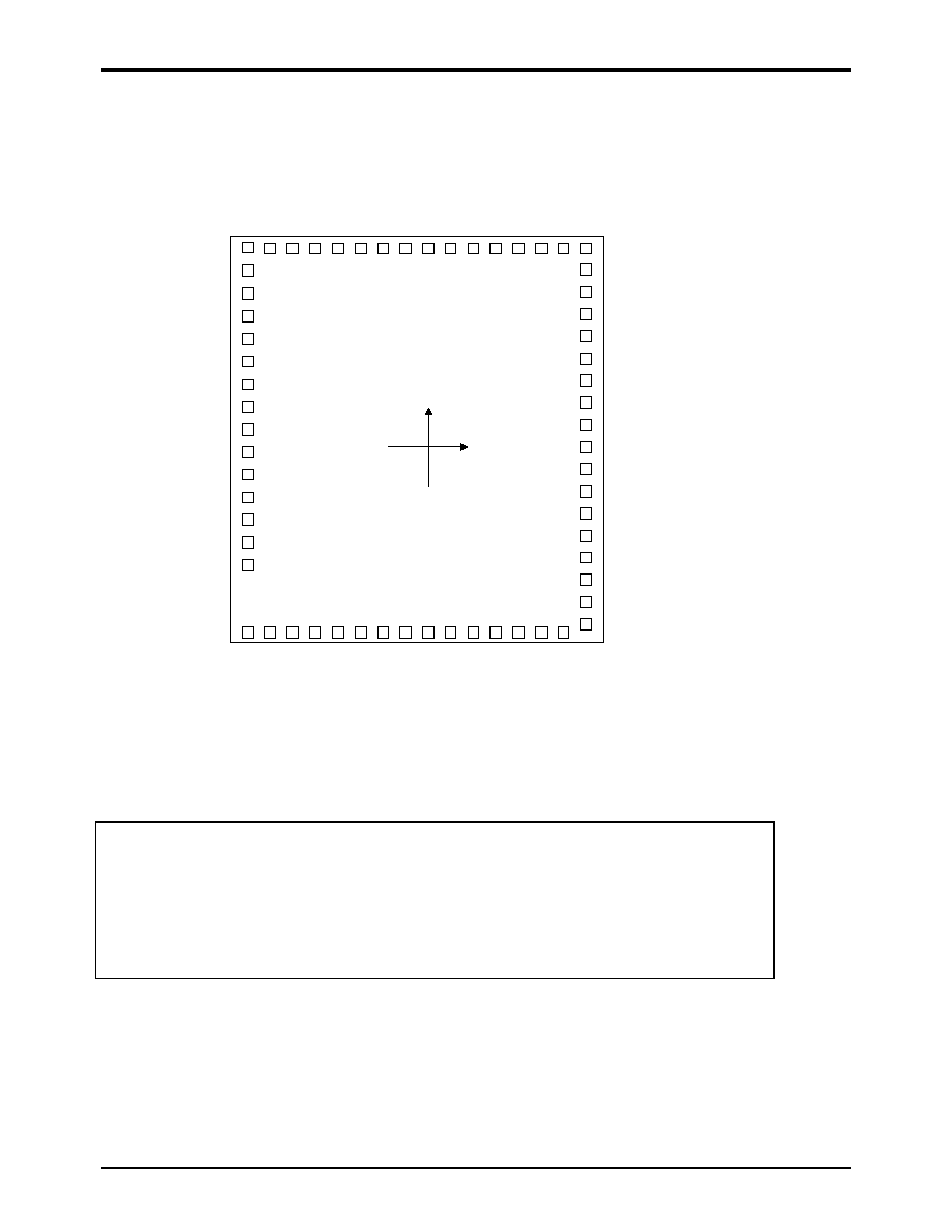
Pad assignment
Chip size (X
◊
Y)
: 2.63mm
◊
2.89mm
Chip thickness
: 480
µ
m
Pad size
: 116
µ
m
◊
116
µ
m
Note:
When a Lithium battery has been selected as the power supply, please note the following points.
There are two modes of use for the lithium battery: Backup mode and Normal mode (backup flag off). In backup
mode, the battery potential is applied directly to the oscillation circuit, whereas in Normal mode only half the
battery potential is applied.
Because of the different voltage applied to the oscillation circuit in each mode, there may be a difference in the
generated oscillation frequency. When entering backup mode a corresponding error will arise. If timing accuracy
is required (for clocks, etc), please bear in mind the above in the program design.
SEG3
SEG2
SEG1
COM2
TEST
OSCOUT
OSCIN
RES
S1
S2
32HZ
T3
CUP2
CUP1
COM1
SEG32
SEG31
ALM1
VDD2
VDD1
BAK
VSS
S4
S3
P10
P11
P12
P13
P00
P01
P02
P03
X
Y
LI
GH
T
CO
M3
SE
G
16
SE
G
15
SE
G
14
SE
G
13
SE
G
12
SE
G
11
SE
G
10
SE
G
9
SE
G
8
SE
G
7
SE
G
6
SE
G
5
SE
G
4
CO
M4
SE
G
1
7
SE
G
1
8
SE
G
1
9
SE
G
2
0
SE
G
2
1
SE
G
2
2
SE
G
2
3
SE
G
2
4
SE
G
2
5
SE
G
2
6
SE
G
2
7
SE
G
2
8
SE
G
2
9
SE
G
3
0
LC5739
No.6704-4/18
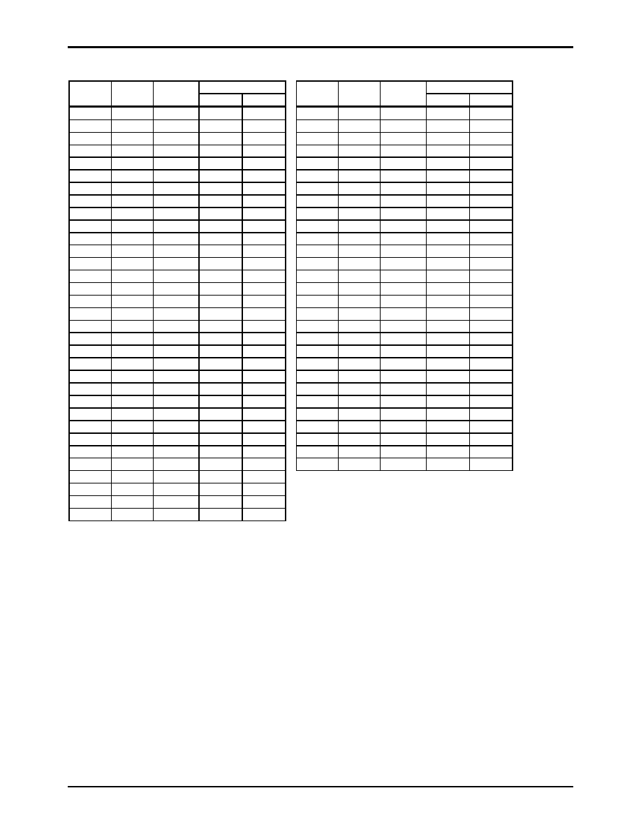
Pad name and coordinates
Coordinates Coordinates
QFP64
PIN No.
Pad
No.
Pad
Name
X
µ
m Y
µ
m
QFP64
PIN No.
Pad
No.
Pad
Name
X
µ
m Y
µ
m
3 1
BAK -1065 755 38 34
32HZ 1065
-405
4 2
VSS -1065 615 39 35
S2
1065
-265
5 3
S4 -1065 475 40 36
S1
1065
-125
6 4
S3 -1065 335 41 37
RES 1065 15
7 5
P10 -1065 175 42 38
OSCIN
1065
155
8 6
P11 -1065 15 43 39
OSCOUT
1065
295
9 7
P12 -1065
-145 44 40
TEST 1065
435
10 8
P13 -1065 -305 45 41
COM2 1065
575
11 9
P00 -1065 -470 46 42
SEG1 1065
715
12
10 P01
-1065
-630
47
43 SEG2
1065 855
13
11 P02
-1065
-790
48
44 SEG3
1065 995
14
12 P03
-1065
-950
49
45 SEG4
1105 1205
15
13 COM4 -1105 -1205
50
46 SEG5
965 1205
17
14 SEG17 -965 -1205
51
47 SEG6
825 1205
18
15 SEG18 -825 -1205
52
48 SEG7
685 1205
19
16 SEG19 -685 -1205
53
49 SEG8
545 1205
20
17 SEG20 -545 -1205
54
50 SEG9
405 1205
21
18 SEG21 -405 -1205
55
51 SEG10
265 1205
22
19 SEG22 -265 -1205
56
52 SEG11
125 1205
23
20 SEG23 -125 -1205
57
53 SEG12
-15 1205
24
21 SEG24
15 -1205
58
54 SEG13
-155 1205
25 22
SEG25 155
-1205 59 55
SEG14 -295
1205
26 23
SEG26 295
-1205 60 56
SEG15 -435
1205
27 24
SEG27 435
-1205 61 57
SEG16 -575
1205
28 25
SEG28 575
-1205 62 58
COM3 -715
1205
29 26
SEG29 715
-1205 63 59
LIGHT -855
1205
30 27
SEG30 855
-1205 64 60
ALM -1065
1245
31
28 SEG31 1065 -1245
1
61 VDD2 -1065 1035
33
29 SEG32 1065 -1105
2
62 VDD1 -1065 895
34 30
COM1 1065 -965
35 31
CUP1 1065 -825
36 32
CUP2 1065 -685
37 33
T3
1065 -545
∑ The pad coordinates are such that the chip center is taken as the origin and the values for (X, Y) represent the coordinates of
the center point of each pad.
∑ Substrate must be connected to VSS or left open.
LC5739
No.6704-5/18
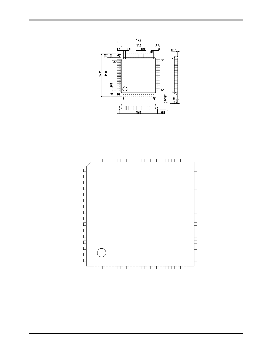
Package Dimension
(unit : mm)
3159
SANYO : QIP-64E
Pin Assignment
49
50
51
52
53
54
55
56
57
58
59
60
61
62
63
64
32
31
30
29
28
27
26
25
24
23
22
21
20
19
18
17
48
47
46
45
44
43
42
41
40
39
38
37
36
35
34
33
1
2
3
4
5
6
7
8
9
10
11
12
13
14
15
16
NC
SEG31
SEG30
SEG29
SEG28
SEG27
SEG26
SEG25
SEG24
SEG23
SEG22
SEG21
SEG20
SEG19
SEG18
SEG17
SEG4
SEG5
SEG6
SEG7
SEG8
SEG9
SEG10
SEG11
SEG12
SEG13
SEG14
SEG15
SEG16
SEG17
SEG18
SEG19
SEG3
SEG2
SEG1
CO
M2
TEST
OS
CO
UT
OS
CI
N
RE
S
S1
S2
32
H
Z
T3
CU
P
2
CU
P
1
CO
M1
SEG3
2
VD
D2
VD
D1
BA
K
VS
S
S4
S3
P10
P11
P12
P13
P00
P01
P02
P03
CO
M4
NC