 | –≠–ª–µ–∫—Ç—Ä–æ–Ω–Ω—ã–π –∫–æ–º–ø–æ–Ω–µ–Ω—Ç: LC5852N | –°–∫–∞—á–∞—Ç—å:  PDF PDF  ZIP ZIP |
Ordering number : EN 4365B
O3095HA (OT)/91994TH (OT) No. 4365-1/29
Overview
The LC5852N is a high-performance four-bit single-chip
built-in LCD driver microprocessor that provides a variety
of attractive features including low-voltage operation and
low power dissipation. The LC5852N was developed as an
upwardly compatible version of the LC5851N and
provides a ROM capacity increased from 1024 to 2048 15-
bit words and a RAM capacity increased from 64
◊
4 bits
to 128
◊
4 bits.
Applications
∑ System control and LCD display in cameras, radios and
similar products
∑ System control and LCD display in miniature electronic
test equipment and consumer health maintenance
products
∑ The LC5852N is optimal for end products with LCD
displays and, in particular, for battery operated products.
Features
The LC5852N is an upwardly compatible version of the
LC5851N and, as such, has the following features.
∑ Extremely broad allowable operating ranges
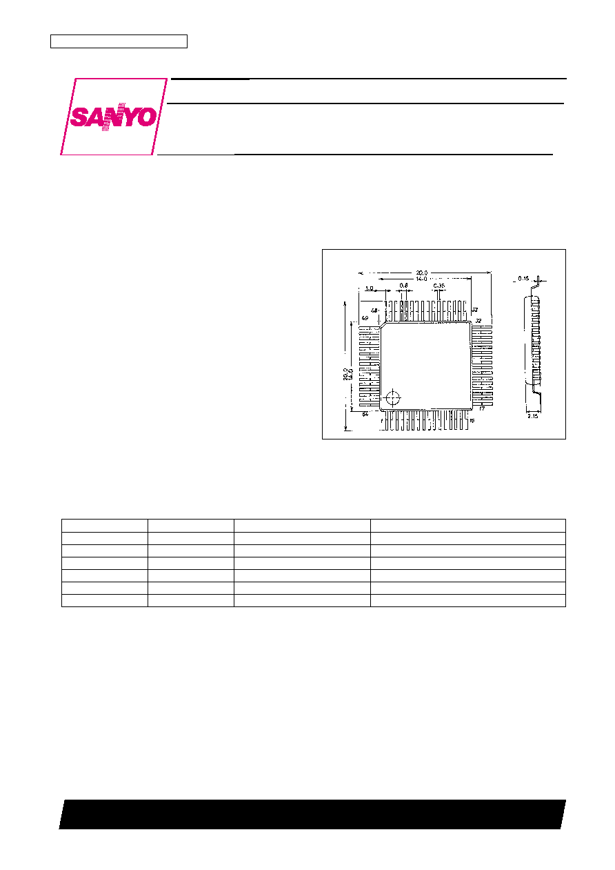
Package Dimensions
unit: mm
3057-QIP64A
SANYO: QIP64A
[LC5852N]
LC5852N
SANYO Electric Co.,Ltd. Semiconductor Bussiness Headquarters
TOKYO OFFICE Tokyo Bldg., 1-10, 1 Chome, Ueno, Taito-ku, TOKYO, 110-8534 JAPAN
Four-Bit Single-Chip Microcontroller with
On-Chip LCD Drivers for Small-Scale Control in
Medium-Speed Applications
CMOS LSI
Power supply option
Cycle time
Power supply voltage range
Note
EXT-V
10 µs
V
SS
2 = ≠4.0 to ≠5.5 V
When using an 800 kHz ceramic resonator
EXT-V
20 µs
V
SS
2 = ≠4.0 to ≠5.5 V
When using a 400 kHz ceramic resonator
EXT-V
61 µs
V
SS
2 = ≠2.3 to ≠5.5 V
When using a 65 kHz crystal oscillator
EXT-V
122 µs, 244 µs
V
SS
2 = ≠2.0 to ≠5.5 V
When using a 32 kHz crystal oscillator
Li
122 µs, 244 µs
V
SS
2 = ≠2.6 to ≠3.6 V
*
When using a 32 kHz crystal oscillator
Ag
122 µs, 244 µs
V
SS
1 = ≠1.3 to ≠1.65 V
When using a 32 kHz crystal oscillator
Note:
*
When the backup flag is set, the BAK pin is shorted to V
SS
2. (See the user's manual for details.)
∑ Low current drain
HALT mode (typical)
-- Ceramic oscillator (CF):
400 kHz (5.0 V)
150 µA
-- Crystal oscillator (Xtal):
32 kHz (1.5 V, Ag specifications)
2.0 µA (for LCD biases other than 1/3)
3.5 µA (for an LCD bias of 1/3)
-- Crystal oscillator (Xtal):
32 kHz (3.0 V, Li specifications)
1.0 µA (for LCD biases other than 1/3)
5.0 µA (for an LCD bias of 1/3)

∑ Timer functions
-- One six-bit programmable timer
-- Time base timer (for clock applications)
∑ Standby functions
-- Clock standby function (HALT mode)
The LC5852N provides a halt function that reduces
power dissipation. In halt mode, only the oscillator,
divider and LCD driver circuits operate. All other
internal operations are stopped. This mode allows
the LC5852N to easily implement a low-power
clock function.
-- Full standby function (HOLD mode)
-- HALT mode is cleared by two external factors and
two internal factors.
∑ Improved I/O functions
-- External interrupt pins
-- Input pins that can clear HALT mode (up to 9 pins)
-- Input ports with software controllable input resistors:
up to 8 pins
-- Input ports with built-in floating prevention circuits:
up to 8 pins
-- LCD drivers; common:
4 pins,
segment pins:
25 pins
-- General-purpose I/O ports:
8 pins
-- General-purpose inputs:
9 pins
-- General-purpose outputs (1):
6 pins
(ALM pin, LIGHT pin)
-- General-purpose outputs (2):
25 pins
(when all 25 LCD segment ports are used as general-
purpose outputs)
-- Pseudo-serial output port:
1 set
(Three pins: output, BUSY, clock)
Function Overview
∑ Program ROM: 2048
◊
15 bits
∑ On-chip RAM:
128
◊
4 bits
∑ All instructions execute in a single cycle
∑ HALT mode clear and interrupt functions
(External factors)
Changes in the S and M port input signals
Changes in the INT pin input signal
(Internal factors)
Overflow from the clock divider circuit
Timer underflow
∑ Subroutines can be nested up to four levels (including
interrupts)
∑ Powerful hardware to improve processing capabilities
-- On-chip segment PLA circuit and segment decoder:
The LCD driver outputs can handle LCD panel
segment display without incurring software
overhead.
-- All LCD driver output pins can be switched to be
used as output ports.
-- One six-bit programmable timer
-- Part of the RAM area can be used as a working area.
-- Built-in clock oscillator and 15-stage divider (also
used for LCD alternation signal generation)
∑ Highly flexible LCD panel drive output pins (25)
Supported
Maximum number Required
drive types
of segments
common pins
1/3 bias--1/4 duty......100 segments ..........4 pins
1/3 bias--1/3 duty......75 segments ............3 pins
1/2 bias--1/4 duty......100 segments ..........4 pins
1/2 bias--1/3 duty......75 segments ............3 pins
1/2 bias--1/2 duty......50 segments ............2 pins
Static ..........................25 segments ............1 pin
-- The LCD output pins can be converted to use as
general-purpose output pins.
CMOS type:
25 pins (maximum)
p-channel open drain type: 3 pins (maximum)
∑ An oscillator appropriate for the system specifications
can be selected.
32 or 65 kHz crystal oscillator, or
400 or 800 kHz ceramic oscillator
Delivery formats
QIP-64A or chip product
No. 4365-2/29
LC5852N
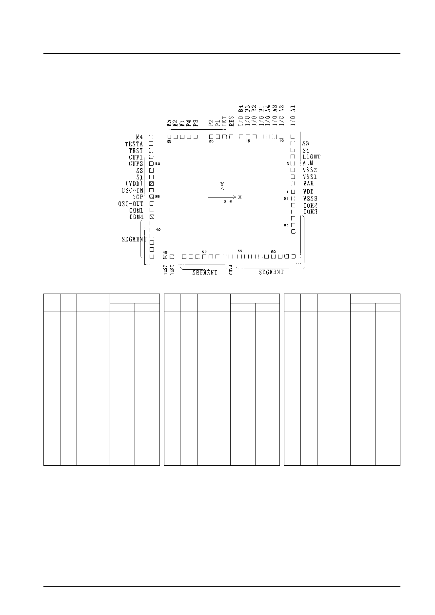
Pin and Pad Assignment
Chip size:
4.19
◊
3.66 mm
Pad size:
120
◊
120 µm
Chip thickness: 480 µm (chip specification products)
Note: 1. The pin numbers are those for the QIP-64A mass production package.
2. The pad coordinates given above take the center of the chip as the origin and specify the center of the pad.
3. TESTA pin (pin 2) in the QIP-64A product must be connected to the minus side of the power supply.
4. TEST pin (pin 3) in the QIP-64A product must be left open.
5. Pad 27 in the chip product must either be connected to the minus side of the power supply or left open.
6. Pads 28, 45 and 46 in the chip product must be left open.
7. If the chip product is used, the substrate must be connected to V
DD
.
8. Do not use dip-soldering techniques to mount the QIP-64A package product.
No. 4365-3/29
LC5852N
Pin
Pad
Symbol
Coordinates
No.
No.
Xµm
Yµm
40
1
V
DD
1899
138
41
2
BAK
1899
358
42
3
V
SS
1
1899
538
43
4
V
SS
2
1899
718
44
5
ALM
1899
898
45
6
LIGHT
1899
1078
46
7
S4
1899
1258
47
8
S3
1899
1438
48
9
I/O A1
1899
1630
49
10
I/O A2
1595
1630
50
11
I/O A3
1415
1630
51
12
I/O A4
1235
1630
52
13
I/O B1
1055
1630
53
14
I/O B2
875
1630
54
15
I/O B3
695
1630
55
16
I/O B4
515
1630
56
17
RES
253
1630
57
18
INT
73
1630
58
19
P1
≠107
1630
59
20
P2
≠287
1630
60
21
P3
≠707
1630
61
22
P4
≠887
1630
62
23
M1
≠1067
1630
Pin
Pad
Symbol
Coordinates
No.
No.
Xµm
Yµm
63
24
M2
≠1247
1630
64
25
M3
≠1427
1630
1
26
M4
≠1899
1630
2
27
TESTA
≠1899
1450
3
28
TEST
≠1899
1270
4
29
CUP1
≠1899
1090
5
30
CUP2
≠1899
910
6
31
S2
≠1899
730
7
32
S1
≠1899
550
--
33
(V
DD
)
≠1899
370
8
34
OSC-IN
≠1899
190
--
35
10P
≠1899
10
9
36
OSC-OUT
≠1899
≠169
10
37
COM1
≠1899
≠349
--
38
COM4
≠1899
≠529
11
39
Seg01
≠1899
≠709
12
40
Seg02
≠1899
≠889
13
41
Seg03
≠1899
≠1069
14
42
Seg04
≠1899
≠1249
15
43
Seg05
≠1899
≠1429
16
44
Seg06
≠1899
≠1609
--
45
TEST
≠1553
≠1630
--
46
TEST
≠1373
≠1630
Pin
Pad
Symbol
Coordinates
No.
No.
Xµm
Yµm
17
47
Seg07
≠1033
≠1630
18
48
Seg08
≠853
≠1630
19
49
Seg09
≠673
≠1630
20
50
Seg10
≠493
≠1630
21
51
Seg11
≠313
≠1630
22
52
Seg12
≠133
≠1630
23
53
Seg13
46
≠1630
24
54
COM4
226
≠1630
25
55
Seg14
459
≠1630
26
56
Seg15
639
≠1630
27
57
Seg16
819
≠1630
28
58
Seg17
999
≠1630
29
59
Seg18
1179
≠1630
30
60
Seg19
1359
≠1630
31
61
Seg20
1539
≠1630
32
62
Seg21
1719
≠1630
33
63
Seg22
1899
≠1630
34
64
Seg23
1899
≠954
35
65
Seg24
1899
≠774
36
66
Seg25
1899
≠594
37
67
COM3
1899
≠414
38
68
COM2
1899
≠234
39
69
V
SS
3
1899
≠54

System Block Diagram
LC5852N System Block Diagram
No. 4365-4/29
LC5852N
AC:
Accumulator
ALU:
Arithmetic and logic unit
INT CTL: Interrupt control circuit
PC:
Program counter
TM:
Preset timer (6 bits)
IR:
Instruction register
HALT:
Intermittent control circuit
SCG:
System clock generator
STS1:
Status register 1
STS2:
Status register 2
STS3:
Status register 3
CF:
Carry flag
BCF:
Backup flag
SCF1:
M port flag
SCF2:
STS3 flag
SCF3:
S port flag
SCF4:
INT signal change flag
SCF5:
Timer overflow flag
¯15:
Contents of the fifteenth stage of the divider
circuit
SCF7:
Divider circuit overflow flag
Pin Functions
No. 4365-5/29
LC5852N
Pin
I/O
QIP-64
Function
Option
At reset
Pin No.
V
DD
BAK
V
SS
1
V
SS
2
V
SS
3
CUP1
CUP2
OSC-IN
OSC-OUT
10P
S1
S2
S3
S4
M1
M2
M3
M4
I/O A1
I/O A2
I/O A3
I/O A4
I/O B1
I/O B2
I/O B3
I/O B4
P1
P2
P3
P4
ALM
LIGHT
--
--
--
--
--
--
--
Input
Output
--
Input
Input
I/O
I/O
Output
Output
Output
40
41
42
43
39
4
5
8
9
--
7
6
47
46
62
63
64
1
48
49
50
51
52
53
54
55
58
59
60
61
44
45
Power supply plus side
LSI internal logic block minus power supply
In Li specification products, connect a capacitor between BAK and V
DD
to prevent incorrect operation.
Power supply minus side
∑ External component connections differ depending on mask options
and other factors.
In products for Ag use, connect V
SS
1 to the power supply minus side.
In other products, connect V
SS
2 to the power supply minus side.
∑ The pins other than the minus pin are used for the LCD driver power
supply.
Connections for the LCD drive voltage boost (cut) capacitor.
Used for real-time clock and the system clock.
Connected to OSC-IN or OSC-OUT and used for the oscillator phase
compensation capacitor. Can only be used in the chip product.
Dedicated input port
∑ Includes either a ¯10 (32 ms), ¯8 (8 ms), or ¯2 (2 ms) chattering
exclusion circuit (PLA mask option).
*
These values are for the case where a 32.768 kHz crystal is used.
∑ Pull-down resistors are built in.
Dedicated input port
∑ Input connections for acquiring data to internal RAM
∑ Pull-down resistors are built in.
I/O port
∑ Input connections for acquiring data to internal RAM
∑ Output connections for data output from internal RAM
∑ The input or output state can be switched by two instructions.
I/O port
∑ Input connections for acquiring data to internal RAM
∑ Output connections for data output from internal RAM
∑ The input or output state can be switched by two instructions.
Output port
∑ Output connections for data output from internal RAM
Dedicated output
This pin can output a signal modulated either at 4 kHz or 2 kHz, or at
4 kHz or 1 kHz under program control. Alternatively, an unmodulated
signal can be output.
*
These values are for the case where a 32.768 kHz crystal is used.
Dedicated output
This pin can drive a power transistor.
∑ Ag specifications
∑ Li specifications
∑ EXT-V
specifications
∑ Crystal oscillator
use (XT option)
∑ Ceramic resonator
use (CF option)
The CF option can
only be specified for
EXT-V specification
products.
Inclusion
(or exclusion) of a
low level hold
transistor
Inclusion
(or exclusion) of a
low level hold
transistor
∑ Modulated signals
(4 kHz, 2 kHz, or
unmodulated)
∑ Modulated signals
(4 kHz, 1 kHz, or
unmodulated)
Backup flag set
Backup flag cleared
(depending on the
power supply option)
The pull-down
resistor transistor is
on.
The pull-down
resistor transistor is
on.
Input mode
Input mode
Either a high- or
low-level output.
(Undefined)
Low-level output
Low-level output
Continued on next page.