N3000 RM (IM) TY No.6829-1/22
Ver.1.01
62600
Preliminary
Overview
The LC65F1306A belongs to our 4-bit single-chip microcontroller LC6500 series fabricated using CMOS process
technology. They are ideally suited for use in small-scale control applications. Their basic architecture and instruction set
are the same. These microcontrollers include an 8-input 8-bit A/D converter and are appropriate for use in a wide range of
applications. That range includes applications with a small number of control circuits that were previously implemented in
standard logic, and applications with a larger scale such as home appliances, automotive equipment, communications
equipment, office equipment, and audio equipment such as decks and players. This microcontroller, with some exceptions,
has identical functions to the LC651306A, 1304A, 1302A and 1301A mask ROM version microcontrollers. It can also be
used as an OTP version microcontroller. Further, through a rewrite operation on the FLASH memory, the LC65F1306A can
be used in applications where previously microcontrollers of this type could not have been implemented.
Features
1) CMOS technology for a low-power consumption operation (A standby function that can be invoked under program
control is also provided.)
2) Flash ROM/RAM
LC65F1306A Flash ROM : 6K
◊
8 bits, RAM : 256
◊
4 bits
3) Instruction set : 81 instructions common to all microcontrollers of the LC6500 series
4) Wide operating voltage range : 3.0 V to 5.5 V
5) Instruction cycle time : 0.92
µ
s
6) On-chip serial I/O port
4-Bit Single-Chip CMOS Microcontroller for
Small-Scale Control Applications
LC65F1306A
Ordering number : ENN*6829
CMOS IC

LC65F1306A
No.6829-2/22
7) Flexible I/O port
∑ Number of ports : 5 ports / 18 pins (max.)
∑ All ports
: Input / output common
Input / output capacity voltage 15V max. (open-drain specification C and D only)
Output current
20 mA max. sink current (Can drive an LED directly)
∑ Support option for system specification
Output level in the reset mode
: high/low level for port C and D specified in 4-bit unit
8) Interrupt function
Interrupt by timer overflow (can be tested under program control)
Interrupt by the state of the INT pin or completion of transmission/reception at serial I/O port (can be tested under
program control)
9) Stack level : 8 levels (common use with interrupt)
10) Timer :
4-bit variable prescaler + 8-bit programmable counter
11) Clock oscillation options for user's intended system
∑ Oscillator circuit options : two-pin RC oscillator
two-pin ceramic oscillator
∑ Divider circuit options : No divider
built-in divide by 3
built-in divide by 4
12) Continuous square wave output (64 times of the cycle time)
13) AD converter (successive approximation)
∑ Precise conversion (expressed in 8 bits), 8 input channels
14) Watchdog timer
∑ RC circuit time constant
∑ Watchdog timer reset function can be assigned to an external pin by the option.
15) Low voltage detection circuit
∑ Can be implemented by the option.
16) Factory shipment
∑ DIP24S, MFP24S
17) Flash Memory
∑ Rewrite block size :
128 bytes / page
∑ Erase / write voltage :
3.0 to 5.5V
∑ Rewritable limit :
10000 times (target number, to be decided after evaluation)
∑ Operating temperature : 0 to +85
∞
C (when writing to the flash memory)
-20 to +85
∞
C (when reading from the flash memory)

LC65F1306A
No.6829-3/22
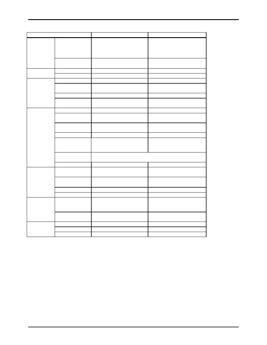
Function Table
Parameter LC651306A/04A/02A/01A
LC65F1306A
ROM
6144
◊
8 bits (1306A)
4096
◊
8 bits (1304A)
2048
◊
8 bits (1302A)
1024
◊
8 bits (1301A)
6144
◊
8 bits
Memory
RAM
256
◊
4 bits
(1306A/04A/02A/01A)
256
◊
4 bits
Instruction set
81
81
Instructions
Table reference
Supported
Supported
Interrupt
1 external, 1 internal
1 external, 1 internal
Timer
4-bit variable prescaler + 8-bit
timers
4-bit variable prescaler + 8-bit
timers
Stack level
8
8
On-chip
functions
Standby function
Standby mode by the HALT
instruction supported
Standby mode by the HALT
instruction supported
Port number
18 I/O port pins
22 I/O port pins
Serial port
Input and output in 4 or 8 bit
units
Input and output in 4 or 8 bit
units
I/O voltage
capacity
15 V max.
15 V max.
Output current
10 mA typ. 20 mA max.
10 mA typ. 20 mA max.
I/O
circuit
type
Open drain (N-channel) or
pull-up resistor output option
can be specified in 1- bit unit.
Open drain (N-channel)
Output level at
reset
High or low level output can be selected in port unit (ports C and D
only)
I/O ports
Square wave output
Supported
Supported
Minimum cycle
time
0.92
µ
s (VDD
2.5 V)
0.92
µ
s (VDD
3.0 V)
Operating
temperature
-40
∞
C to +85
∞
C 0
∞
C to +85
∞
C (when writing)
-20
∞
C to +85
∞
C (when reading)
Supply voltage
2.5 to 6 V
3.0 to 5.5 V
Characteristics
Supply current
1.5 mA typ.
3 mA typ.
Oscillator
RC (800 kHz typ.)
Ceramic (400k, 800k,1MHz,
4MHz)
RC (800 kHz typ.)
Ceramic (400k, 800k,1MHz,
4MHz)
Oscillator
Divider circuit
option
1/1, 1/3, 1/4
1/1, 1/3, 1/4
Package
DIP24S MFP24S SSOP24
DIP24S MFP24S
Watchdog timer
Supported
Supported
Other items
OTP
Only DIP24S MFP24S
-
Note: The above oscillator and oscillator circuit constants are tentative. They will be announced as the recommended circuits
for these microcontrollers are determined. Please confirm the progress of these developments periodically.

LC65F1306A
No.6829-4/22
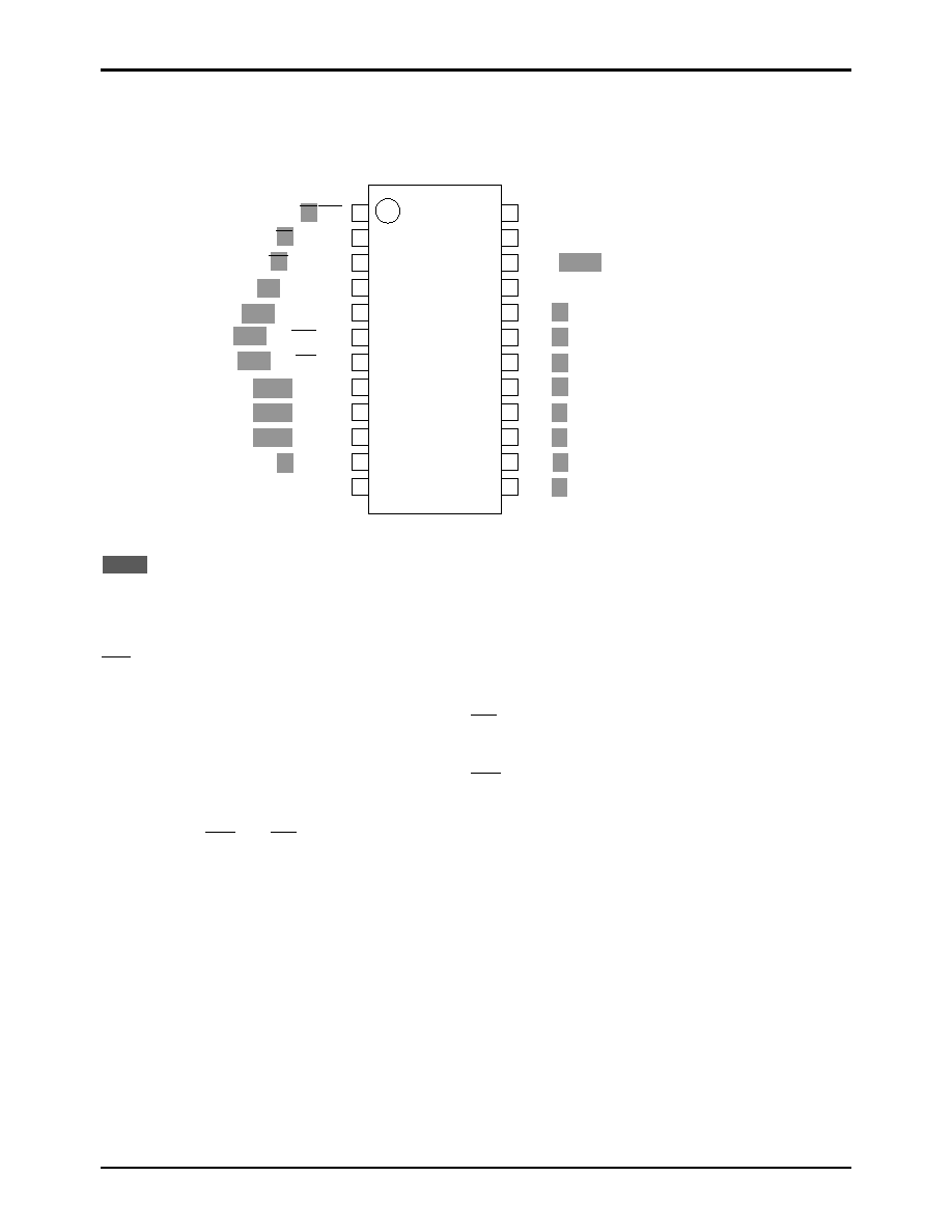
Pin Assignment
DIP24S, MFP24S
: Pin function names used when writing data to on-chip Flash ROM with the PROM writer
Pin Functions
OSC1, OSC2 :
Ceramic Oscillator for OSC, RC
TEST
:
Test
RES
:
Reset
AD0-AD7 :
AD converter analog input
PA0-3
:
Common I/O port A0-3
SQR
:
Square wave output
PC0-3
:
Common I/O port C0-3
WDR
:
Watch Dog Reset pin
PD0-3
:
Common I/O port D0-3
INT :
Interrupt
Request
pin
PE0-1
:
Common I/O port E0-1
SI
:
Serial Input pin
PF0-3
:
Common I/O port F0-3
SO
:
Serial Output pin
SCK
:
Serial Clock input/output pin
Notes:
∑
SQR and WDR are common with PE0 and PE1 respectively.
∑
SI, SO, SCK, and INT are common with PF0 to PF3 respectively.
1
2
3
4
5
6
7
8
9
10
11
12
24
23
22
21
20
19
18
17
16
15
14
13
OSC1
OSC2
TEST/EPMOD
VSS
PD3/D7
PD2/D6
PD1/D5
PD0/D4
PC3/D3
PC2/D2
PC1/D1
PC0/D0
CE/RES
OE/PE0/SQR
WE/PE1/WDR
ALE/PF0/SI/AD4
A0/A7/PF1/SO/AD5
A1/A8/PF2/SCK/AD6
A2/A9/PF3/INT/AD7
A3/A10/PA0/AD0
A4/A11/PA1/AD1
A5/A12/PA2/AD2
A6/PA3/AD3
VDD

LC65F1306A
No.6829-5/22
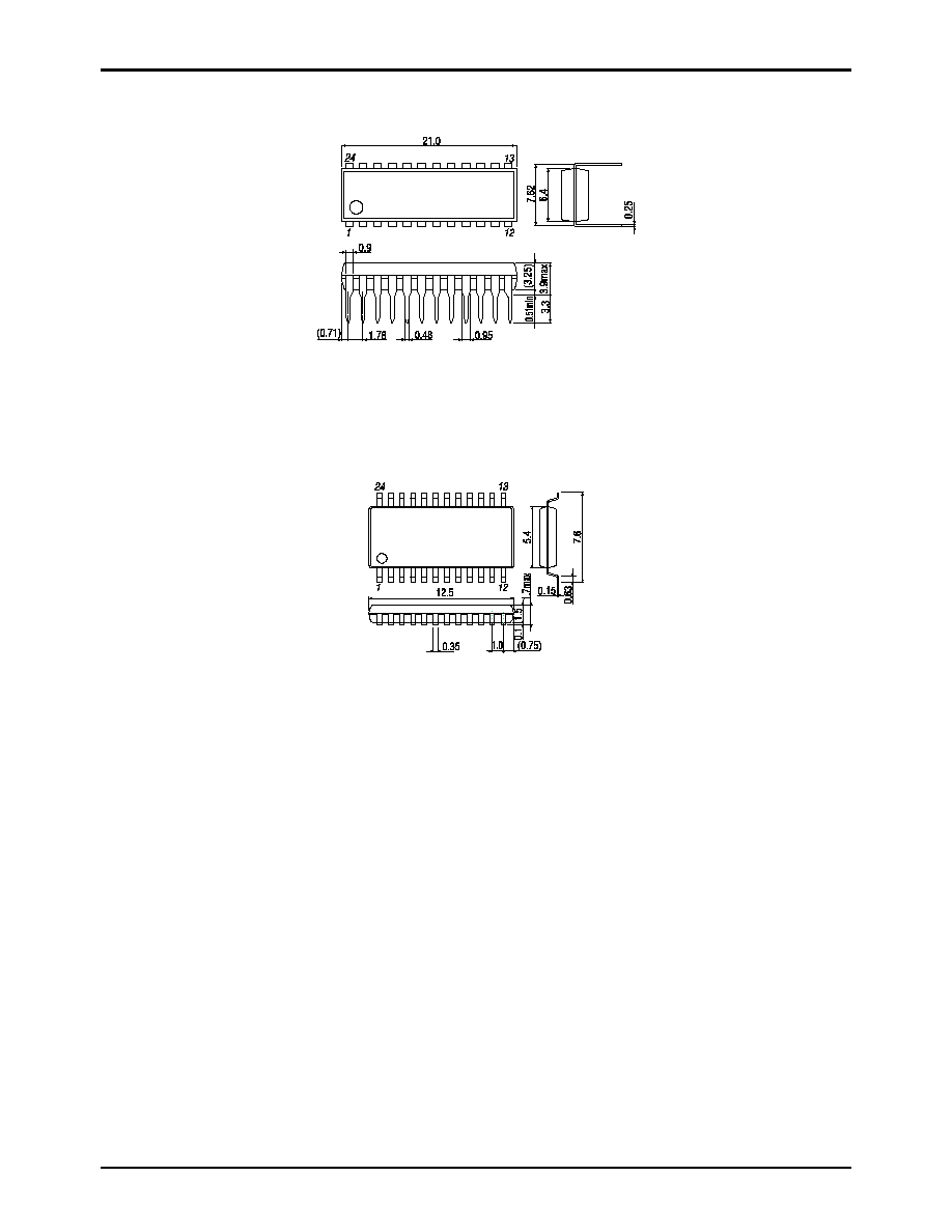
Package Dimension
(unit : mm)
3067A
SANYO : DIP24S(300mil)
Package Dimension
(unit : mm)
3112A
SANYO : MFP24S(300mil)


