 | –≠–ª–µ–∫—Ç—Ä–æ–Ω–Ω—ã–π –∫–æ–º–ø–æ–Ω–µ–Ω—Ç: LC66P2316 | –°–∫–∞—á–∞—Ç—å:  PDF PDF  ZIP ZIP |

22897HA (OT) No. 5489-1/28
Overview
The LC66P5316 is an on-chip OTP PROM version of the
LC6653XX Series CMOS 4-bit single-chip micro-
controllers. The LC66P5316 is appropriate for program
development and product evaluation since it provides
identical functionality and pin compatibility with the
LC665316A.
Features and Functions
∑ On-chip OTP ROM capacity of 16 kilobytes, and an on-
chip RAM capacity of 512
◊
4 bits.
∑ Fully supports the LC66000 Series common instruction
set (128 instructions).
∑ I/O ports: 42 pins
∑ A sub-oscillator circuit can be used (option)
This circuit allows power dissipation to be reduced by
operating at lower speeds.
∑ 8-bit serial interface: two circuits (can be connected in
cascade to form a 16-bit interface)
∑ Instruction cycle time: 0.95 to 10 µs (at 4.0 to 5.5 V)
∑ Powerful timer functions and prescalers
-- Time limit timer, event counter, pulse width
measurement, and square wave output using a 12-bit
timer.
-- Time limit timer, event counter, PWM output, and
square wave output using an 8-bit timer.
-- Time base function using a 12-bit prescaler
∑ Powerful interrupt system with 8 interrupt factors and 8
interrupt vector locations.
-- External interrupts: 3 factors/3 vector locations
-- Internal interrupts: 5 factors/5 vector locations
∑ Flexible I/O functions
16-value comparator inputs, 20-mA drive outputs,
inverter circuits, pull-up and open-drain circuits
selectable as options.
∑ Optional runaway detection function (watchdog timer)
∑ 8-bit I/O functions
∑ Power saving functions using halt and hold modes.
∑ Packages: DIP48S, QIP48E (QFP48E)
∑ Evaluation LSIs: LC66599 (evaluation chip) +
EVA800/850-TB662YXX2
Package Dimensions
unit: mm
3149-DIP48S
unit: mm
3156-QFP48E
Preriminary
LC66P5316
SANYO Electric Co.,Ltd. Semiconductor Bussiness Headquarters
TOKYO OFFICE Tokyo Bldg., 1-10, 1 Chome, Ueno, Taito-ku, TOKYO, 110 JAPAN
Four-Bit Single-Chip Microcontroller
with 16 KB of On-Chip OTP PROM
CMOS LSI
SANYO DIP48
0.48
1.05
1.78
2.53
46.0
15.24
0.51min
3.8
5.1max
4.25
13.8
0.25
24
1
25
48
SANYO: DIP48S
[LC66P5316]
(STAND OFF)
1.5
17.2
17.2
1.5
1.5
1.5
1.6
1.6
14.0
0.35
15.6
0.8
1.0
1.0
3.0max
2.70
0.1
0.15
1
12
24
25
13
48
36
14.0
37
SANYO: QFP48E
[LC66P5316]
No. 5489

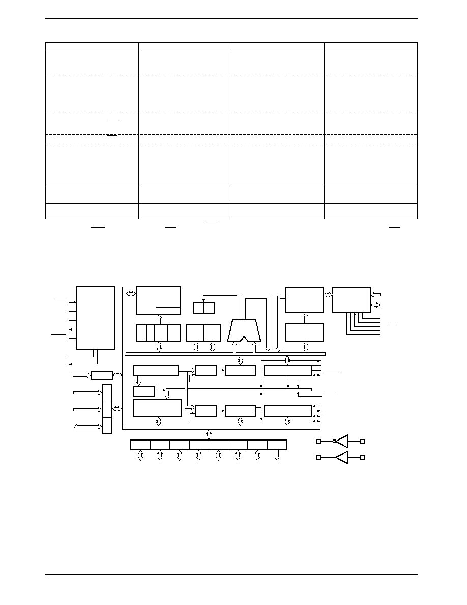
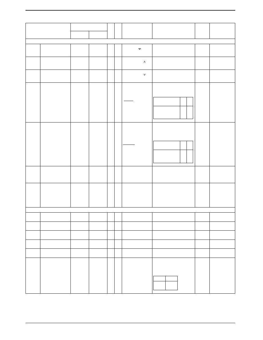
Series Organization
Note:
*
Under development
No. 5489-2/28
LC66P5316
Type No.
No. of
ROM capacity
RAM
Package
Features
pins
capacity
LC66304A/306A/308A
42
4 K/6 K/8 KB
512 W
DIP42S
QFP48E
LC66404A/406A/408A
42
4 K/6 K/8 KB
512 W
DIP42S
QFP48E
LC66506B/508B/512B/516B
64
6 K/8 K/12 K/16 KB
512 W
DIP64S
QFP64A
LC66354A/356A/358A
42
4 K/6 K/8 KB
512 W
DIP42S
QFP48E
LC66354S/356S/358S
42
4 K/6 K/8 KB
512 W
QFP44M
LC66556A/558A/562A/566A
64
6 K/8 K/12 K/16 KB
512 W
DIP64S
QFP64E
LC66354B/356B/358B
42
4 K/6 K/8 KB
512 W
DIP42S
QFP48E
Low-voltage high-speed versions
LC66556B/558B/562B/566B
64
6 K/8 K/12 K/16 KB
512 W
DIP64S
QFP64E
3.0 to 5.5 V/0.92 µs
LC66354C/356C/358C
42
4 K/6 K/8 KB
512 W
DIP42S
QFP48E
2.5 to 5.5 V/0.92 µs
LC662104A/06A/08A
30
4 K/6 K/8 KB
384 W
DIP30SD
MFP30S
LC662304A/06A/08A/12A/16A
42
4 K/6 K/8 K/12 K/16 KB 512 W
DIP42S
QFP48E
LC662508A/12A/16A
64
8 K/12 K/16 KB
512 W
DIP64S
QFP64E
LC665304A/06A/08A/12A/16A
48
4 K/6 K/8 K/12 K/16 KB 512 W
DIP48S
QFP48E
Dual oscillator support
3.0 to 5.5 V/0.95 µs
LC66E308
42
EPROM 8 KB
512 W
DIC42S
QFC48
with window
with window
LC66P308
42
OTPROM 8 KB
512 W
DIP42S
QFP48E
LC66E408
42
EPROM 8 KB
512 W
DIC42S
QFC48
with window
with window
LC66P408
42
OTPROM 8 KB
512 W
DIP42S
QFP48E
LC66E516
64
EPROM 16 KB
512 W
DIC64S
QFC64
with window
with window
LC66P516
64
OTPROM 16 KB
512 W
DIP64S
QFP64E
LC66E2108
*
30
EPROM 8 KB
384 W
LC66E2316
42
EPROM 16 KB
512 W
DIC42S
QFC48
with window
with window
LC66E2516
64
EPROM 16 KB
512 W
DIC64S
QFC64
with window
with window
LC66E5316
52/48
EPROM 16 KB
512 W
DIC52S
QFC48
with window
with window
LC66P2108
*
30
OTPROM 8 KB
384 W
DIP30SD
MFP30S
LC66P2316
*
42
OTPROM 16 KB
512 W
DIP42S
QFP48E
LC66P2516
64
OTPROM 16 KB
512 W
DIP64S
QFP64E
LC66P5316
48
OTPROM 16 KB
512 W
DIP48S
QFP48E
OTP
4.0 to 5.5 V/0.95 µs
Window evaluation versions
4.5 to 5.5 V/0.92 µs
Window and OTP evaluation versions
4.5 to 5.5 V/0.92 µs
On-chip DTMF generator versions
3.0 to 5.5 V/0.95 µs
Low-voltage versions
2.2 to 5.5 V/3.92 µs
Normal versions
4.0 to 6.0 V/0.92 µs

Pin Assignments
We recommend the use of reflow soldering techniques to solder-mount QFP packages.
Please consult with your Sanyo representative for details on process conditions if the package itself is to be directly
immersed in a dip-soldering bath (dip-soldering techniques).
No. 5489-3/28
LC66P5316
1
2
3
4
5
6
7
8
9
10
11
12
13
14
15
16
17
18
19
20
21
22
23
24
48
47
46
45
44
43
42
41
40
39
38
37
36
35
34
33
32
31
30
29
28
27
26
25
DIP48S
P20/SI0/A0
P21/SO0/A1
P22/SCK0/A2
P23/INT0/A3
P30/INT1/A4
P31/POUT0/A5
P32/POUT1/A6
VSS
OSC1
OSC2
VDD
RES/VPP/OE
PE0/XT1
PE1/XT2
TEST/EPMOD
P33/HOLD
P40/INV0I/A7
P41/INV0O/A8
P42/INV1I/A9
P43/INV1O/A10
P50/A11
P51/A12
P52/A13
P53/INT2/TA
P13/D7
P12/D6
P11/D5
P10/D4
P03/D3
P02/D2
P01/D1
P00/D0
PD3/AN4/INV4O
LC66P5316
PD2/AN3/INV4I
PD1/AN2/INV3O
PD0/AN1/INV3I
PC3/INV2O/DASEC
PC2/INV2I/CE
PC1
PC0
P83
P82
P81/DS1
P80/DS0
P63/PIN1
P62/SCK1
P61/SO1
P60/SI1
QFP48E
LC66P5316
36
37
P02/D2
P01/D1
1
P32/POUT1/A6
35
P00/D0
2
V
SS
34
PD3/AN4/INV4O
3
OSC1
33
PD2/AN3/INV4I
4
OSC2
32
PD1/AN2/INV3O
5
V
DD
31
PD0/AN1/INV3I
6
RES/V
PP
/OE
30
PC3/INV2O/DASEC
7
PE0/XT1
29
PC2/INV2I/
CE
8
PE1/XT2
28
PC1
9
TEST/EPMOD
27
PC0
10
P33/HOLD
26
P83
11
P40/INV0I/A7
25
P82
12
P41/INV0O/A8
24
P81/DS1
38
P03/D3
23
P80/DS0
39
P10/D4
22
P63/PIN1
40
P11/D5
21
P62/SCK1
41
P12/D6
20
P61/SO1
42
P13/D7
19
P60/SI1
43
P20/SI0/A0
18
P53/INT2/TA
44
P21/SO0/A1
17
P52/A13
45
P22/SCK0/A2
16
P51/A12
46
P23/INT0/A3
15
P50/A11
47
P30/
INT1
/A4
14
P43/INV1O/A10
48
P31/POUT0/A5
13
P42/INV1I/A9
Top view
Usage Notes
The LC66P5316 was created for program development, product evaluation, and prototype development for products
based on the LC6653XX Series microcontrollers. Keep the following points in mind when using this product.
1. After a reset
The RES pin must be held low for an additional 3 instruction cycles after the oscillator stabilization period has
elapsed. Also, the port output circuit types are set up during the 9 instruction cycles immediately after RES is set
high. Only then is the program counter set to 0 and program execution started from that location. (The port output
circuits all revert to the open-drain type during periods when RES is low.)
2. Notes on LC6653XX evaluation
The high end of the EPROM area (locations 3FF0H to 3FFFH) are the option specification area. Option specification
data must be programmed for and loaded into this area. The Sanyo specified cross assembler for this product is the
program LC66S.EXE. Also, insert JMP instructions so that user programs do not attempt to execute addresses that
exceed the capacity of the mask ROM, and write zeros (00H) to areas (other than 3FF0H to 3FFFH) that exceed the
actual capacity of the mask ROM.
3. Mounting notes
Due to structural considerations, Sanyo is unable to fully test one-time programmable products. Therefore, the user
must apply the screening procedure described on page 20 to these products.
4. Use the following procedure when ordering ROM through the Sanyo PROM writing service. (Note that this is a for-
fee service.)
∑ If ordering one-time programmable and mask ROM versions at the same time:
The customer must provide the EPROM for the mask ROM version, the order forms for the mask ROM version,
and the order forms for the one-time programmable version.
∑ If ordering only the one-time programmable version:
The customer must provide the EPROM and the order forms for the one-time programmable version. The last
section of the EPROM (locations 3FF0H to 3FFFH) is the option specification area, and the option specification
data must be written to this area. The Sanyo specified cross assembler for this product is the program LC66S.EXE.
Also, insert JMP instructions so that user programs do not attempt to execute addresses that exceed the capacity of
the mask ROM, and write zeros (00H) to areas (other than 3FF0H to 3FFFH) that exceed the actual capacity of the
mask ROM.
5. Differences between this product and the mask ROM version:
Carefully read the sections on the following pages that describe these differences.
No. 5489-4/28
LC66P5316
At least 10 ms
VDD
min
Location
0
Location
1
VDD
OSC
RES
Program execution (PC)
Port output type
At least 3
instruction
Oscillator
stabilization
Open drain
Option switching
period
9 instruction
cycles
Option specification
Main differences between the LC66E5316, LC66P5316, and LC6653XX Series
Note:
*
Although the microcontroller will remain in hold mode if the RES pin is set low while it is in hold mode, always use the reset start sequence (after
switching HOLD from low to high, switch RES from low to high) when clearing hold mode. Also a current of about 100 µA flows from the RES pin
when it is low. This increases the hold mode current drain by about 100 µA.
See the data sheets for the individual products for details on other differences.
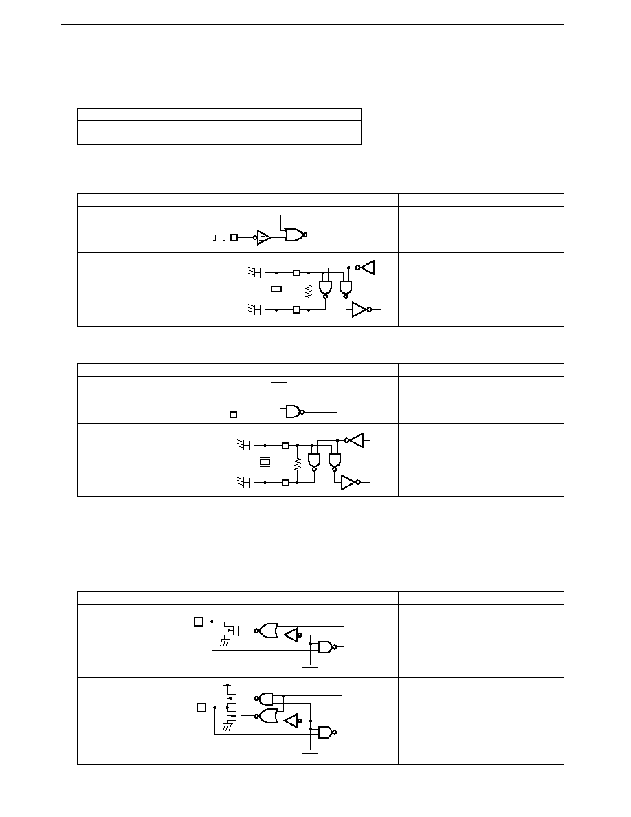
System Block Diagram
No. 5489-5/28
LC66P5316
Item
LC6653XX Series (mask version)
LC66E5316
LC66P5316
Differences in the main
characteristics
≠30 to +70∞C
+10 to +40∞C
≠30 to +70∞C
∑ Operating temperature range
3.0 to 5.5 V/0.95 to 10 µs
4.5 to 5.5 V/0.95 to 10 µs
4.0 to 5.5 V/0.92 to 10 µs
∑ Operating supply voltage/operating
(When the main oscillator is
(When the main oscillator is
(When the main oscillator is
frequency (cycle time)
operating)
operating)
operating)
3.0 to 5.5 V/25 to 127 µs
4.5 to 5.5 V/25 to 127 µs
4.0 to 5.5 V/25 to 127 µs
(When the sub-oscillator is operating) (When the sub-oscillator is operating)
(When the sub-oscillator is operating)
Typical: 10 µA
Typical: 10 µA
∑ Input high-level current (RES)
Maximum: 1 µA
(normal operation and halt mode)
(normal operation and halt mode)
Hold mode: 1 µA maximum
Hold mode: 1 µA maximum
∑ Input low-level current (RES)
Maximum: 1 µA
Typical: 100 µA
Typical: 100 µA
∑ Current drain
(Operating at 4 MHz)
(Operating at 32 kHz)
Typical: 10 nA, maximum: 10 µA
Larger than that for the mask versions
Larger than that for the mask versions
(Halt mode at 4 MHz)
Typical: 10 nA, maximum: 10 µA
*
Typical: 10 nA, maximum: 10 µA
*
(Halt mode at 32 kHz)
(Hold mode)
Port output types at reset
The output type specified in
Open-drain outputs
Open-drain outputs
the options
Package
∑ DIP48S
∑ DIC52S window package
∑ DIP48S
∑ QFP48E
∑ QFC48 window package
∑ QFP48E
SYSTEM
CONTROL
RAM STACK
(512W)
SP
E
A
OTP ROM
(16KB)
PROM
control
PC
POUT0
A0 to A13
D0 to D7
SI0
SO0
SCK0
INT0
CE
DASEC
VPP/OE
EPMOD
TA
INT1, INT2
PIN1, POUT1
INV
x
O
INV
x
I
(x=0 to 4)
FLAG
INTERRUPT
CONTROL
MPX
MPX
TIMER1
MPX
TIMER0
SERIAL I/O 0
PE
PD
PC
E
M
R
D
P
Y
D
P
X
D
P
L
D
P
H
P0
P1
P2
P3
P4
P5
P6
DS1
DS0
P8
C
Z
ALU
RES
XT1
XT2
AN1 to 4
TEST
OSC1
OSC2
HOLD
ADC
SI1
SO1
SCK1
SERIAL I/O 1
PRESCALER

Pin Function Overview
No. 5489-6/28
LC66P5316
Pin
I/O
Overview
Output driver type
Options
State after a Standby mode
reset
operation
P00/D0
P01/D1
P02/D2
P03/D3
P10/D4
P11/D5
P12/D6
P13/D7
P20/SI0/A0
P21/SO0/A1
P22/SCK0/
A2
P23/INT0/A3
P30/INT1/A4
P31/POUT0/
A5
P32/POUT1/
A6
P33/HOLD
P40/INV0I/
A7
P41/INV0O/
A8
P42/INV1I/
A9
P43/INV1O/
A10
I/O ports P00 to P03
∑ Input or output in 4-bit or 1-bit units
∑ P00 to P03 support the halt mode
control function (This function can be
specified in bit units.)
∑ Used as data pins in EPROM mode
I/O ports P10 to P13
∑ Input or output in 4-bit or 1-bit units
∑ Used as data pins in EPROM mode
I/O ports P20 to P23
∑ Input or output in 4-bit or 1-bit units
∑ P20 is also used as the serial input SI0
pin.
∑ P21 is also used as the serial output
SO0 pin.
∑ P22 is also used as the serial clock
SCK0 pin.
∑ P23 is also used as the INT0 interrupt
request pin, and also as the timer 0
event counting and pulse width
measurement input.
∑ Used as address pins in EPROM mode
I/O ports P30 to P32
∑ Input or output in 3-bit or 1-bit units
∑ P30 is also used as the INT1 interrupt
request.
∑ P31 is also used for the square wave
output from timer 0.
∑ P32 is also used for the square wave
and PWM output from timer 1.
∑ P31 and P32 also support 3-state
outputs.
∑ Used as address pins in EPROM mode
Hold mode control input
∑ Hold mode is set up by the HOLD
instruction when HOLD is low.
∑ In hold mode, the CPU is restarted by
setting HOLD to the high level.
∑ This pin can be used as input port P33
along with P30 to P32.
∑ When the P33/HOLD pin is at the low
level, the CPU will not be reset by a
low level on the RES pin. Therefore,
applications must not set P33/HOLD
low when power is first applied.
I/O ports P40 to P43
∑ Input or output in 4-bit or 1-bit units
∑ Input or output in 8-bit units when used
in conjunction with P50 to P53.
∑ Can be used for output of 8-bit ROM
data when used in conjunction with
P50 to P53.
∑ Dedicated inverter circuit (option)
∑ Used as address pins in EPROM mode
I/O
I/O
I/O
I/O
I
I/O
∑ Pch: Pull-up MOS type
∑ Nch: Intermediate sink current
type
∑ Pch: Pull-up MOS type
∑ Nch: Intermediate sink current
type
∑ Pch: CMOS type
∑ Nch: Intermediate sink current
type
∑ Pch: CMOS type
∑ Nch: Intermediate sink current
type
∑ Pch: Pull-up MOS type
∑ CMOS type when the inverter
circuit option is selected
∑ Nch: Intermediate sink current
type
∑ Pull-up MOS or
Nch OD output
∑ Output level on
reset
∑ Pull-up MOS or
Nch OD output
∑ Output level on
reset
CMOS or Nch OD
output
CMOS or Nch OD
output
∑ Pull-up MOS or
Nch OD output
∑ Output level on
reset
∑ Inverter circuit
High or low
(option)
High or low
(option)
H
H
∑ High or
low
(option)
∑ Inverter
I/O is set
to the
output off
state.
Hold mode:
Output off
Hold mode:
Output off
Hold mode:
Output off
Hold mode:
Output off
Hold mode:
Port output
off, inverter
output off
Halt mode:
Port output
retained,
inverter
output
continues
Hold mode:
Output off
Halt mode:
Output
retained
Halt mode:
Output
retained
Halt mode:
Output
retained
Continued on next page.

Continued from preceding page.
Note: Pull-up MOS type: The output circuit includes a MOS transistor that pulls the pin up to V
DD
.
CMOS output: Complementary output.
OD output: Open-drain output.
No. 5489-7/28
LC66P5316
Pin
I/O
Overview
Output driver type
Options
State after a Standby mode
reset
operation
P50/A11
P51/A12
P52/A13
P53/INT2/TA
P60/SI1
P61/SO1
P62/SCK1
P63/PIN1
P80/DS0
P81/DS1
P82
P83
PC0
PC1
PC2/INV2I/
CE
PC3/INV2O/
DASEC
PD0/AN1/
INV3I
PD1/AN2/
INV3O
PD2/AN3/
INV4I
PD3/AN4/
INV4O
PE0/XT1
PE1/XT2
OSC1
OSC2
RES/V
PP
/
OE
TEST/
EPMOD
V
DD
V
SS
I/O ports P50 to P53
∑ Input or output in 4-bit or 1-bit units
∑ Input or output in 8-bit units when used
in conjunction with P40 to P43.
∑ Can be used for output of 8-bit ROM
data when used in conjunction with
P40 to P43.
∑ P53 is also used as the INT2 interrupt
request.
∑ Used as address pins in EPROM mode
I/O ports P60 to P63
∑ Input or output in 4-bit or 1-bit units
∑ P60 is also used as the serial input SI1
pin.
∑ P61 is also used as the serial output
SO1 pin.
∑ P62 is also used as the serial clock
SCK1 pin.
∑ P63 is also used for the event count
input to timer 1.
Dedicated output ports P80 to P83
∑ Output in 4-bit or 1-bit units
∑ The contents of the output latch are
input using input instructions.
∑ P80 is a data shaper input (options)
∑ P81 is a data shaper output (options)
I/O ports PC0 to PC3
∑ Output in 4-bit or 1-bit units
∑ Dedicated inverter circuits (option)
∑ Used as the control CE and DASEC
pin in EPROM mode.
Dedicated input ports PD0 to PD3
∑ Can be switched in software to function
as 16-value analog inputs.
∑ Dedicated inverter circuits (option)
Dedicated input ports and sub-oscillator
connections
System clock oscillator connections
When an external clock is used, leave
OSC2 open and connect the clock signal
to OSC1.
System reset input
∑ When the P33/HOLD pin is at the high
level, a low level input to the RES pin
will initialize the CPU.
∑ Used as the V
PP
/OE pin in EPROM
mode.
CPU test pin
This pin must be connected to V
SS
during normal operation.
Power supply pins
I/O
I/O
O
I/O
I
I
I
O
I
I
∑ Pch: Pull-up MOS type
∑ Nch: Intermediate sink current
type
∑ Pch: CMOS type
∑ Nch: Intermediate sink current
type
∑ Pch: CMOS type
∑ Nch: Intermediate sink current
type
∑ Pch: CMOS type
∑ Nch: Intermediate sink current
type
∑ Only when the inverter circuit
option is selected:
∑ Pch: CMOS type
∑ Nch: Intermediate sink current
type
∑ Pull-up MOS or
Nch OD output
∑ Output level on
reset
∑ CMOS or Nch OD
output
∑ CMOS or Nch OD
output
∑ Output level at
reset
∑ Data shaper
circuit
∑ CMOS or Nch OD
output
∑ Inverter circuits
Inverter circuits
Sub-oscillator/port
PE selection
Ceramic oscillator
or external clock
selection
High or low
(option)
H
High or low
(option)
H
Normal
input
Option
selection
Option
selection
Hold mode:
Output off
Hold mode:
Output off
Hold mode:
Output off
Hold mode:
Output off
Inverter
∑ Hold mode:
Output off
∑ Halt mode:
Output
continues
Hold mode:
Oscillator stops
Halt mode:
Output
retained
Halt mode:
Output
retained
Halt mode:
Output
retained
Halt mode:
Output
retained
Halt mode:
Oscillator
continues
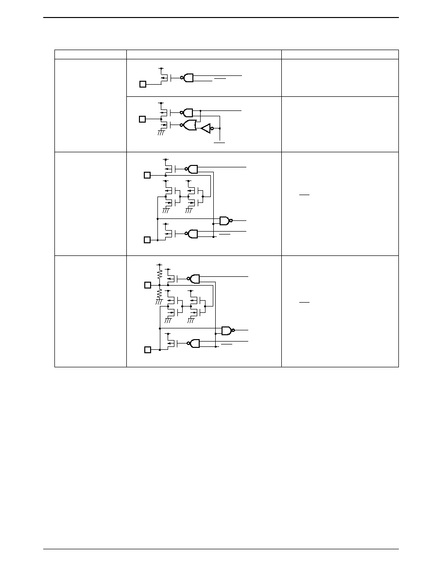
User Options
1. Port 0, 1, 4, 5, and 8 output level at reset option
The output levels at reset for I/O ports 0, 1, 4, 5, and 8, in independent 4-bit groups, can be selected from the
following two options.
2. Oscillator circuit options
∑ Main clock
Note: There is no RC oscillator option.
∑ Sub-clock
3. Watchdog timer option
A runaway detection function (watchdog timer) can be selected as an option.
4. Port output type options
∑ The output type of each bit (pin) in ports P0, P1, P2, P3 (except for the P33/HOLD pin), P4, P5, P6, and PC can be
No. 5489-8/28
LC66P5316
Option
Circuit
Conditions and notes
1. External clock
2. Ceramic oscillator
The input has Schmitt characteristics
Option
Circuit
Conditions and notes
1. Ports PE0 and PE1
2 Sub-oscillator
(crystal oscillator)
Option
Conditions and notes
1. Output high at reset
The four bits of ports 0, 1, 4, 5, or 8 are set in a group
2. Output low at reset
The four bits of ports 0, 1, 4, 5, or 8 are set in a group
Option
Circuit
Conditions and notes
1. Open-drain output
2. Output with built-in pull-up
resistor
The port P2, P3, P5, and P6 inputs have Schmitt
characteristics.
The port P2, P3, P5, and P6 inputs have Schmitt
characteristics.
The CMOS outputs (ports P2, P3, P6, and PC)
and the pull-up MOS outputs (P0, P1, P4, and
P5) are distinguished by the drive capacity of the
p-channel transistor.
OSC1
OSC1
OSC2
C1
C2
Ceramic oscillator
DSB
Input data
XT1
XT2
C1
C2
Crystal oscillator
DSB
Output data
Input data
DSB
Output data
Input data
∑ One of the following two options can be selected for P8, in bit units.
5. Inverter array circuit option
One of the following options can be selected for each of the following port sets: P40/P41, P42/P43, PC2/PC3,
PD0/PD1, and PD2/PD3. (PDs do not use option 1 because they are dedicated to inputs.)
No. 5489-9/28
LC66P5316
Option
Circuit
Conditions and notes
1. Open-drain output
2. Output with built-in pull-
down resistor
(CMOS output)
Option
Circuit
Conditions and notes
1. Normal port I/O circuit
2. Inverter I/O circuit
When the open-drain output type is selected
When the built-in pull-up resistor output type is
selected
The CMOS outputs (PC) and the pull-up MOS
outputs (P4) are distinguished by the drive
capacity of the p-channel transistor.
If this option is selected, the I/O circuit is disabled
by the DSB signal.
Also note that the open-drain port output type
option and the high level at reset option must be
selected.
DSB
Output data
DSB
Output data
DSB
Output data
Input data
DSB
Output data
Input data
DSB
DSB
Output data
high
Input data
Output data
high
Input data
6. Buffer array circuit option
In addition to normal port output, one of the following two options may also be selected for P80 and P81.
No. 5489-10/28
LC66P5316
Option
Circuit
Conditions and notes
1. Normal port output
2. Buffer input (P80) and
buffer output (P81) circuits
3. Buffer input (P80) and
buffer output (P81) circuits
with built-in zero-cross
detection circuits
When the open-drain output type is selected
If this option is selected, the I/O circuit is disabled
by the DSB signal.
Also note that the open-drain port output type
option and the high level at reset option must be
selected.
If this option is selected, the I/O circuit is disabled
by the DSB signal.
Also note that the open-drain port output type
option and the high level at reset option must be
selected.
When the built-in pull-down resistor output type is
selected (CMOS output)
DSB
Output data
DSB
Output data
DSB
P80
P81
Output data
low
Output data
low
DSB
P80
P81
Output data
low
Output data
low

LC665316 Series Option Data Area and Definitions
LC66P5316
ROM area
Bit
Option specified
Option/data relationship
7
P5
Output level at reset
0 = high level, 1 = low level
6
P4
5
Sub-oscillator option
0 = port PE, 1 = crystal oscillator
3FF0H
4
Oscillator option
0 = external clock, 1 = ceramic oscillator
3
P8
2
P1
Output level at reset
0 = low level, 1 = high level
1
P0
0
Watchdog timer option
0 = none, 1 = yes (present)
7
P13
6
P12
Output type
0 = OD, 1 = PU
5
P11
3FF1H
4
P10
3
P03
2
P02
Output type
0 = OD, 1 = PU
1
P01
0
P00
7
Unused
This bit must be set to 0.
6
P32
5
P31
Output type
0 = OD, 1 = PU
3FF2H
4
P30
3
P23
2
P22
Output type
0 = OD, 1 = PU
1
P21
0
P20
7
P53
6
P52
Output type
0 = OD, 1 = PU
5
P51
3FF3H
4
P50
3
P43
2
P42
Output type
0 = OD, 1 = PU
1
P41
0
P40
7
6
Unused
This bit must be set to 0.
5
3FF4H
4
3
P63
2
P62
Output type
0 = OD, 1 = PU
1
P61
0
P60
7
6
Unused
This bit must be set to 0.
5
3FF5H
4
3
P83
2
P82
Output type
0 = OD, 1 = PD
1
P81
0
P80
7
6
Unused
This bit must be set to 0.
5
3FF6H
4
3
2
Unused
This bit must be set to 0.
1
0
Continued on next page.

Continued from preceding page.
No. 5489-12/28
LC66P5316
ROM area
Bit
Option specified
Option/data relationship
7
6
Unused
This bit must be set to 0.
5
3FF7H
4
3
PC3
2
PC2
Output type
0 = OD, 1 = PU
1
PC1
0
PC0
7
Unused
This bit must be set to 1.
6
Buffer output
0 = used, 1 = none
5
Buffer output with zero-cross bias input
0 = used, 1 = none
3FF8H
4
PD3
3
PD1
2
PC3
Inverter output
0 = inverter output, 1 = none
1
P43
0
P41
7
6
Unused
This bit must be set to 0.
5
3FF9H
4
3
2
Unused
This bit must be set to 0.
1
0
7
6
Unused
This bit must be set to 0.
5
3FFAH
4
3
2
Unused
This bit must be set to 0.
1
0
7
6
Unused
This bit must be set to 0.
5
3FFBH
4
3
2
Unused
This bit must be set to 0.
1
0
7
6
Unused
This bit must be set to 0.
5
3FFCH
4
3
2
Unused
This bit must be set to 0.
1
0
7
6
5
3FFDH
4
Reserved. Must be set to predefined data values.
This data is generated by the assembler.
3
If the assembler is not used, set this data to `00'.
2
1
0
Continued on next page.
Continued from preceding page.
Usage Notes
1. Option specification
When using a Sanyo cross assembler with the LC66P5316, use the version called "LC66S.EXE" and specify the
actual microcontroller to be evaluated with the CPU pseudoinstruction in the source file. The port options must be
specified in the source file. The cross assembler will create an options code list in the option specification area
(locations 3FF0H to 3FFFH). It is also possible to directly set up data in the option specification area. If this is done,
the options must be specified according to the option code creation table shown on the following page.
2. Writing the EPROM
Use a special-purpose writing conversion board (the W66EP5316D for the DIP package, and the W66EP5316Q for
the QFP package) to allow the EPROM programmers listed below to be used when writing the data created by the
cross assembler to the LC66P5316.
∑ The EPROM programmers listed below can be used.
∑ The "27512 (V
PP
12.5 V) Intel high-speed write" technique must be used to write the EPROM. Set the address
range to location 0 to 3FFFH. The DASEC jumper must be off.
3. Using the data security function
The data security function sets up the microcontroller in advance so that data that was written to the microcontroller
EPROM cannot be read out.
Use the following procedure to enable the LC66P5316 data security function.
∑ Set the write conversion board DASEC jumper to the on position.
∑ Write the data to the EPROM once again.
At this time, since this function will operate, the EPROM programmer will issue an error. However, this error does
not indicate that there was a problem in either the programmer or the LSI.
Notes: 1. If the data at all addresses was "FF" at step 2, the data security function will not be activated.
Notes:
2. The data security function will not be activated at step 2 if the "blank
program
verify" operation
sequence is used.
Notes:
3. Always return the jumper to the off position after the data security function has been activated.
No. 5489-13/28
LC66P5316
ROM area
Bit
Option specified
Option/data relationship
7
6
5
3FFEH
4
Reserved. Must be set to predefined data values.
This data is generated by the assembler.
3
If the assembler is not used, set this data to `00'.
2
1
0
7
6
5
3FFFH
4
Reserved. Must be set to predefined data values.
This data is generated by the assembler.
3
If the assembler is not used, set this data to `00'.
2
1
0
Manufacturer
Models that can be used
Advantest
R4945, R4944A, R4943, or equivalent products
Ando
AF9704
AVAL
--
Minato Electronics
MODEL1890A
Specifications
Absolute Maximum Ratings
at Ta = 25∞C, V
SS
= 0 V
Note: 1. Applies to pins with open-drain output specifications. For pins with other than open-drain output specifications, the ratings in the pin column for that
pin apply.
2. For the oscillator input and output pins, levels up to the free-running oscillation level are allowed.
3. Sink current (Applies to P8 and PD when either the CMOS output specifications or the inverter array specifications have been selected.)
4. Source current (Applies to all pins except P8 and PD for which the pull-up output specifications, the CMOS output specifications, or the inverter
array specifications have been selected. Applies to PD pins for which the inverter array specifications have been selected.) Contact your Sanyo
representative for the electrical characteristics when the inverter array or buffer array options are specified.
5. We recommend the use of reflow soldering techniques to solder mount QFP packages.
Please consult with your Sanyo representative for details on process conditions if the package itself is to be directly immersed in a solder dip bath
(solder dip or spray techniques).
LC66P5316
Parameter
Symbol
Conditions
Ratings
Unit
Note
Maximum supply voltage
V
DD
max
V
DD
≠0.3 to +7.0
V
V
IN
1
P2, P3 (except for the P33/HOLD pin),
≠0.3 to +7.0
V
1
Input voltage
P61, and P63
V
IN
2
All other inputs
≠0.3 to V
DD
+ 0.3
V
2
V
OUT
1
P2, P3 (except for the P33/HOLD pin),
≠0.3 to +7.0
V
1
Output voltage
P61, and P63
V
OUT
2
All other inputs
≠0.3 to V
DD
+ 0.3
V
2
I
ON
1
P0, P1, P2, P3 (except for the P33/HOLD pin),
20
mA
3
P4, P5, P6, P8, PC, PD1, PD3
Output current per pin
≠I
OP
1
P0, P1, P4, P5
2
mA
4
≠I
OP
2
P2, P3 (except for the P33/HOLD pin),
4
mA
4
P6,P8, and PC
≠I
OP
3
P41, P43, PC3, PD1, PD3, P81
10
mA
4
I
ON
1
P4, P5, P6, P8, PC
75
mA
3
I
ON
2
P0, P1, P2, P3 (except for the P33/HOLD pin),
75
mA
3
Total pin current
PD1, PD3
I
OP
1
P4, P5, P6, P8, PC
25
mA
4
I
OP
2
P0, P1, P2, P3 (except for the P33/HOLD pin),
25
mA
4
PD1, PD3
Allowable power dissipation
Pd max
Ta = ≠30 to +70∞C: DIP48S (QFP48E)
600 (430)
mW
5
Operating temperature
Topr
≠30 to +70
∞C
Storage temperature
Tstg
≠55 to +125
∞C
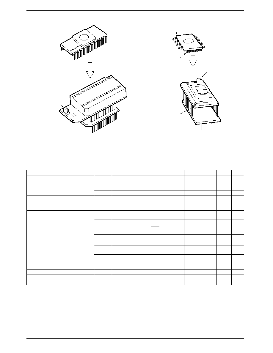
SW DASEC
O
Pin 1
Aligned to the top
SW
DASEC
Cut corner
Pin 1
Pin 1
LC66P5316 (DIP)
LC66P5316 (QFP)
Write board (W66EP5316D)
Write board (W66EP5316Q)

Allowable Operating Ranges
at Ta = ≠30 to +70∞C, V
SS
= 0 V, V
DD
= 4.0 to 5.5 V, unless otherwise specified.
Note: 1. Applies to pins with open-drain specifications. However, V
IH
2 applies to the P33/HOLD pin.
When ports P2, P3, and P6 have CMOS output specifications they cannot be used as input pins.
2. PC port pins with CMOS output specifications cannot be used as input pins.
Contact your Sanyo representative for the allowable operating ranges for P4, PC, and PD when the inverter array is used, and for P8 when the
buffer array is used.
3. Applies to pins with open-drain specifications. However, V
IL
2 applies to the P33/HOLD pin.
P2, P3, and P6 port pins with CMOS output specifications cannot be used as input pins.
No. 5489-15/28
LC66P5316
Parameter
Symbol
Conditions
min
typ
max
Unit
Note
Operating supply voltage
V
DD
V
DD
4.0
5.5
V
Memory retention supply voltage
V
DD
H
V
DD
: During hold mode
1.8
5.5
V
V
IH
1
P2, P3 (except for the P33/HOLD pin),
0.8 V
DD
+7.0
V
1
P61, and P63: N-channel output transistor off
Input high-level voltage
V
IH
2
P33/HOLD, RES, OSC1:
0.8 V
DD
V
DD
V
N-channel output transistor off
V
IH
3
P0, P1, P4, P5, PC, PD, PE:
0.8 V
DD
V
DD
V
2
N-channel output transistor off
V
IL
1
P2, P3 (except for the P33/HOLD pin), P6,
V
SS
0.2 V
DD
V
RES, and OSC1: N-channel output transistor off
Input low-level voltage
V
IL
2
P33/HOLD: V
DD
= 1.8 to 5.5 V
V
SS
0.2 V
DD
V
V
IL
3
P0, P1, P4, P5, PC, PD, PE, TEST:
V
SS
0.2 V
DD
V
2
N-channel output transistor off
When the main oscillator is operating
0.4
4.20
MHz
Operating frequency
fop
(10)
(0.95)
(µs)
(instruction cycle time)
(Tcyc)
When the sub-oscillator is operating
30
32.768
100
kHz
(133.2)
(122)
(40)
(µs)
[External clock input conditions]
OSC1: Defined by Figure 1. Input the clock
Frequency
f
ext
signal to OSC1 and leave OSC2 open.
0.4
4.20
MHz
(External clock input must be selected as the
oscillator circuit option.)
OSC1: Defined by Figure 1. Input the clock
Pulse width
t
extH
, t
extL
signal to OSC1 and leave OSC2 open.
100
ns
(External clock input must be selected as the
oscillator circuit option.)
OSC1: Defined by Figure 1. Input the clock
Rise and fall times
t
extR
, t
extF
signal to OSC1 and leave OSC2 open.
30
ns
(External clock input must be selected as the
oscillator circuit option.)
Electrical Characteristics
at Ta = ≠30 to +70∞C, V
SS
= 0 V, V
DD
= 4.0 to 5.5 V unless otherwise specified.
LC66P5316
Parameter
Symbol
Conditions
min
typ
max
Unit
Note
P2, P3 (except for the P33/HOLD pin),
I
IH
1
P61, and P63: V
IN
= +10.0 V, with the output
5.0
µA
1
Nch transistor off
P0, P1, P4, P5, P6, PC, OSC1, and P33/HOLD
I
IH
2
(Does not apply to PD, PE, PC2, and PC3):
1.0
µA
1
V
IN
= V
DD
, with the output Nch transistor off
Input high-level current
PD, PC2, PC3, PE0, (When used as a port; does
I
IH
3
not apply when the sub-oscillator option is
1.0
µA
1
selected.): V
IN
= V
DD
, with the output Nch
transistor off
I
IH
4
RES: V
IN
= V
DD
, operating, halt mode
10
µA
1
I
IH
5
RES: V
IN
= V
DD
, hold mode
1.0
µA
1
I
IH
6
PE1 (When used as a port; does not apply when
1.0
µA
1
the sub-oscillator option is selected.) : V
IN
= V
DD
I
IL
1
Input ports other than PD, PE, PC2, and PC3:
≠1.0
µA
2
V
IN
= V
SS
, with the output Nch transistor off
I
IL
2
PD, PC2, PC3, PE0: V
IN
= V
SS
,
≠1.0
µA
2
Input low-level current
with the output Nch transistor off
I
IL
3
RES: V
IN
= V
SS
100
µA
1
PE1 (When used as a port; does not apply
I
IL
4
when the sub-oscillator option is selected.):
20
µA
1
V
IN
= V
SS
P2, P3 (except for the P33/HOLD pin),
V
DD
≠ 1.0
Output high-level voltage
V
OH
1
P6, P8, and PC: I
OH
= ≠1 mA
V
3
P2, P3 (except for the P33/HOLD pin),
V
DD
≠ 0.5
P6, P8, and PC: I
OH
= ≠0.1 mA
Value of the output pull-up resistor
R
PO
P0, P1, P4, P5
30
100
150
k
4
V
OL
1
P0, P1, P2, P3, P4, P5, P6, P8, and PC
0.4
V
5
Output low-level voltage
(except for the P33/HOLD pin): I
OL
= 1.6 mA
V
OL
2
P0, P1, P2, P3, P4, P5, P6, P8, and PC
1.5
V
(except for the P33/HOLD pin): I
OL
= 8 mA
I
OFF
1
P2, P3, P61, P63: V
IN
= +7.0 V
5.0
µA
6
Output off leakage current
I
OFF
2
Does not apply to P2, P3, P61, P63, and P8.:
1.0
µA
6
V
IN
= V
DD
I
OFF
3
P8: V
IN
= V
SS
≠1.0
µA
7
[Schmitt characteristics]
Hysteresis voltage
V
HYS
0.1 V
DD
V
High-level threshold voltage
Vt H
P2, P3, P5, P6, OSC1 (EXT), RES
0.5 V
DD
0.8 V
DD
V
Low-level threshold voltage
Vt L
0.2 V
DD
0.5 V
DD
V
[Ceramic oscillator]
Oscillator frequency
f
CF
OSC1, OSC2: Figure 2, 4 MHz
4.0
MHz
Oscillator stabilization time
f
CFS
Figure 3, 4 MHz
10.0
ms
[Crystal oscillator]
Oscillator frequency
f
XT
XT1, XT2: Figure 2, when the sub-oscillator
32.768
kHz
option is selected, 32 kHz
Oscillator stabilization time
f
XTS
Figure 3, when the sub-oscillator option is
1.0
5.0
s
selected, 32 kHz
[Serial clock]
Cycle time
Input
t
CKCY
0.9
µs
Output
2.0
Tcyc
Low-level and high-level Input
t
CKL
0.4
µs
pulse widths
Output
t
CKH
1.0
Tcyc
Rise an fall times
Output
t
CKR
, t
CKF
0.1
µs
[Serial input]
Data setup time
t
ICK
0.3
µs
Data hold time
t
CKI
0.3
µs
[Serial output]
SO0, SO1: With the timing of Figure 5 and
Output delay time
t
CKO
the test load of Figure 5. Stipulated with respect
0.3
µs
to the falling edge (
) of SCK0 or SCK1.
SI0, SI1: With the timing of Figure 4.
Stipulated with respect to the rising edge (
) of
SCK0 or SCK1.
SCK0, SCK1: With the timing of Figure 4 and
the test load of Figure 5.
Continued on next page.
Continued from preceding page.
Note: 1. With the output Nch transistor off in shared I/O ports with the open-drain output specifications. These pins cannot be used as input pins if the
CMOS output specifications are selected.When the port option is selected for PE.
2. With the output Nch transistor off in shared I/O ports with the open-drain output specifications. The rating for the pull-up output specification pins is
stipulated in terms of the output pull-up current IPO. These pins cannot be used as input pins if the CMOS output specifications are selected.
3. With the output Nch transistor off for CMOS output specification pins. (Also applies when the Pch open-drain option is selected for P8.)
4. With the output Nch transistor off for pull-up output specification pins.
5. When CMOS output specifications are selected for P8.
6. With the output Nch transistor off for open-drain output specification pins.
7. With the output Pch transistor off for open-drain output specification pins.
8. Reset state
Comparator Characteristics
at Ta = ≠30 to +70∞C, V
SS
= 0 V
Note: 1. Does not include the quantization error.
Figure 1 External Clock Input Waveform
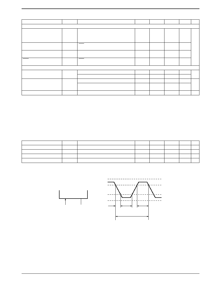
No. 5489-17/28
LC66P5316
Parameter
Symbol
Conditions
min
typ
max
Unit
Note
[Pulse conditions]
INT0: Figure 6, conditions under which the INT0
INT0 high and low-level
t
IOH
, t
IOL
interrupt can be accepted, conditions under
2
Tcyc
which the timer 0 event counter or pulse width
measurement input can be accepted
High and low-level pulse widths
t
IIH
, t
IIL
INT1, INT2: Figure 6, conditions under which
2
Tcyc
for interrupt inputs other than INT0
the corresponding interrupt can be accepted
PIN1 high and low-level
t
PINH
, t
PINL
PIN1: Figure 6, conditions under which the
2
Tcyc
pulse widths
timer 1 event counter input can be accepted
RES high and low-level
t
RSH
, t
RSL
RES: Figure 6, conditions under which reset
3
Tcyc
pulse widths
can be applied.
Operating current drain
I
DD OP
V
DD
: 4-MHz ceramic oscillator
6.0
12
mA
8
V
DD
: 4-MHz external clock
6.0
12
mA
V
DD
: 4-MHz ceramic clock
4.0
8
mA
Halt mode current drain
I
DDHALT
V
DD
: 32 kHz (main oscillator stopped),
100
500
µA
sub-oscillator: crystal
Hold mode current drain
I
DDHOLD
V
DD
: V
DD
= 1.8 to 5.5 V
0.01
10
µA
Parameter
Symbol
Conditions
min
typ
max
Unit
Note
Absolute precision
V
CECM
AN1 to AN4: V
DD
= 4.0 to 5.5 V
±1/2
±1
LSB
1
Threshold voltage
V
THCM
V
DD
= 4.0 to 5.5 V
V
SS
V
DD
V
Input voltage
V
INCM
AN1 to AN4: V
DD
= 4.0 to 5.5 V
V
SS
V
DD
V
Conversion time
T
CCM
V
DD
= 4.0 to 5.5 V
30
µs
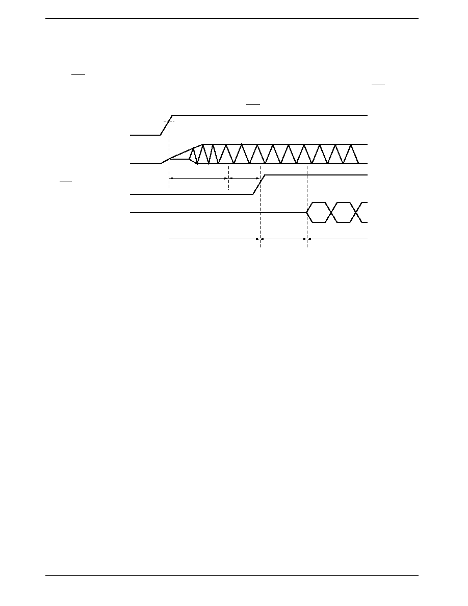
textL
OPEN
(OSC2)
OSC1
textR
textF
VSS
VDD
0.2VDD
0.8VDD
1/fext
textH
External clock
Figure 2 Ceramic Oscillator Circuit
Figure 3 Oscillator Stabilization Period
Table 1 Guaranteed Ceramic Oscillator Constants External capacitor type
Table 2 Guaranteed Crystal Oscillator Constants
Figure 4 Serial I/O Timing
Figure 5 Timing Load
Figure 6 Input Timing for the INT0, INT1, INT2, PIN1, and RES pins
No. 5489-18/28
LC66P5316
External capacitor type
Built-in capacitor type
4 MHz
C1 = 33 pF ± 10%
4 MHz
(Murata Mfg. Co., Ltd.)
C2 = 33 pF ± 10%
(Murata Mfg. Co., Ltd.)
Rd = 220 ± 5%
CSA4.00MG
Rd = 220 ± 5%
CST4.00MG
4 MHz
C1 = 33 pF ± 10%
4 MHz
(Kyocera Corporation)
C2 = 33 pF ± 10%
(Kyocera Corporation)
KBR4.0MS
Rd = 0
KBR4.0MES
32 kHz
C1 = 18 pF ± 10%
(Seiko Epson)
C2 = 18 pF ± 10%
C-002RX
Rd = 470 k ± 5%
OSC2
OSC1
C1
C2
Rd
XT2
Crystal
oscillator
XT1
C1
C2
Rd
Ceramic
oscillator
VDD
OSC
0V
Oscillator
unstable period
tCFS
Stable oscillation
Operating VDD
minimum value
tICK tCKI
tCKL
tCKR
tCKCY
tCKH
tCKF
0.8VDD (input)
VDD-1 (output)
0.2VDD (input)
SCK0
SCK1
SI0
SI1
SO0
SO1
0.4VDD (output)
0.8VDD
0.2VDD
tCK0
VDD-1
0.4VDD
C=50pF
TEST
point
R=1k
tI0H
tI1H
tPINH
tRSH
tI0L
tI1L
tPINL
tRSL
0.8VDD
0.2VDD
No. 5489-19/28
LC66P5316
Preconditions for mounting one-time programmable microprocessors
Usage Notes
Due to inherent structural considerations, it is impossible to fully test one-time programmable microprocessors before
the PROM has been programmed, i.e. before shipment from the factory. We recommend that users screen products
whose PROM has been written according to the following procedure to improve the reliability of these products.
∑ Due to the nature of the product, it is not possible to test write operations to all bits in one-time programmable
microprocessors whose PROM has not been written. Therefore it may be impossible to guarantee a 100% yield on
writing to these products. Please understand that no such guarantee may be made.
∑ Storage of products in the moisture-proof packed (unopened) state
∑ Store products in moisture-proof packages in an environment in which the temperature is no higher than 30∞C and
the relative humidity is no higher than 70%.
∑ Storage of products after opening the moisture-proof packaging
∑ After opening products that were packed in moisture-proof packaging, mount (solder) those products as soon as
possible. Store products for no more than 96 hours after opening the moisture-proof packaging in an environment
in which the temperature is no higher than 30∞C and the relative humidity is no higher than 70%.
a. Preconditions for mounting products that were programmed by the user
b. Preconditions for mounting products that were programmed by Sanyo
Sanyo ROM writing service
Sanyo provides a for-fee ROM writing service that includes writing the one-time programmable ROM, printing,
screening, and read-out verification. Contact your Sanyo sales representative for details.
DIP/QFP product
Mounting
Mounting
Programming and verification
Recommended screening conditions
High-temperature bake (disconnected)
150
∞
C ±5
∞
C, 24 HR
+1HR
≠0HR
Program data verification
DIP/QFP product

LC66XXXX Series Instruction Table (by function)
Abbreviations:
AC:
Accumulator
E:
E register
CF:
Carry flag
ZF:
Zero flag
HL:
Data pointer DPH, DPL
XY:
Data pointer DPX, DPY
M:
Data memory
M (HL):
Data memory pointed to by the DPH, DPL data pointer
M (XY):
Data memory pointed to by the DPX, DPY auxiliary data pointer
M2 (HL): Two words of data memory (starting on an even address) pointed to by the DPH, DPL data pointer
SP:
Stack pointer
M2 (SP): Two words of data memory pointed to by the stack pointer
M4 (SP): Four words of data memory pointed to by the stack pointer
in:
n bits of immediate data
t2:
Bit specification
PCh:
Bits 8 to 11 in the PC
PCm:
Bits 4 to 7 in the PC
PCl:
Bits 0 to 3 in the PC
Fn:
User flag, n = 0 to 15
TIMER0: Timer 0
TIMER1: Timer 1
SIO:
Serial register
P:
Port
P (i4):
Port indicated by 4 bits of immediate data
INT:
Interrupt enable flag
( ), [ ]:
Indicates the contents of a location
:
Transfer direction, result
:
Exclusive or
:
Logical and
:
Logical or
+:
Addition
≠:
Subtraction
--:
Taking the one's complement
No. 5489-20/28
LC66P5316
t2
11
10
01
00
Bit
2
3
2
2
2
1
2
0
No. 5489-21/28
LC66P5316
Continued on next page.
Instruction code
Affected
Mnemonic
Operation
Description
status
Note
D
7
D
6
D
5
D
4
D
3
D
2
D
1
D
0
bits
[Accumulator manipulation instructions]
CLA
Clear AC
1 0 0 0
0 0 0 0
1
1
AC
0
Clear AC to 0.
ZF
Has a vertical
(Equivalent to LAI 0.)
skip function.
DAA
Decimal adjust AC
1 1 0 0
1 1 1 1
2
2
AC
(AC) + 6
Add six to AC.
ZF
in addition
0 0 1 0
0 1 1 0
(Equivalent to ADI 6.)
Decimal adjust AC
1 1 0 0
1 1 1 1
AC
(AC) + 10
DAS
in subtraction
0 0 1 0
1 0 1 0
2
2
(Equivalent to
Add 10 to AC.
ZF
ADI 0AH.)
CLC
Clear CF
0 0 0 1
1 1 1 0
1
1
CF
0
Clear CF to 0.
CF
STC
Set CF
0 0 0 1
1 1 1 1
1
1
CF
1
Set CF to 1.
CF
CMA
Complement AC
0 0 0 1
1 0 0 0
1
1
AC
(AC)
Take the one's complement
ZF
of AC.
IA
Increment AC
0 0 0 1
0 1 0 0
1
1
AC
(AC) + 1
Increment AC.
ZF, CF
DA
Decrement AC
0 0 1 0
0 1 0 0
1
1
AC
(AC) ≠ 1
Decrement AC.
ZF, CF
Rotate AC right
AC
3
(CF),
RAR
through CF
0 0 0 1
0 0 0 0
1
1
ACn
(ACn + 1),
Shift AC (including CF) right.
CF
CF
(AC
0
)
Rotate AC left
AC
0
(CF),
RAL
through CF
0 0 0 0
0 0 0 1
1
1
ACn + 1
(ACn),
Shift AC (including CF) left.
CF, ZF
CF
(AC
3
)
TAE
Transfer AC to E
0 1 0 0
0 1 0 1
1
1
E
(AC)
Transfer the contents of AC to E.
TEA
Transfer E to AC
0 1 0 0
0 1 1 0
1
1
AC
(E)
Transfer the contents of E to AC.
ZF
XAE
Exchange AC with E
0 1 0 0
0 1 0 0
1
1
(AC)
(E)
Exchange the contents of
AC and E.
[Memory manipulation instructions]
IM
Increment M
0 0 0 1
0 0 1 0
1
1
M (HL)
Increment M (HL).
ZF, CF
[M (HL)] + 1
DM
Decrement M
0 0 1 0
0 0 1 0
1
1
M (HL)
Decrement M (HL).
ZF, CF
[M (HL)] ≠ 1
IMDR i8
Increment M direct
1 1 0 0
0 1 1 1
2
2
M (i8)
[M (i8)] + 1
Increment M (i8).
ZF, CF
I
7
I
6
I
5
I
4
I
3
I
2
I
1
I
0
DMDR i8 Decrement M direct
1 1 0 0
0 0 1 1
2
2
M (i8)
[M (i8)] ≠ 1
Decrement M (i8).
ZF, CF
I
7
I
6
I
5
I
4
I
3
I
2
I
1
I
0
SMB t2
Set M data bit
0 0 0 0
1 1 t
1
t
0
1
1
[M (HL), t2]
1
Set the bit in M (HL) specified
by t0 and t1 to 1.
RMB t2
Reset M data bit
0 0 1 0
1 1 t
1
t
0
1
1
[M (HL), t2]
0
Clear the bit in M (HL)
ZF
specified by t0 and t1 to 0.
[Arithmetic, logic and comparison instructions]
Add the contents of AC and
AD
Add M to AC
0 0 0 0
0 1 1 0
1
1
AC
(AC) +
M (HL) as two's complement
ZF, CF
[M (HL)]
values and store the result
in AC.
Add the contents of AC and
ADDR i8 Add M direct to AC
1 1 0 0
1 0 0 1
2
2
AC
(AC) + [M (i8)]
M (i8) as two's complement
ZF, CF
I
7
I
6
I
5
I
4
I
3
I
2
I
1
I
0
values and store the result
in AC.
Add the contents of AC,
ADC
Add M to AC with CF
0 0 0 0
0 0 1 0
1
1
AC
(AC) +
M (HL) and C as two's
ZF, CF
[M (HL)] + (CF)
complement values and
store the result in AC.
Add the contents of AC and
ADI i4
Add immediate data
1 1 0 0
1 1 1 1
2
2
AC
(AC) +
the immediate data as two's
ZF
to AC
0 0 1 0
I
3
I
2
I
1
I
0
I
3
, I
2
, I
1
, I
0
complement values and store
the result in AC.
Subtract the contents of AC
CF will be zero if
SUBC
Subtract AC from M
0 0 0 1
0 1 1 1
1
1
AC
[M (HL)] ≠
and CF from M (HL) as two's
ZF, CF
there was a
with CF
(AC) ≠ (CF)
complement values and store
borrow and one
the result in AC.
otherwise.
And M with AC then
AC
(AC)
Take the logical and of AC
ANDA
store AC
0 0 0 0
0 1 1 1
1
1
[M (HL)]
and M (HL) and store the
ZF
result in AC.
Or M with AC then
AC
(AC)
Take the logical or of AC and
ORA
store AC
0 0 0 0
0 1 0 1
1
1
[M (HL)]
M (HL) and store the result
ZF
in AC.
Number of
bytes
Number of
cycles
Continued from preceding page.
No. 5489-22/28
LC66P5316
Continued on next page.
Instruction code
Affected
Mnemonic
Operation
Description
status
Note
D
7
D
6
D
5
D
4
D
3
D
2
D
1
D
0
bits
[Arithmetic, logic and comparison instructions]
Exclusive or M with
AC
(AC)
Take the logical exclusive or
EXL
AC then store AC
0 0 0 1
0 1 0 1
1
1
[M (HL)]
of AC and M (HL) and store
ZF
the result in AC.
And M with AC then
M (HL)
(AC)
Take the logical and of AC
ANDM
store M
0 0 0 0
0 0 1 1
1
1
[M (HL)]
and M (HL) and store the
ZF
result in M (HL).
Or M with AC then
M (HL)
(AC)
Take the logical or of AC and
ORM
store M
0 0 0 0
0 1 0 0
1
1
[M (HL)]
M (HL) and store the result
ZF
in M (HL).
Compare the contents of AC
and M (HL) and set or clear CF
and ZF according to the result.
CM
Compare AC with M
0 0 0 1
0 1 1 0
1
1
[M (HL)] + (AC) + 1
ZF, CF
Compare the contents of AC
and the immediate data
I
3
I
2
I
1
I
0
and set or clear CF
and ZF according to the result.
CI i4
Compare AC with
1 1 0 0
1 1 1 1
2
2
I
3
I
2
I
1
I
0
+ (AC) + 1
ZF, CF
immediate data
1 0 1 0
I
3
I
2
I
1
I
0
ZF
1
Compare the contents of DP
L
CLI i4
Compare DP
L
with
1 1 0 0
1 1 1 1
2
2
if (DP
L
) = I
3
I
2
I
1
I
0
with the immediate data.
ZF
immediate data
1 0 1 1
I
3
I
2
I
1
I
0
ZF
0
Set ZF if identical and clear
if (DP
L
) I
3
I
2
I
1
I
0
ZF if not.
ZF
1
if (AC, t2) = [M (HL), Compare the corresponding
CMB t2
Compare AC bit with
1 1 0 0
1 1 1 1
2
2
t2]
bits specified by t0 and t1 in
ZF
M data bit
1 1 0 1
0 0 t
1
t
0
ZF
0
AC and M (HL). Set ZF if
if (AC, t2) [M (HL),
identical and clear ZF if not.
t2]
[Load and store instructions]
LAE
Load AC and E from
0 1 0 1
1 1 0 0
1
1
AC
M (HL),
Load the contents of M2 (HL)
M2 (HL)
E
M (HL + 1)
into AC, E.
LAI i4
Load AC with
1 0 0 0
I
3
I
2
I
1
I
0
1
1
AC
I
3
I
2
I
1
I
0
Load the immediate data
ZF
Has a vertical
immediate data
into AC.
skip function
LADR i8
Load AC from M
1 1 0 0
0 0 0 1
2
2
AC
[M (i8)]
Load the contents of M (i8)
ZF
direct
I
7
I
6
I
5
I
4
I
3
I
2
I
1
I
0
into AC.
S
Store AC to M
0 1 0 0
0 1 1 1
1
1
M (HL)
(AC)
Store the contents of AC into
M (HL).
SAE
Store AC and E to
0 1 0 1
1 1 1 0
1
1
M (HL)
(AC)
Store the contents of AC, E
M2 (HL)
M (HL + 1)
(E)
into M2 (HL).
Load the contents of M (reg)
into AC.
The reg is either HL or XY
Load AC from
depending on t
0
.
LA reg
M (reg)
0 1 0 0
1 0 t
0
0
1
1
AC
[M (reg)]
ZF
Number of
bytes
Number of
cycles
Magnitude
CF ZF
comparison
[M (HL)] > (AC)
0
0
[M (HL)] = (AC)
1
1
[M (HL)] < (AC)
1
0
Magnitude
CF ZF
comparison
I
3
I
2
I
1
I
0
> AC
0
0
I
3
I
2
I
1
I
0
= AC
1
1
I
3
I
2
I
1
I
0
< AC
1
0
reg
T
0
HL
0
XY
1

Continued from preceding page.
No. 5489-23/28
LC66P5316
Continued on next page.
Instruction code
Affected
Mnemonic
Operation
Description
status
Note
D
7
D
6
D
5
D
4
D
3
D
2
D
1
D
0
bits
[Load and store instructions]
Load the contents of M (reg)
into AC. (The reg is either HL
ZF is set
Load AC from M (reg)
AC
[M (reg)]
or XY.) Then increment the
according to the
LA reg, I
then increment reg
0 1 0 0
1 0 t
0
1
1
2
DP
L
(DP
L
) + 1
contents of either DP
L
or DP
Y
. ZF
result of
or DP
Y
(DP
Y
) + 1
The relationship between t
0
incrementing
and reg is the same as that
DP
L
or DP
Y
.
for the LA reg instruction.
Load the contents of M (reg)
into AC. (The reg is either HL
ZF is set
Load AC from M (reg)
AC
[M (reg)]
or XY.) Then decrement the
according to the
LA reg, D
then decrement reg
0 1 0 1
1 0 t
0
1
1
2
DP
L
(DP
L
) ≠ 1
contents of either DP
L
or DP
Y
. ZF
result of
or DP
Y
(DP
Y
) ≠ 1
The relationship between t
0
decrementing
and reg is the same as that
DP
L
or DP
Y
.
for the LA reg instruction.
Exchange the contents of
M (reg) and AC.
The reg is either HL or XY
Exchange AC with
depending on t
0
.
XA reg
M (reg)
0 1 0 0
1 1 t
0
0
1
1
(AC)
[M (reg)]
Exchange the contents of
M (reg) and AC. (The reg is
ZF is set
Exchange AC with
(AC)
[M (reg)]
either HL or XY.) Then
according to the
XA reg, I M (reg) then
0 1 0 0
1 1 t
0
1
1
2
DP
L
(DP
L
) + 1
increment the contents of
ZF
result of
increment reg
or DP
Y
(DP
Y
) + 1
either DP
L
or DP
Y
. The
incrementing
relationship between t
0
and
DP
L
or DP
Y
.
reg is the same as that for
the XA reg instruction.
Exchange the contents of
M (reg) and AC. (The reg is
ZF is set
Exchange AC with
(AC)
[M (reg)]
either HL or XY.) Then
according to the
XA reg, D M (reg) then
0 1 0 1
1 1 t
0
1
1
2
DP
L
(DP
L
) ≠ 1
decrement the contents of
ZF
result of
decrement reg
or DP
Y
(DP
Y
) ≠ 1
either DP
L
or DP
Y
. The
decrementing
relationship between t
0
and
DP
L
or DP
Y
.
reg is the same as that for
the XA reg instruction.
XADR i8
Exchange AC with
1 1 0 0
1 0 0 0
2
2
(AC)
[M (i8)]
Exchange the contents of AC
M direct
I
7
I
6
I
5
I
4
I
3
I
2
I
1
I
0
and M (i8).
LEAI i8
Load E & AC with
1 1 0 0
0 1 1 0
2
2
E
I
7
I
6
I
5
I
4
Load the immediate data i8
immediate data
I
7
I
6
I
5
I
4
I
3
I
2
I
1
I
0
AC
I
3
I
2
I
1
I
0
into E, AC.
Load into E, AC the ROM data
RTBL
Read table data from
0 1 0 1
1 0 1 0
1
2
E, AC
at the location determined by
program ROM
[ROM (PCh, E, AC)]
replacing the lower 8 bits of
the PC with E, AC.
Output from ports 4 and 5 the
Read table data from
Port 4, 5
ROM data at the location
RTBLP
program ROM then
0 1 0 1
1 0 0 0
1
2
[ROM (PCh, E, AC)]
determined by replacing the
output to P4, 5
lower 8 bits of the PC with
E, AC.
[Data pointer manipulation instructions]
Load DP
H
with zero
LDZ i4
and DP
L
with
0 1 1 0
I
3
I
2
I
1
I
0
1
1
DP
H
0
Load zero into DP
H
and the
immediate data
DPL
I
3
I
2
I
1
I
0
immediate data i4 into DP
L
.
respectively
LHI i4
Load DP
H
with
1 1 0 0
1 1 1 1
2
2
DP
H
I
3
I
2
I
1
I
0
Load the immediate data i4
immediate data
0 0 0 0
I
3
I
2
I
1
I
0
into DP
H
.
LLI i4
Load DP
L
with
1 1 0 0
1 1 1 1
2
2
DP
L
I
3
I
2
I
1
I
0
Load the immediate data i4
immediate data
0 0 0 1
I
3
I
2
I
1
I
0
into DP
L
.
LHLI i8
Load DP
H
, DP
L
with
1 1 0 0
0 0 0 0
2
2
DP
H
I
7
I
6
I
5
I
4
Load the immediate data into
immediate data
I
7
I
6
I
5
I
4
I
3
I
2
I
1
I
0
DP
L
I
3
I
2
I
1
I
0
DL
H
, DP
L
.
LXYI i8
Load DP
X
, DP
Y
with
1 1 0 0
0 0 0 0
2
2
DP
X
I
7
I
6
I
5
I
4
Load the immediate data into
immediate data
I
7
I
6
I
5
I
4
I
3
I
2
I
1
I
0
DP
Y
I
3
I
2
I
1
I
0
DL
X
, DP
Y
.
Number of
bytes
Number of
cycles
reg
T
0
HL
0
XY
1
Continued from preceding page.
No. 5489-24/28
LC66P5316
Continued on next page.
Instruction code
Affected
Mnemonic
Operation
Description
status
Note
D
7
D
6
D
5
D
4
D
3
D
2
D
1
D
0
bits
[Data pointer manipulation instructions]
IL
Increment DP
L
0 0 0 1
0 0 0 1
1
1
DP
L
(DP
L
) + 1
Increment the contents
ZF
of DP
L
.
DL
Decrement DP
L
0 0 1 0
0 0 0 1
1
1
DP
L
(DP
L
) ≠ 1
Decrement the contents
ZF
of DP
L
.
IY
Increment DP
Y
0 0 0 1
0 0 1 1
1
1
DP
Y
(DP
Y
) + 1
Increment the contents
ZF
of DP
Y
.
DY
Decrement DP
Y
0 0 1 0
0 0 1 1
1
1
DP
Y
(DP
Y
) ≠ 1
Decrement the contents
ZF
of DP
Y
.
TAH
Transfer AC to DP
H
1 1 0 0
1 1 1 1
2
2
DP
H
(AC)
Transfer the contents of AC
1 1 1 1
0 0 0 0
to DP
H
.
THA
Transfer DP
H
to AC
1 1 0 0
1 1 1 1
2
2
AC
(DP
H
)
Transfer the contents of DP
H
ZF
1 1 1 0
0 0 0 0
to AC.
XAH
Exchange AC
0 1 0 0
0 0 0 0
1
1
(AC)
(DP
H
)
Exchange the contents of AC
with DP
H
and DP
H
.
TAL
Transfer AC to DP
L
1 1 0 0
1 1 1 1
2
2
DP
L
(AC)
Transfer the contents of AC
1 1 1 1
0 0 0 1
to DP
L
.
TLA
Transfer DP
L
to AC
1 1 0 0
1 1 1 1
2
2
AC
(DP
L
)
Transfer the contents of DP
L
ZF
1 1 1 0
0 0 0 1
to AC.
XAL
Exchange AC
0 1 0 0
0 0 0 1
1
1
(AC)
(DP
L
)
Exchange the contents of AC
with DP
L
and DP
L
.
TAX
Transfer AC to DP
X
1 1 0 0
1 1 1 1
2
2
DP
X
(AC)
Transfer the contents of AC
1 1 1 1
0 0 1 0
to DP
X
.
TXA
Transfer DP
X
to AC
1 1 0 0
1 1 1 1
2
2
AC
(DP
X
)
Transfer the contents of DP
X
ZF
1 1 1 0
0 0 1 0
to AC.
XAX
Exchange AC
0 1 0 0
0 0 1 0
1
1
(AC)
(DP
X
)
Exchange the contents of AC
with DP
X
and DP
X
.
TAY
Transfer AC to DP
Y
1 1 0 0
1 1 1 1
2
2
DP
Y
(AC)
Transfer the contents of AC
1 1 1 1
0 0 1 1
to DP
Y
.
TYA
Transfer DP
Y
to AC
1 1 0 0
1 1 1 1
2
2
AC
(DP
Y
)
Transfer the contents of DP
Y
ZF
1 1 1 0
0 0 1 1
to AC.
XAY
Exchange AC
0 1 0 0
0 0 1 1
1
1
(AC)
(DP
Y
)
Exchange the contents of AC
with DP
Y
and DP
Y
.
[Flag manipulation instructions]
SFB n4
Set flag bit
0 1 1 1
n
3
n
2
n
1
n
0
1
1
Fn
1
Set the flag specified
by n4 to 1.
RFB n4
Reset flag bit
0 0 1 1
n
3
n
2
n
1
n
0
1
1
Fn
0
Reset the flag specified
ZF
by n4 to 0.
[Jump and subroutine instructions]
PC13, 12
This becomes
JMP
Jump in the current
1 1 1 0 P
11
P
10
P
9
P
8
PC13, 12
Jump to the location in the
PC12 + (PC12)
addr
bank
P
7
P
6
P
5
P
4
P
3
P
2
P
1
P
0
2
2
PC11 to 0
same bank specified by the
immediately
P
11
to P
8
immediate data P12.
following a BANK
instruction.
Jump to the address
PC13 to 8
Jump to the location
JPEA
stored at E and AC
0 0 1 0
0 1 1 1
1
1
PC13 to 8,
determined by replacing the
in the current page
PC7 to 4
(E),
lower 8 bits of the PC
PC3 to 0
(AC)
by E, AC.
PC13 to 11
0,
PC10 to 0
CAL
Call subroutine
0 1 0 1
0 P
10
P
9
P
8
2
2
P
10
to P
0
,
Call a subroutine.
addr
P
7
P
6
P
5
P
4
P
3
P
2
P
1
P
0
M4 (SP)
(CF, ZF, PC13 to 0),
SP
(SP)-4
PC13 to 6,
PC10
0,
CZP
Call subroutine in the
1 0 1 0
P
3
P
2
P
1
P
0
1
2
PC5 to 2
P
3
to P
0
, Call a subroutine on page 0
addr
zero page
M4 (SP)
in bank 0.
(CF, ZF, PC12 to 0),
SP
SP-4
BANK
Change bank
0 0 0 1
1 0 1 1
1
1
Change the memory bank
and register bank.
Number of
bytes
Number of
cycles
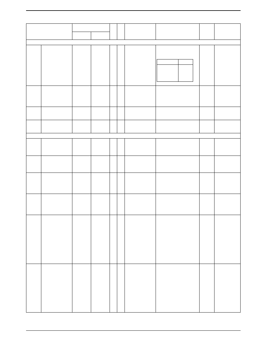
Continued from preceding page.
No. 5489-25/28
LC66P5316
Instruction code
Affected
Mnemonic
Operation
Description
status
Note
D
7
D
6
D
5
D
4
D
3
D
2
D
1
D
0
bits
[Jump and subroutine instructions]
Store the contents of reg in
M2 (SP). Subtract 2 from SP
after the store.
PUSH
Push reg on M2 (SP)
1 1 0 0
1 1 1 1
2
2
M2 (SP)
(reg)
reg
1 1 1 1
1 i
1
i
0
0
SP
(SP) ≠ 2
Add 2 to SP and then load the
POP
1 1 0 0
1 1 1 1
SP
(SP) + 2
contents of M2(SP) into reg.
reg
Pop reg off M2 (SP)
1 1 1 0
1 i
1
i
0
0
2
2
reg
[M2 (SP)]
The relation between i1i0 and
reg is the same as that for the
PUSH reg instruction.
Return from
SP
(SP) + 4
Return from a subroutine or
RT
subroutine
0 0 0 1
1 1 0 0
1
2
PC
[M4 (SP)]
interrupt handling routine. ZF
and CF are not restored.
Return from interrupt
SP
(SP) + 4
Return from a subroutine or
RTI
routine
0 0 0 1
1 1 0 1
1
2
PC
[M4 (SP)]
interrupt handling routine. ZF
ZF, CF
CF, ZF
[M4 (SP)]
and CF are restored.
[Branch instructions]
PC7 to 0
Branch to the location in the
BAt2
Branch on AC bit
1 1 0 1
0 0 t
1
t
0
2
2
P
7
P
6
P
5
P
4
same page specified by P
7
to
addr
P
7
P
6
P
5
P
4
P
3
P
2
P
1
P
0
P
3
P
2
P
1
P
0
P
0
if the bit in AC specified by
if (AC, t2) = 1
the immediate data t
1
t
0
is one.
PC7 to 0
Branch to the location in the
BNAt2
Branch on no AC bit
1 0 0 1
0 0 t
1
t
0
2
2
P
7
P
6
P
5
P
4
same page specified by P
7
to
addr
P
7
P
6
P
5
P
4
P
3
P
2
P
1
P
0
P
3
P
2
P
1
P
0
P
0
if the bit in AC specified by
if (AC, t2) = 0
the immediate data t
1
t
0
is zero.
PC7 to 0
Branch to the location in the
BMt2
1 1 0 1
0 1 t
1
t
0
P
7
P
6
P
5
P
4
same page specified by P
7
to
addr
Branch on M bit
P
7
P
6
P
5
P
4
P
3
P
2
P
1
P
0
2
2
P
3
P
2
P
1
P
0
P
0
if the bit in M (HL) specified
if [M (HL),t2]
by the immediate data t
1
t
0
= 1
is one.
PC7 to 0
Branch to the location in the
BNMt2
1 0 0 1
0 1 t
1
t
0
P
7
P
6
P
5
P
4
same page specified by P
7
to
addr
Branch on no M bit
P
7
P
6
P
5
P
4
P
3
P
2
P
1
P
0
2
2
P
3
P
2
P
1
P
0
P
0
if the bit in M (HL) specified
if [M (HL),t2]
by the immediate data t
1
t
0
= 0
is zero.
Internal control
registers can also
be tested by
PC7 to 0
Branch to the location in the
executing this
P
7
P
6
P
5
P
4
same page specified by P
7
to
instruction
BPt2
Branch on Port bit
1 1 0 1
1 0 t
1
t
0
2
2
P
3
P
2
P
1
P
0
P
0
if the bit in port (DP
L
)
immediately after
addr
P
7
P
6
P
5
P
4
P
3
P
2
P
1
P
0
if [P (DP
L
), t2]
specified by the immediate
a BANK
= 1
data t
1
t
0
is one.
instruction.
However, this is
limited to
registers that can
be read out.
Internal control
registers can also
be tested by
PC7 to 0
Branch to the location in the
executing this
P
7
P
6
P
5
P
4
same page specified by P
7
to
instruction
BNPt2
Branch on no Port bit
1 0 0 1
1 0 t
1
t
0
2
2
P
3
P
2
P
1
P
0
P
0
if the bit in port (DP
L
)
immediately after
addr
P
7
P
6
P
5
P
4
P
3
P
2
P
1
P
0
if [P (DP
L
), t2]
specified by the immediate
a BANK
= 0
data t
1
t
0
is zero.
instruction.
However, this is
limited to
registers that can
be read out.
Number of
bytes
Number of
cycles
Continued on next page.
reg
i
1
i
0
HL
0
0
XY
0
1
AE
1
0
Illegal value
1
1

Continued from preceding page.
No. 5489-26/28
LC66P5316
Continued on next page.
Instruction code
Affected
Mnemonic
Operation
Description
status
Note
D
7
D
6
D
5
D
4
D
3
D
2
D
1
D
0
bits
[Branch instructions]
PC7 to 0
Branch to the location in the
BC addr
Branch on CF
1 1 0 1
1 1 0 0
2
2
P
7
P
6
P
5
P
4
same page specified by P
7
to
P
7
P
6
P
5
P
4
P
3
P
2
P
1
P
0
P
3
P
2
P
1
P
0
P
0
if CF is one.
if (CF) = 1
PC7 to 0
Branch to the location in the
BNC
Branch on no CF
1 0 0 1
1 1 0 0
2
2
P
7
P
6
P
5
P
4
same page specified by P
7
to
addr
P
7
P
6
P
5
P
4
P
3
P
2
P
1
P
0
P
3
P
2
P
1
P
0
P
0
if CF is zero.
if (CF) = 0
PC7 to 0
Branch to the location in the
BZ addr
Branch on ZF
1 1 0 1
1 1 0 1
2
2
P
7
P
6
P
5
P
4
same page specified by P
7
to
P
7
P
6
P
5
P
4
P
3
P
2
P
1
P
0
P
3
P
2
P
1
P
0
P
0
if ZF is one.
if (ZF) = 1
PC7 to 0
Branch to the location in the
BNZ
Branch on no ZF
1 0 0 1
1 1 0 1
2
2
P
7
P
6
P
5
P
4
same page specified by P
7
to
addr
P
7
P
6
P
5
P
4
P
3
P
2
P
1
P
0
P
3
P
2
P
1
P
0
P
0
if ZF is zero.
if (ZF) = 0
PC7 to 0
Branch to the location in the
BFn4
1 1 1 1
n
3
n
2
n
1
n
0
P
7
P
6
P
5
P
4
same page specified by P
0
to
addr
Branch on flag bit
P
7
P
6
P
5
P
4
P
3
P
2
P
1
P
0
2
2
P
3
P
2
P
1
P
0
P
7
if the flag (of the 16 user
if (Fn) = 1
flags) specified by n
3
n
2
n
1
n
0
is one.
PC7 to 0
Branch to the location in the
BNFn4
1 0 1 1
n
3
n
2
n
1
n
0
P
7
P
6
P
5
P
4
same page specified by P
0
to
addr
Branch on no flag bit
P
7
P
6
P
5
P
4
P
3
P
2
P
1
P
0
2
2
P
3
P
2
P
1
P
0
P
7
if the flag (of the 16 user
if (Fn) = 0
flags) specified by n
3
n
2
n
1
n
0
is zero.
[I/O instructions]
IP0
Input port 0 to AC
0 0 1 0
0 0 0 0
1
1
AC
(P0)
Input the contents of port
ZF
0 to AC.
IP
Input port to AC
0 0 1 0
0 1 1 0
1
1
AC
[P (DP
L
)]
Input the contents of port
ZF
P (DP
L
) to AC.
IPM
Input port to M
0 0 0 1
1 0 0 1
1
1
M (HL)
[P (DP
L
)]
Input the contents of port
P (DP
L
) to M (HL).
IPDR i4
Input port to
1 1 0 0
1 1 1 1
2
2
AC
[P (i4)]
Input the contents of
ZF
AC direct
0 1 1 0
I
3
I
2
I
1
I
0
P (i4) to AC.
Input port 4, 5 to
1 1 0 0
1 1 1 1
E
[P (4)]
Input the contents of ports
IP45
E, AC respectively
1 1 0 1
0 1 0 0
2
2
AC
[P (5)]
P (4) and P (5) to E and AC
respectively.
OP
Output AC to port
0 0 1 0
0 1 0 1
1
1
P (DP
L
)
(AC)
Output the contents of AC to
port P (DP
L
).
OPM
Output M to port
0 0 0 1
1 0 1 0
1
1
P (DP
L
)
[M (HL)]
Output the contents of M (HL)
to port P (DP
L
).
OPDR i4
Output AC to
1 1 0 0
1 1 1 1
2
2
P (i4)
(AC)
Output the contents of AC
port direct
0 1 1 1
I
3
I
2
I
1
I
0
to P (i4).
Output E, AC to port
1 1 0 0
1 1 1 1
P (4)
(E)
Output the contents of E and
OP45
4, 5 respectively
1 1 0 1
0 1 0 1
2
2
P (5)
(AC)
AC to ports P (4) and P (5)
respectively.
Set to one the bit in port
SPB t2
Set port bit
0 0 0 0
1 0 t
1
t
0
1
1
[P (DP
L
), t2]
1
P (DP
L
) specified by the
immediate data t
1
t
0
.
Clear to zero the bit in port
RPB t2
Reset port bit
0 0 1 0
1 0 t
1
t
0
1
1
[P (DP
L
), t2]
0
P (DP
L
) specified by the
ZF
immediate data t
1
t
0
.
And port with
P (P
3
to P
0
)
Take the logical AND of P (P
3
ANDPDR
immediate data then
1 1 0 0
0 1 0 1
2
2
[P (P
3
to P
0
)]
to P
0
) and the immediate data
ZF
i4, p4
output
I
3
I
2
I
1
I
0
P
3
P
2
P
1
P
0
I
3
to I
0
I
3
I
2
I
1
I
0
and output the result
to P (P
3
to P
0
).
Or port with
P (P
3
to P
0
)
Take the logical OR of P (P
3
ORPDR
immediate data then
1 1 0 0
0 1 0 0
2
2
[P (P
3
to P
0
)]
to P
0
) and the immediate data ZF
i4, p4
output
I
3
I
2
I
1
I
0
P
3
P
2
P
1
P
0
I
3
to I
0
I
3
I
2
I
1
I
0
and output the result
to P (P
3
to P
0
).
Number of
bytes
Number of
cycles
Continued from preceding page.
No. 5489-27/28
LC66P5316
Instruction code
Affected
Mnemonic
Operation
Description
status
Note
D
7
D
6
D
5
D
4
D
3
D
2
D
1
D
0
bits
[Timer control instructions]
TIMER0
[M2 (HL)],
Write the contents of M2 (HL),
WTTM0
Write timer 0
1 1 0 0
1 0 1 0
1
2
(AC)
AC into the timer 0 reload
register.
1 1 0 0
1 1 1 1
Write the contents of E, AC
WTTM1
Write timer 1
1 1 1 1
0 1 0 0
2
2
TIMER1
(E), (AC)
into the timer 1 reload
register A.
M2 (HL),
Read out the contents of the
RTIM0
Read timer 0
1 1 0 0
1 0 1 1
1
2
AC
(TIMER0)
timer 0 counter into M2 (HL),
AC.
RTIM1
Read timer 1
1 1 0 0
1 1 1 1
2
2
E, AC
(TIMER1)
Read out the contents of the
1 1 1 1
0 1 0 1
timer 1 counter into E, AC.
START0 Start timer 0
1 1 0 0
1 1 1 1
2
2
Start timer 0 counter
Start the timer 0 counter.
1 1 1 0
0 1 1 0
START1 Start timer 1
1 1 0 0
1 1 1 1
2
2
Start timer 1 counter
Start the timer 1 counter.
1 1 1 0
0 1 1 1
STOP0
Stop timer 0
1 1 0 0
1 1 1 1
2
2
Stop timer 0 counter
Stop the timer 0 counter.
1 1 1 1
0 1 1 0
STOP1
Stop timer 1
1 1 0 0
1 1 1 1
2
2
Stop timer 1 counter
Stop the timer 1 counter.
1 1 1 1
0 1 1 1
[Interrupt control instructions]
MSET
Set interrupt master
1 1 0 0
1 1 0 1
2
2
MSE
1
Set the interrupt master
enable flag
0 1 0 1
0 0 0 0
enable flag to one.
MRESET
Reset interrupt
1 1 0 0
1 1 0 1
2
2
MSE
0
Clear the interrupt master
master enable flag
1 0 0 1
0 0 0 0
enable flag to zero.
EIH i4
Enable interrupt high
1 1 0 0
1 1 0 1
2
2
EDIH
(EDIH) i4
Set the interrupt enable flag
0 1 0 1
I
3
I
2
I
1
I
0
to one.
EIL i4
Enable interrupt low
1 1 0 0
1 1 0 1
2
2
EDIL
(EDIL) i4
Set the interrupt enable flag
0 1 0 0
I
3
I
2
I
1
I
0
to one.
DIH i4
Disable interrupt high
1 1 0 0
1 1 0 1
2
2
EDIH
(EDIH) i4
Clear the interrupt enable
ZF
1 0 0 1
I
3
I
2
I
1
I
0
flag to zero.
DIL i4
Disable interrupt low
1 1 0 0
1 1 0 1
2
2
EDIL
(EDIL) i4
Clear the interrupt enable
ZF
1 0 0 0
I
3
I
2
I
1
I
0
flag to zero.
WTSP
Write SP
1 1 0 0
1 1 1 1
2
2
SP
(E), (AC)
Transfer the contents of E,
1 1 0 1
1 0 1 0
AC to SP.
RSP
Read SP
1 1 0 0
1 1 1 1
2
2
E, AC
(SP)
Transfer the contents of SP
1 1 0 1
1 0 1 1
to E, AC.
[Standby control instructions]
HALT
HALT
1 1 0 0
1 1 1 1
2
2
HALT
Enter halt mode.
1 1 0 1
1 1 1 0
HOLD
HOLD
1 1 0 0
1 1 1 1
2
2
HOLD
Enter hold mode.
1 1 0 1
1 1 1 1
[Serial I/O control instructions]
STARTS Start serial I O
1 1 0 0
1 1 1 1
2
2
START SI O
Start SIO operation.
1 1 1 0
1 1 1 0
WTSIO
Write serial I O
1 1 0 0
1 1 1 1
2
2
SIO
(E), (AC)
Write the contents of E,
1 1 1 0
1 1 1 1
AC to SIO.
RSIO
Read serial I O
1 1 0 0
1 1 1 1
2
2
E, AC
(SIO)
Read out the contents of SIO
1 1 1 1
1 1 1 1
into E, AC.
[Other instructions]
Consume one machine cycle
NOP
No operation
0 0 0 0
0 0 0 0
1
1
No operation
without performing any
operation.
SB i2
Select bank
1 1 0 0
1 1 1 1
2
2
PC13, PC12
I
1
I
0
Specify the memory bank.
1 1 0 0
0 0 I
1
I
0
Number of
bytes
Number of
cycles

No. 5489-28/28
LC66P5316
This catalog provides information as of February, 1997. Specifications and information herein are subject to
change without notice.
s
No products described or contained herein are intended for use in surgical implants, life-support systems, aerospace
equipment, nuclear power control systems, vehicles, disaster/crime-prevention equipment and the like, the failure of
which may directly or indirectly cause injury, death or property loss.
s
Anyone purchasing any products described or contained herein for an above-mentioned use shall:
Accept full responsibility and indemnify and defend SANYO ELECTRIC CO., LTD., its affiliates, subsidiaries and
distributors and all their officers and employees, jointly and severally, against any and all claims and litigation and all
damages, cost and expenses associated with such use:
Not impose any responsibility for any fault or negligence which may be cited in any such claim or litigation on
SANYO ELECTRIC CO., LTD., its affiliates, subsidiaries and distributors or any of their officers and employees
jointly or severally.
s
Information (including circuit diagrams and circuit parameters) herein is for example only; it is not guaranteed for
volume production. SANYO believes information herein is accurate and reliable, but no guarantees are made or implied
regarding its use or any infringements of intellectual property rights or other rights of third parties.