 | –≠–ª–µ–∫—Ç—Ä–æ–Ω–Ω—ã–π –∫–æ–º–ø–æ–Ω–µ–Ω—Ç: LC680100A | –°–∫–∞—á–∞—Ç—å:  PDF PDF  ZIP ZIP |
N3000 RM (IM) IT No.6830-1/16
Ver.1.2
D0798
Preliminary
Overview
The LC680100A is a 32 bit microcontroller developed exclusively by Sanyo, based on a 32 bit RISC CPU and
incorporating on a single chip a high speed multiplier, 2kB of cache RAM, 2kB data RAM, DRAM control unit, external
memory control unit and peripheral
It is an ideal control device for digital cameras, color printers and hand held data terminals.
Features
(1) CPU core
:32 bit RISC (Speed: 15MHz, Instruction cycle time: 67ns)
(2) High Speed Multiplier
:16bit x 16bit (in 1 instruction cycle)
(3) Instruction cache RAM
:2kB (512x32bit)
(4) Data RAM
:2kB (512x32bit)
(5) DRAM Control Unit
(6) External memory bus control unit
(7) I/O port
:One 16 bit I/O port, one 8 bit I/O port
(8) UART
:Two full duplex asynchronous channels (one channel has 16bit FIFO)
(9) Serial I/O
:One three-wire synchronous clock, 8 bit
(10) Timer
:4 channels (TM0 = 16bit + 16bit)
(TM1, TM2, TM3 = 8bit + 8bit)
(11) PWM Output
:Three 8 bit resolution outputs (Common with TM1, TM2, TM3)
(12) Interrupt controller
:13 source events (5 internal, 8 external), 5 vectored
(13) OSC circuit
:Two types: main and RC. VCO/PLL is built-in, frequency multiplication possible.
(14) Standby
:Standby (HOLD) and sleep (HALT) modes available
(15) VDD
:3.3V typ.
Package and Pins
SQFP100, 100 pins
Development tools
A C compiler, assembler and emulator are available to be run on a PC.
32-Bit RISC Microcontroller
LC680100A
Ordering number : ENN*6830
CMOS IC
LC680100A
No.6830-2/16
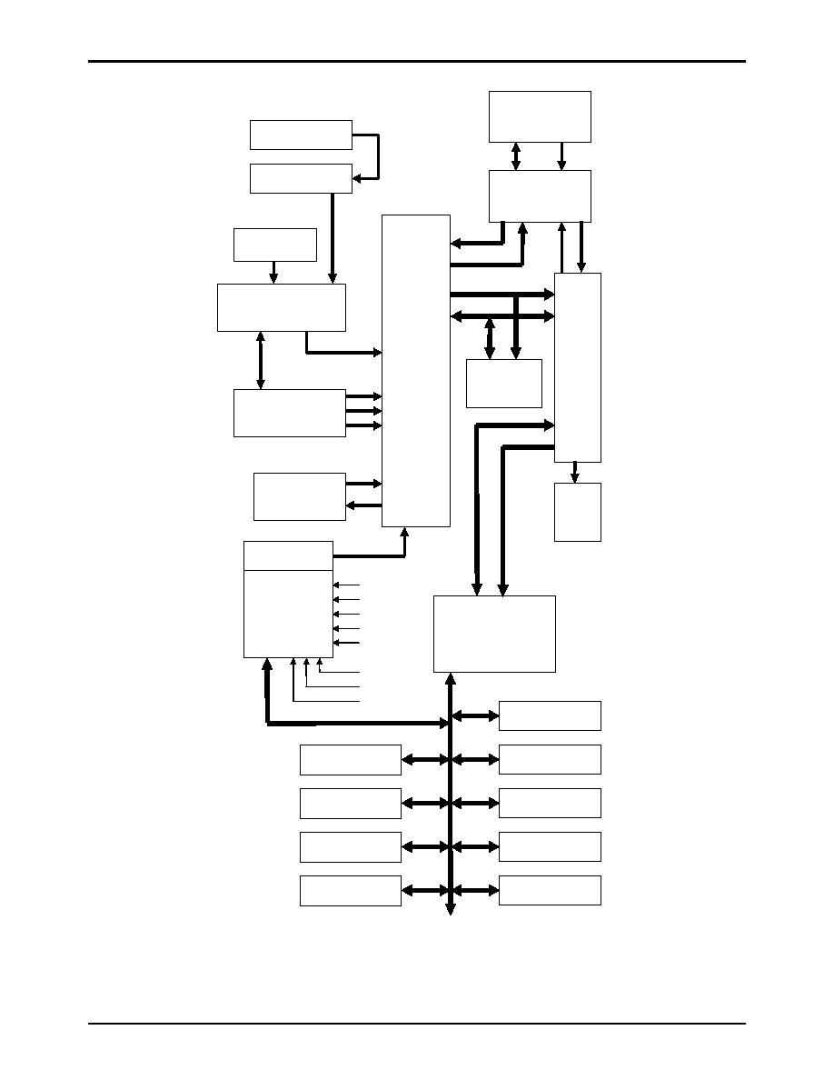
System Block Diagram
32bit
RISC
CORE
Special Function Register
SFR Bus Control
DRAM
Control
Data RAM
(2k bytes)
Instruction Cache
(2k bytes)
Interrupt enable
control
Coprocessor
(Multiplier)
Mode Control
Reset Control
RC OSC
Multiplier Circuit
Main OSC
System Clock, Standby
Control
Interrupt Control
Timer 0
Timer 1
Timer 2
Timer 3
SIO0
UART0
UART1
Port 0
Port 1
Instruction Cache
Control
Bus
Control
SIO0
UART0
UART1
TM0H
TM0L
TM1H
TM2H
TM3H
Figure 1 LC680100A System Block Diagram
LC680100A
No.6830-3/16
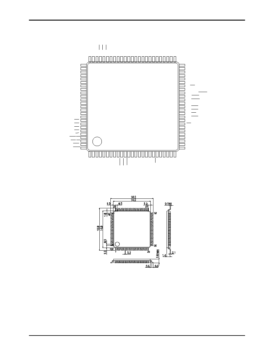
Terminal Assignment Diagram
(SQFP100, 0.5mm pitch)
1 2 3 4 5 6 7 8 9 10 11 12 13 14 15 16 17 18 19 20 21 22 23 24 25
26
27
28
29
30
31
32
33
34
35
36
37
38
39
40
41
42
44
45
46
47
48
49
50
43
57 56 55 54 53 52 51
60 59 58
67 66 65 64 63 62
70 69 68
61
75 74 73 72 71
84
83
82
81
80
78
77
76
79
85
94
93
92
91
90
88
87
86
89
95
100
98
97
96
99
VD
D
CK
1
CK
2
VS
S
CM
P
VD
D
CK
O
T
CK
IN
VS
S
PH
I
O
T
HO
L
D
I
R
ESET
MO
D
E
TE
S
T
VD
D
P0
0
/
T
X
D
0
P
0
1
/
RX
D0
P0
2
/
S
D
O
P0
3
/
S
D
I
P0
4
/
S
C
K
P0
5
/
P
W
M
0
P0
6
/
P
W
M
1
P0
7
/
T
0
I
N
/
I
N
T
0
VS
S
P0
8
/
I
N
T
1
P09/INT2
P0A/INT3
P0B/PWM2
P0C/TXD1
P0D/RXD1
P0E
P0F
NMI
P10/BGNT
P11/RAS
P12/CASU
P13/CASL
P14/DMXS
P15/RFREQ
P16/IRQOT
P17/MCLK/HOLDO
VDD
A1
A2
A3
A4
A5
A6
VSS
A0/LBS
A7
A8
A9
A1
0
VD
D
A1
1
A1
2
A1
3
A1
4
A1
5
A1
6
A1
7
A1
8
A1
9
A2
0
A2
1
A2
2
A2
3
A2
4
A2
5
/
C
S
5
A2
6
/
C
S
4
A2
7
/
C
S
3
VS
S
D0
D1
D2
D3
D4
D5
D6
D7
VDD
D8
D9
D10
D11
D12
D13
D14
D15
VSS
CS0
CS1
CS2
CS6
RD
WRU/UBS
WRL/WR
WAIT
BREQ
LC680100A
Package Dimension
(unit : mm)
3181B
SANYO : SQFP-100
LC680100A
No.6830-4/16
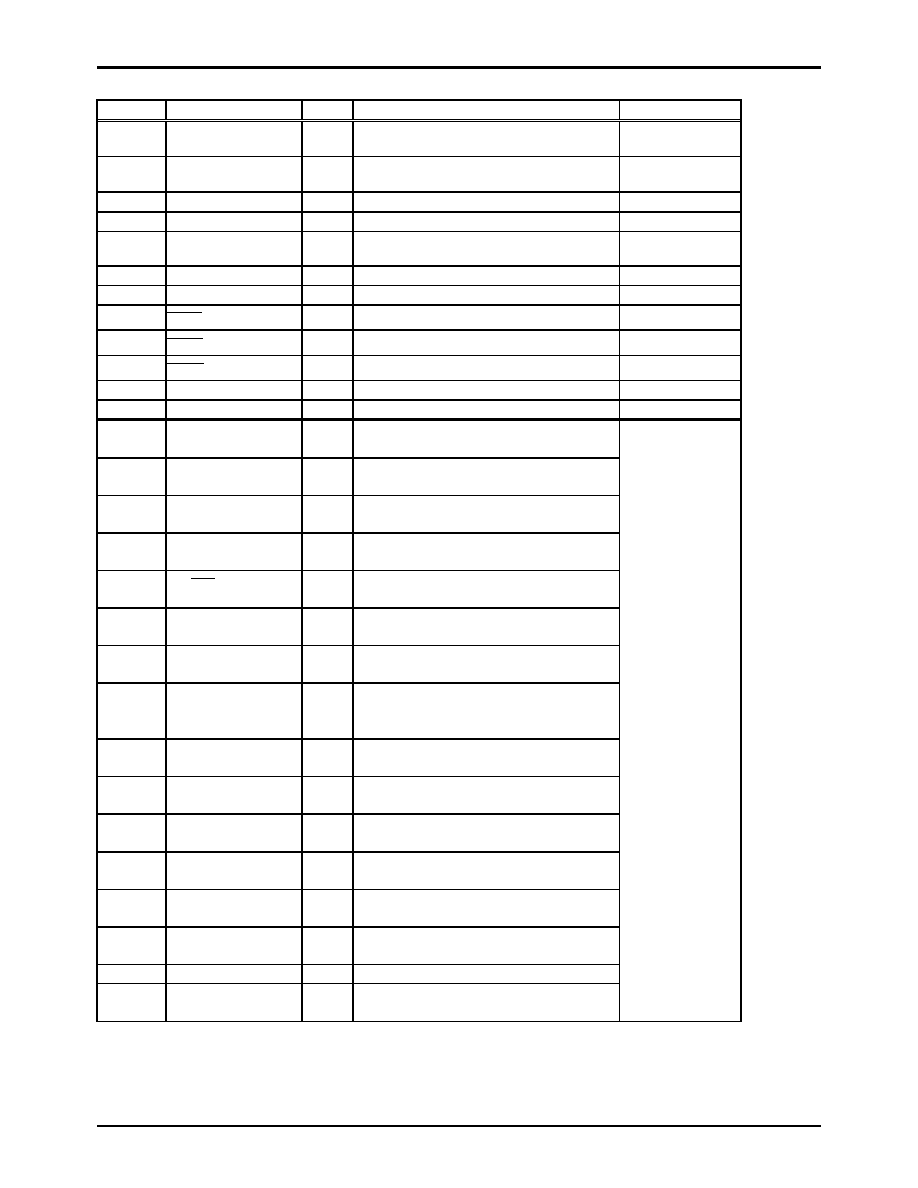
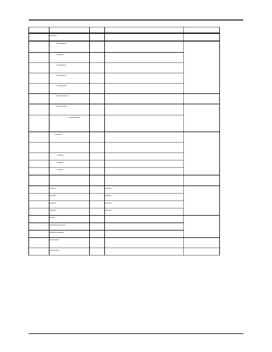
Terminal Functions
Note: PU = pull-up
Pin Number
Pin Name
I/O
Function Description
Pin Format
1,6,15,34,55
,82
VDD
-
Power supply +ve
-
4,9,24,43,73
,91
VSS -
Power
supply
-ve
-
2
CK1
I
Input to main oscillator
Schmitt Input
3
CK2
O
Output from main oscillator
CMOS output
5
CMP
I/O
Phase comparator filter pin (multiplier circuit).
Schmitt Input∑Tristate
output
7
CKOT
O
CK1 or half frequency clock output from multiplier CMOS output
8
CKIN
I
External clock input
Schmitt Input
10
PHIOT
O
System clock output
CMOS output
11
HOLDI
I
HOLD request input
Schmitt Input
12
RESET
I
Reset terminal
Schmitt Input
13
MODE
I
Bus mode setting at reset
Schmitt Input
14
TEST
I
Test input (Normally connected to VSS)
Schmitt Input
16
P00/TXD0
I/O
PORT0 bit0 I/O.
Also UART0 send
17
P01/RXD0
I/O
PORT0 bit1 I/O.
Also UART0 receive
18
P02/SDO
I/O
PORT0 bit2 I/O.
Also SIO0 data out
19
P03/SDI
I/O
PORT0 bit3 I/O.
Also SIO0 data in
20
P04/
SCK
I/O
PORT0 bit4 I/O.
Also SIO0 clock
21
P05/PWM0
I/O
PORT0 bit5 I/O.
Also PWM0 output
22
P06/PWM1
I/O
PORT0 bit6 I/O.
Also PWM1 output
23
P07/T0IN/INT0
I/O
PORT0 bit7 I/O.
Timer0 event input
INT0 input
25
P08/INT1
I/O
PORT0 bit8 I/O.
INT1 input
26
P09/INT2
I/O
PORT0 bit9 I/O.
INT2 input
27
P0A/INT3
I/O
PORT0 bit10 I/O.
INT3 input
28
P0B/PWM2
I/O
PORT0 bit11 I/O.
PWM2 output
29
P0C/TXD1
I/O
PORT0 bit12 I/O.
UART1 send
30
P0D/RXD1
I/O
PORT0 bit13 I/O.
UART1 receive
31
P0E
I/O
PORT0 bit14 I/O.
32
P0F
I/O
PORT0 bit15 I/O.
∑Used as input:
Schmitt Input;
presence of PU
resistor software
selectable.
∑Used as Output:
CMOS/N-ch OD
mode software
selectable.
LC680100A
No.6830-5/16
Pin Number
Pin Name
I/O
Function Description
Pin Format
33
NMI
I
NMI interrupt
Schmitt Input
35
P10/
BGNT
I/O
PORT1 bit0 input.
Also bus grant output.
36
P11/
RAS
I/O
PORT1 bit1 input. Also
DRAM control RAS signal out.
37
P12/
CASU
I/O
PORT1 bit2 input. Also
DRAM control CASU signal out.
38
P13/
CASL
I/O
PORT1 bit3 input. Also
DRAM control CASL signal out.
39
P14/
DMXS
I/O
PORT1 bit4 input. Also
DRAM control DMXS signal out.
Schmitt Input∑Tristate
output
40
P15/
RFREQ
I/O
PORT1 bit5 input. Also
DRAM control RFREQ I/O.
Schmitt Input∑PU
Output
41
P16/
IRQOT
I/O
PORT1 bit6 input.
Also IRQOT output.
42
P17/MCLK/
HOLD0
I/O
PORT1 bit7 input.
MCLK output,
HOLD state output
Schmitt Input∑Tristate
output
44
A0/
LBS
I/O
Bus Address bit0 or
Lower byte strobe signal.
45 to 54,
56 to 69
A1to A24
I/O
Bus Address bit1 to 24.
70
A25/
CS5
I/O
Bus Address bit25 or CS5.
71
A26/
CS4
I/O
Bus Address bit26 or CS4
72
A27/
CS3
I/O
Bus Address bit27 or CS3.
Schmitt Input∑Tristate
output
74 to 81,
83 to 90
D0 to D15
I/O
Bus data bit0 to 15
Schmitt Input∑Tristate
output
92
CS0
I/O
CS0
93
CS1
I/O
CS1
94
CS2
I/O
CS2
95
CS6
I/O
CS6
Schmitt Input∑Tristate
output
96
RD
I/O
Bus read signal.
97
WRU
/
UBS
I/O Upper byte write signal or Upper byte strobe.
98
WRL
/
WR
I/O Upper byte write signal or Write.
Schmitt Input∑Tristate
output
99
WAIT
I/O
Bus cycle wait
Schmitt Input∑PU
output
100
BREQ
I
Bus request.
Schmitt Input