 | –≠–ª–µ–∫—Ç—Ä–æ–Ω–Ω—ã–π –∫–æ–º–ø–æ–Ω–µ–Ω—Ç: LC7150 | –°–∫–∞—á–∞—Ç—å:  PDF PDF  ZIP ZIP |
FCC 10-Channel Standard PLL For Cordless
Telephone
Functions
.
On-chip PLL for transmission/reception
.
On-chip digital unlock detector (only PLL for transmission)
.
5.0 kHz/4.4 kHz output pins for guard tone
.
Standby function
.
Pull-down resistance at channel select pins (D1 to D4)
LC7150: With (for mechanical switch)
LC7151: Without (for microcontroller)
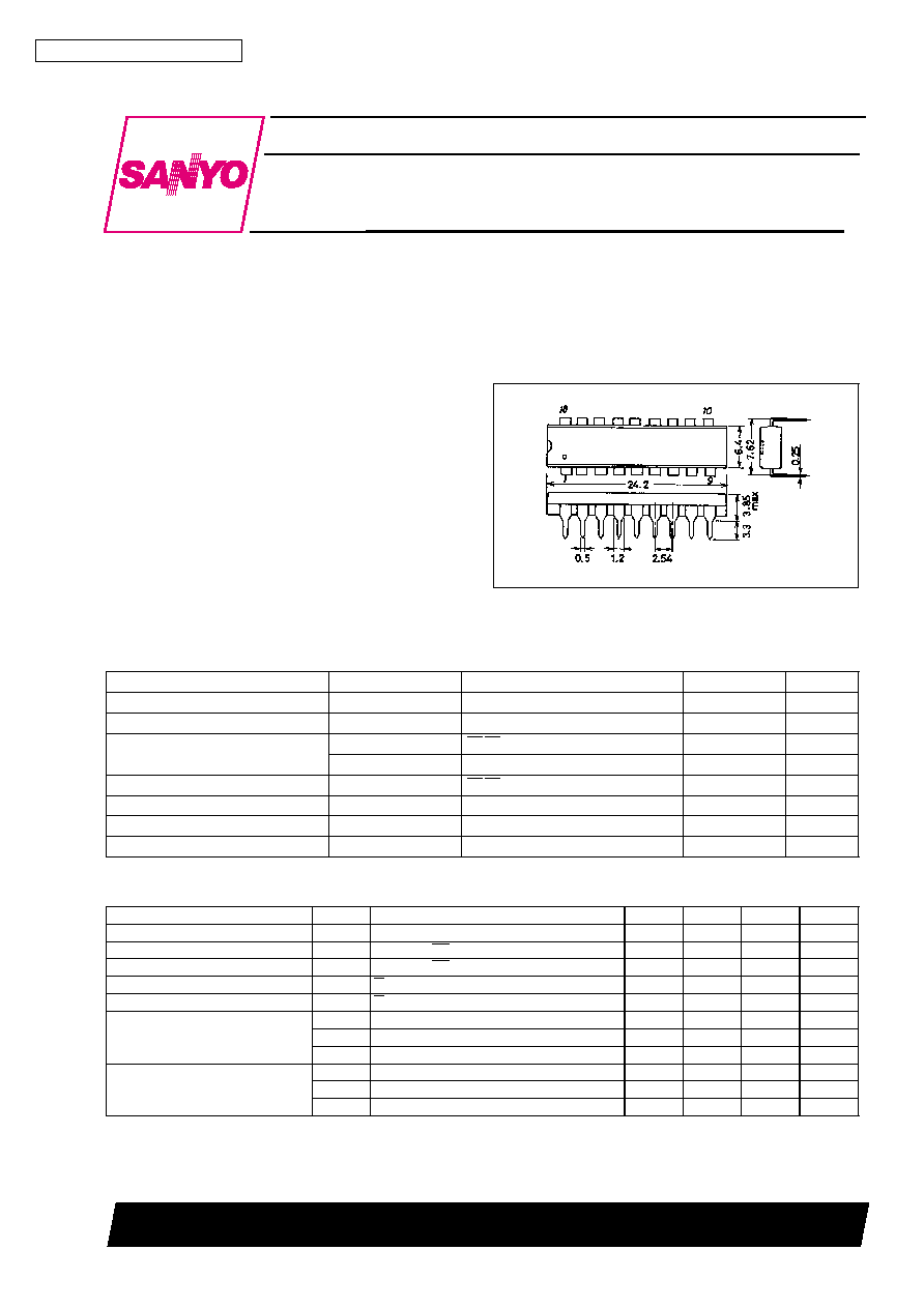
Package Dimensions
unit : mm
3007A-DIP18
[LC7150]
SANYO : DIP18
Specifications
Absolute Maximum Ratings
at Ta = 25∞C, V
SS
= 0 V
Parameter
Symbol
Conditions
Ratings
Unit
Maximum supply voltage
V
DD
max
≠0.3 to +6.5
V
Maximum input voltage
V
I
max
All input pins
≠0.3 to V
DD
+0.3
V
Maximum output voltage
V
O
1 max
F1,F2 Output OFF
≠0.3 to +6.5
V
V
O
2 max
Output pins other than V
O
1
≠0.3 to V
DD
+0.3
V
Output current
I
OUT
F1,F2, LDT
0 to 3.0
mA
Allowable power dissipation
Pd max
Ta
%
75∞C
350
mW
Operating temperature
Topr
≠30 to +75
∞C
Storage temperature
Tstg
≠40 to +125
∞C
Allowable Operating Conditions
at Ta = 25∞C, V
SS
= 0 V
Parameter
Symbol
Conditions
min
typ
max
Unit
Supply voltage
V
DD
3.0
5.5
V
Input high-level voltage
V
IH
1
D1 to D4, SB
0.7 V
DD
V
DD
V
Input low-level voltage
V
IL
1
D1 to D4, SB
0
0.3V
DD
V
Input high-level voltage
V
IH
2
R/B
0.9 V
DD
V
DD
V
Input low-level voltage
V
IL
2
R/B
0
0.1V
DD
V
Input frequency
f
IN
1
PIT; V
IN
= 0.15 Vrms
10
27
MHz
f
IN
2
PIR; V
IN
= 0.15 Vrms
30
42
MHz
f
IN
3
XIN; V
IN
= 0.3 Vrms
5.0
10.24
11.0
MHz
Input amplitude
V
IN
1
PIT; f
IN
= 27 MHz
0.15
0.3V
DD
Vrms
V
IN
2
PIR; f
IN
= 42 MHz
0.15
0.3V
DD
Vrms
V
IN
3
XIN; f
IN
= 11 MHz
0.3
0.3V
DD
Vrms
Ordering number: EN1634G
CMOS LSI
LC7150
SANYO Electric Co.,Ltd. Semiconductor Bussiness Headquarters
TOKYO OFFICE Tokyo Bldg., 1-10, 1 Chome, Ueno, Taito-ku, TOKYO, 110 JAPAN
O3096HA(II)/11393JN/6297TA/7245KI/7104KI,TS No.1634-1/5
Electrical Characteristics
at Ta = 25∞C, under Allowable Operating Conditions
Parameter
Symbol
Conditions
min
typ
max
Unit
Input high-level current
I
IH
1
XIN; V
I
= V
DD
20
µA
Input low-level current
I
IL
1
XIN; V
I
= V
SS
20
µA
Input high-level current
I
IH
2
PIT, PIR; V
I
= V
DD
40
µA
Input low-level current
I
IL
2
PIT, PIR; V
I
= V
SS
40
µA
Input high-level current
I
IH
3
SB,R/B; V
I
= V
DD
10
µA
Input low-level current
I
IL
3
SB, R/B; V
I
= V
SS
10
µA
Input pull-down resistance
Rd
D1 to D4
10
20
40
k
Input floating voltage
V
IF
D1 to D4; Open
0.1V
DD
V
Feedback resistance
Rf1
XIN; V
DD
= 4.3 V
1.0
M
Rf2
PIT, PIR; V
DD
= 4.3 V
0.5
M
Output high-level voltage
V
OH
1
PDT, PDR; I
O
= 0.5mA
V
DD
≠1.0
V
Output low-level voltage
V
OL
1
PDT, PDR; V
O
= 0.5 mA
1.0
V
Output OFF leak current
Ioff1
PDT,PDR; V
O
= V
DD
/V
SS
0.01
1.0
nA
Output high-level voltage
V
OH
2
LDT; I
O
= 1 mA
V
DD
≠1.0
V
Output OFF leak current
Ioff2
LDT; Output OFF V
O
= V
SS
5.0
µA
Output low-level voltage
V
OL
2
F1,F2; I
O
= 1 mA
1.0
V
Output OFF leak current
Ioff3
F1,F2; Output OFF V
O
= 5.5 V
5.0
µA
Supply current
I
DD
1
(C3) V
DD
= 3.0 V
4
mA
I
DD
2
(C3) V
DD
= 4.5 V
7
mA
I
DD
3
(C3) V
DD
= 5.5 V
13
mA
I
DD
4
(C2) V
DD
= 3.0 V
3
mA
I
DD
5
(C2) V
DD
= 4.5 V
5
mA
I
DD
6
(C2) V
DD
= 5.5 V
10
mA
(C3): XIN = 10.24 MHz, xtal connected
PIT = 27 MHz 150 mVrms
PIR = 42 MHz 150 mVrms
R/B= V
DD
, SB = V
DD
, Other pin open
(C2): XIN = 10.24 MHz, xtal connected
PIR = 42 MHz, 150 mVrms
R/B= V
DD
, SB = V
SS
, Other pin open
(Note) Power supply V
DD
≠ V
SS
: Insert a capacitor of 2000 pF or greater.
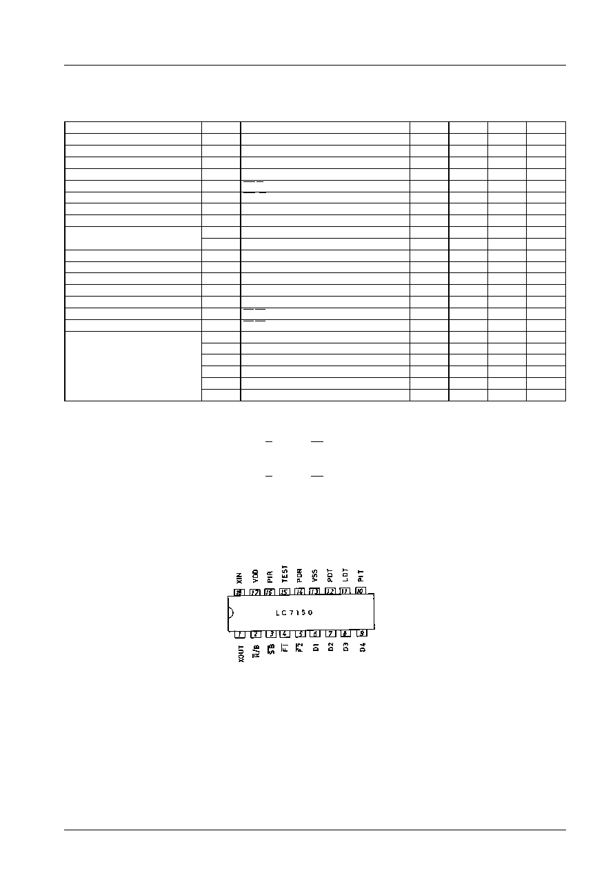
Pin Assignment
Top view
LC7150
No.1634-2/5
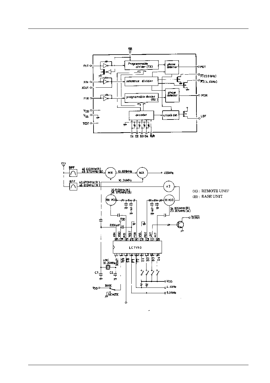
Equivalent Circuit Block Diagram
Sample Application Circuit
Crystal resonator: HC43/U
2114-85501: CL = 10 pF
C1 = 15 (10 to 22) pF C2 = 15 pF
2114-85502: CL = 16 pF
C1 = 22 (15 to 33) pF C2 = 33 pF
KINSEKI, LTD.
Each value (Hz) is for 1
channel.
V
DD
: TX, RX and PLL are operated.
V
SS
: Only RX and PLL are operated.
When 5.0 kHz/4.4 kHz pins are not used,
connect these pins to V
SS
.
LC7150
No.1634-3/5
Pin Description
Pin
Description
F1
5.0 kHz output. When not used, connect to V
SS
.
F2
4.4 kHz output (10.24 MHz
˜
2304). When not used, connect to V
SS
.
V
DD
, V
SS
Power supply.
XIN, XOUT
Crystal resonator (10.24 MHz).
D1 to D4
Channel select pin.
R/B
Base unit/remote unit select pin.
R/B = ``0'' (V
SS
) ...... Remote unit
R/B = ``1'' (V
DD
) ...... Base unit
SB
Used to stop the TX PLL at the standby mode to minimize current dissipation.
SB = ``0'' (V
SS
) ...... Standby mode. Only the RX and PLL are operated. The charge pump enters a
high-impedance mode.
SB = ``1'' (V
DD
) ...... The TX, RX and PLL are operated.
PIT
TX programmable divider input pin.
PIR
RX programmable divider input pin.
PDT
TX charge pump output pin.
PDR
RX charge pump output pin.
TEST
LSI test input pin. Connected to V
SS.
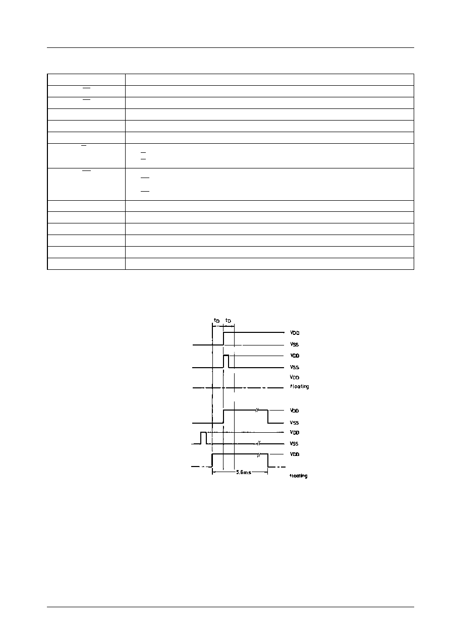
LDT
TX PLL unlock signal output pin.
When the phase difference becomes t
D
(= 6.25 µs.) or more, 5.6 ms. output pulse is delivered at the LDT pin.
Reference divider
Programmable divider
LDT
Reference divider
Programmable divider
LDT
LC7150
No.1634-4/5
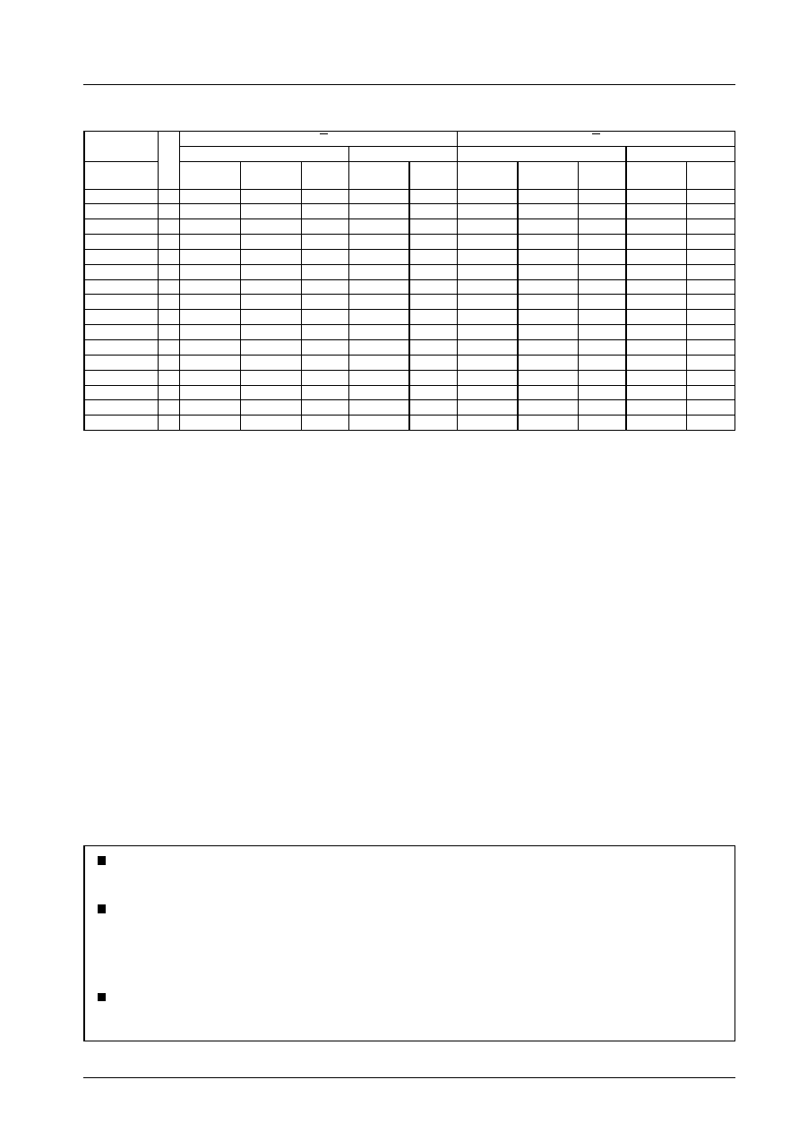
Table of Frequency Division
INPUT
C
H
REMOTE (R/B = ``0'')
BASE (R/B=``1'')
TX (fref = 2.5 kHz)
RX (fref = 5 kHz)
TX (fref = 2.5 kHz)
RX (fref = 5 kHz)
D1 D2 D3 D4
f
TX
(MHz)
f
VCO
(MHz)
N
f
VCO
(MHz)
N
f
TX
(MHz)
f
VCO
(MHz)
N
f
VCO
(MHz)
N
1 0 0 0
1
49.670
24.8350
9934
35.915
7183
46.610
23.305
9322
38.975
7795
0 1 0 0
2
49.845
24.9225
9969
35.935
7187
46.630
23.315
9326
39.150
7830
1 1 0 0
3
49.860
24.9300
9972
35.975
7195
46.670
23.335
9334
39.165
7833
0 0 1 0
4
49.770
24.8850
9954
36.015
7203
46.710
23.355
9342
39.075
7815
1 0 1 0
5
49.875
24.9375
9975
36.035
7207
46.730
23.365
9346
39.180
7836
0 1 1 0
6
49.830
24.9150
9966
36.075
7215
46.770
23.385
9354
39.135
7827
1 1 1 0
7
49.890
24.9450
9978
36.135
7227
46.830
23.415
9366
39.195
7839
0 0 0 1
8
49.930
24.9650
9986
36.175
7235
46.870
23.435
9374
39.235
7847
1 0 0 1
9
49.990
24.9950
9998
36.235
7247
46.930
23.465
9386
39.295
7859
0 1 0 1
10
49.970
24.9850
9994
36.275
7255
46.970
23.485
9394
39.275
7855
1 1 0 1
10
49.970
23.9850
9994
36.275
7255
46.970
23.485
9394
39.275
7855
0 0 1 1
10
49.970
23.9850
9994
36.275
7255
46.970
23.485
9394
39.275
7855
1 0 1 1
10
49.970
23.9850
9994
36.275
7255
46.970
23.485
9394
39.275
7855
0 1 1 1
10
49.970
23.9850
9994
36.275
7255
46.970
23.485
9394
39.275
7855
1 1 1 1
10
49.970
23.9850
9994
36.275
7255
46.970
23.485
9394
39.275
7855
0 0 0 0
10
49.970
23.9850
9994
36.275
7255
46.970
23.485
9394
39.275
7855
No products described or contained herein are intended for use in surgical implants, life-support systems, aerospace equipment,
nuclear power control systems, vehicles, disaster/crime-prevention equipment and the like, the failure of which may directly or
indirectly cause injury, death or property loss.
Anyone purchasing any products described or contained herein for an above-mentioned use shall:
1
Accept full responsibility and indemnify and defend SANYO ELECTRIC CO., LTD., its affiliates, subsidiaries and distributors
and all their officers and employees, jointly and severally, against any and all claims and litigation and all damages, cost and
expenses associated with such use:
2
Not impose any responsibility for any fault or negligence which may be cited in any such claim or litigation on SANYO
ELECTRIC CO., LTD., its affiliates, subsidiaries and distributors or any of their officers and employees jointly or severally.
Information (including circuit diagrams and circuit parameters) herein is for example only; it is not guaranteed for volume
production. SANYO believes information herein is accurate and reliable, but no guarantees are made or implied regarding its use
or any infringements of intellectual property rights or other rights of third parties.
This catalog provides information as of October, 1996. Specifications and information herein are subject to change without notice.
LC7150
No.1634-5/5