 | –≠–ª–µ–∫—Ç—Ä–æ–Ω–Ω—ã–π –∫–æ–º–ø–æ–Ω–µ–Ω—Ç: LC72122V | –°–∫–∞—á–∞—Ç—å:  PDF PDF  ZIP ZIP |
CMOS IC
Ordering number : ENN6113A
D0199TH (OT) /O3099TH (OT) /D2598RM (OT) No. 6113-1/22
SANYO Electric Co.,Ltd. Semiconductor Company
TOKYO OFFICE Tokyo Bldg., 1-10, 1 Chome, Ueno, Taito-ku, TOKYO, 110-8534 JAPAN
PLL Frequency Synthesizer
for Portable Equipment Electronic Tuning
LC72122V
Overview
The LC72122V is a low-voltage (1.8 to 3.6 V) PLL
frequency synthesizer IC that allows portable TV
(VHF)/FM/AM tuners to be constructed easily.
Features
∑ High-speed programmable frequency divider
-- FMIN: 10 to 250 MHz ..Pulse swallower
(divide-by-two prescaler built in)
-- AMIN: 2 to 40 MHz ......Pulse swallower
0.5 to 10 MHz ...Direct division
∑ IF counter
-- IFIN: 0.4 to 12 MHz ......For use as an AM/FM IF
counter
∑ Reference frequency
-- Selectable from one of nine frequencies (crystal
oscillator: 75 kHz)
1, 2.5, 3, 5, 3.125, 6.25, 12.5, 15, and 25 kHz
∑ Phase comparator
-- Supports dead zone control
-- Built-in unlock detection circuit
-- Built-in deadlock clear circuit
-- Sub-charge pump for fast frequency locking
∑ Built-in MOS transistor for forming an active low-pass
filter
∑ I/O ports
-- Dedicated output ports: 3
-- I/O ports: 2
-- Supports clock time base output
∑ Serial Data I/O
-- Supports CCB format communication with the
system controller.
∑ Operating ranges
-- Supply voltage: 1.8 to 3.6 V
-- Operating temperature: ≠20 to +70∞C
∑ Package
--SSOP20
Package Dimensions
unit: mm
3179A-SSOP20
Any and all SANYO products described or contained herein do not have specifications that can handle
applications that require extremely high levels of reliability, such as life-support systems, aircraft's
control systems, or other applications whose failure can be reasonably expected to result in serious
physical and/or material damage. Consult with your SANYO representative nearest you before using
any SANYO products described or contained herein in such applications.
SANYO assumes no responsibility for equipment failures that result from using products at values that
exceed, even momentarily, rated values (such as maximum ratings, operating condition ranges, or other
parameters) listed in products specifications of any and all SANYO products described or contained
herein.
∑ CCB is a trademark of SANYO ELECTRIC CO., LTD.
∑ CCB is SANYO's original bus format and all the bus
addresses are controlled by SANYO.
1
10
11
6.4
6.7
0.5
4.4
0.1
1.6max
1.0
20
0.65
0.22
0.43
0.15
SANYO: SSOP20
[LC72122V]
No. 6113-2/22
LC72122V
Specifications
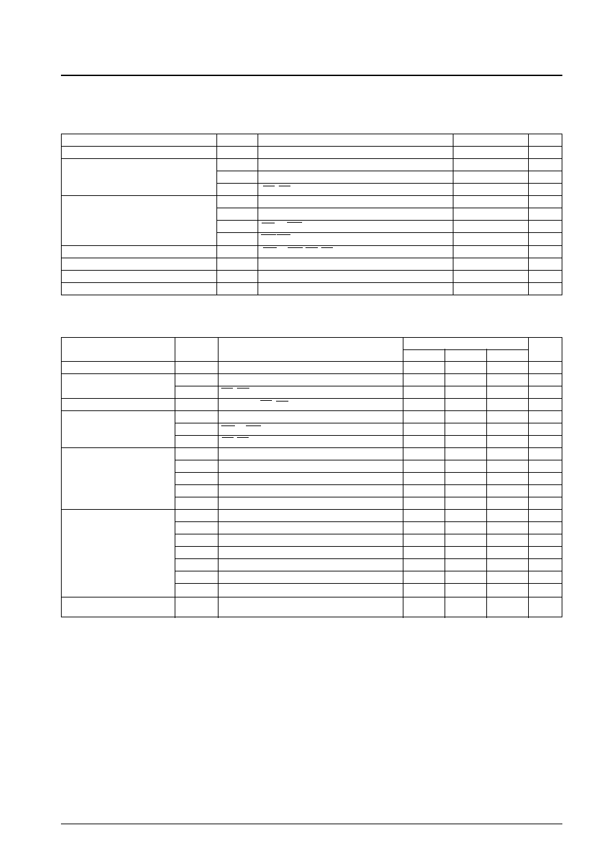
Absolute Maximum Ratings
at Ta = 25∞C, V
SSd
= V
SSa =
0 V
Parameter
Symbol
Conditions
Ratings
Unit
Maximum supply voltage
V
DD
max
V
DD
≠0.3 to +4.0
V
V
IN
1 max
CE, CL, DI
≠0.3 to +7.0
V
Maximum input voltage
V
IN
2 max
XIN, FMIN, AMIN, IFIN, AIN
≠0.3 to V
DD
+ 0.3
V
V
IN
3 max
IO1, IO2
≠0.3 to +8
V
V
O
1 max
DO
≠0.3 to +7.0
V
Maximum output voltage
V
O
2 max
XOUT, PD
≠0.3 to V
DD
+ 0.3
V
V
O
3 max
BO1 to BO3,AOUT
≠0.3 to +15
V
V
O
4 max
IO1, IO2
≠0.3 to +8
V
Maximum output current
I
O
max
BO1 to BO3, IO1, IO2, DO, AOUT
0 to 6.0
mA
Allowable power dissipation
Pd max
Ta
70∞C: SSOP20
150
mW
Operating temperature
Topr
≠20 to +70
∞C
Storage temperature
Tstg
≠40 to +125
∞C
Ratings
Parameter
Symbol
Conditions
min
typ
max
Unit
Supply voltage
V
DD
V
DD
1.8
2.2
3.6
V
Input high-level voltage
V
IH
1
CE, CL, DI
0.7 V
DD
6.5
V
V
IH
2
IO1, IO2
0.7 V
DD
7
V
Input low-level voltage
V
IL
CE, CL, DI, IO1, IO2
0
0.3 V
DD
V
V
O
1
DO
0
6.5
V
Output voltage
V
O
2
BO1 to BO3, AOUT
0
13
V
V
O
3
IO1, IO2
0
7
V
f
IN
1
XIN: V
IN
1
75
kHz
f
IN
2
FMIN: V
IN
2
10
250
MHz
Input frequency
f
IN
3
AMIN: V
IN
3, SNS = 1
2
40
MHz
f
IN
4
AMIN: V
IN
4, SNS = 0
0.5
10
MHz
f
IN
5
IFIN: V
IN
5
0.4
12
MHz
V
IN
1
XIN: f
IN
1
200
600
mVrms
V
IN
2-1
FMIN: f = 10 to 50 MHz
50
600
mVrms
V
IN
2-2
FMIN: f = 50 to 250 MHz
40
600
mVrms
Input amplitude
V
IN
3
AMIN: f
IN
3, SNS = 1
30
600
mVrms
V
IN
4
AMIN: f
IN
4, SNS = 0
30
600
mVrms
V
IN
5-1
IFIN: f
IN
5, IFS = 1
30
600
mVrms
V
IN
5-2
IFIN: f
IN
5, IFS = 0
70
600
mVrms
Guaranteed crystal
Xtal
XIN, XOUT
*
75
kHz
oscillator frequency
Allowable Operating Ranges
at Ta = ≠20 to +70∞C, V
SSd
= V
SSa =
0 V
*
Note : Recommended crystal oscillator CI value : CI
35 k
(for a 75kHz crystal )
The circuit constants for the crystal oscillator circuit depend on the crystal used, the printed sircuit board pattem, and other items. Therefore we
recommend consulting with the manfacturer of the crystal for evaluation and reliability.
The extremely high input impedance of the XIN pins means that applications must take the possibility of leakage into account.

No. 6113-3/22
LC72122V
Electrical Characteristics
within the allowable operating ranges
Ratings
Parameter
Symbol
Conditions
min
typ
max
Unit
Rf1
XIN
8.0
M
Internal feedback resistors
Rf2
FMIN
500
k
Rf3
AMIN
500
k
Rf4
IFIN
500
k
Internal pull-down resistors
Rpd1
FMIN
200
k
Rpd2
AMIN
200
k
Internal output resistor
Rd
XOUT
250
k
Hysteresis
V
HIS
CE, CL, DI, IO1, IO2
0.1 V
DD
V
V
OH
1
PD: I
O
= ≠1 mA
V
DD
≠ 0.5
V
Output high-level voltage
V
OH
2
AIN (PDS) : I
O
= ≠ 2 mA (V
DD
= 1.8 to 2.7 V)
V
DD
≠ 0.5
V
AIN (PDS) : I
O
= ≠ 4 mA (V
DD
= 2.7 to 3.6 V)
V
DD
≠ 0.5
V
V
OL
1
PD: I
O
= 1 mA
0.5
V
V
OL
2
AIN (PDS) : I
O
= 2 mA (V
DD
= 1.8 to 2.7 V)
0.5
V
AIN (PDS) : I
O
= 4 mA (V
DD
= 2.7 to 3.6 V)
0.5
V
BO1 to BO3, IO1, IO2; I
O
= 1 mA
0.2
V
Output low-level voltage
V
OL
3
BO1 to BO3, IO1, IO2; I
O
= 5 mA
1.0
V
BO1 to BO3, IO1, IO2; I
O
= 8 mA
1.6
V
V
OL
4
DO: I
O
= 1 mA
0.2
V
DO: I
O
= 5 mA
1.0
V
V
OL
5
AOUT, I
O
= 5 mA, A
IN
= 1.2 V
1.5
V
I
IH
1
CE, CL, DI: V
I
= 6.5 V
5.0
µA
I
IH
2
IO1, IO2: V
I
= 7 V
5.0
µA
Input high-level current
I
IH
3
XIN: V
I
= V
DD
0.11
0.45
1.3
µA
I
IH
4
FMIN, AMIN: V
I
= V
DD
1.8
7.2
22
µA
I
IH
5
IFIN: V
I
= V
DD
1.8
7.2
22
µA
I
IH
6
AIN: V
I
= V
DD
200
nA
I
IL
1
CE, CL, DI: V
I
= 0 V
5.0
µA
I
IL
2
IO1, IO2: V
I
= 0 V
5.0
µA
Input low-level current
I
IL
3
XIN: V
I
= 0 V
0.11
0.45
1.3
µA
I
IL
4
FMIN, AMIN: V
I
= 0 V
1.8
7.2
22
µA
I
IL
5
IFIN: V
I
= 0 V
1.8
7.2
22
µA
I
IL
6
AIN: V
I
= 0 V
200
nA
I
OFF
1
BO1 to BO3, AOUT: V
O
= 13 V
5.0
µA
Output off leakage current
I
OFF
2
IO1, IO2: V
O
= 7 V
5.0
µA
I
OFF
3
DO: V
O
= 6.5 V
5.0
µA
High-level three-state off
I
OFFH
PD: V
O
= V
DD
0.01
200
nA
leakage current
Low-level three-state off
I
OFFL
PD: V
O
= 0 V
0.01
200
nA
leakage current
Input capacitance
C
IN
FMIN
6
pF
I
DD
1
V
DD
: Xtal = 75 kHz, f
IN
2 = 250 MHz, V
IN
2 = 40 mVrms
4
10
mA
Supply current
I
DD
2
V
DD
: PLL block stopped (PLL inhibit),
10
µA
Xtal oscillator operating (Xtal = 75 kHz)
I
DD
3
V
DD
: PLL block stopped, Xtal oscillator stopped
10
µA
No. 6113-4/22
LC72122V
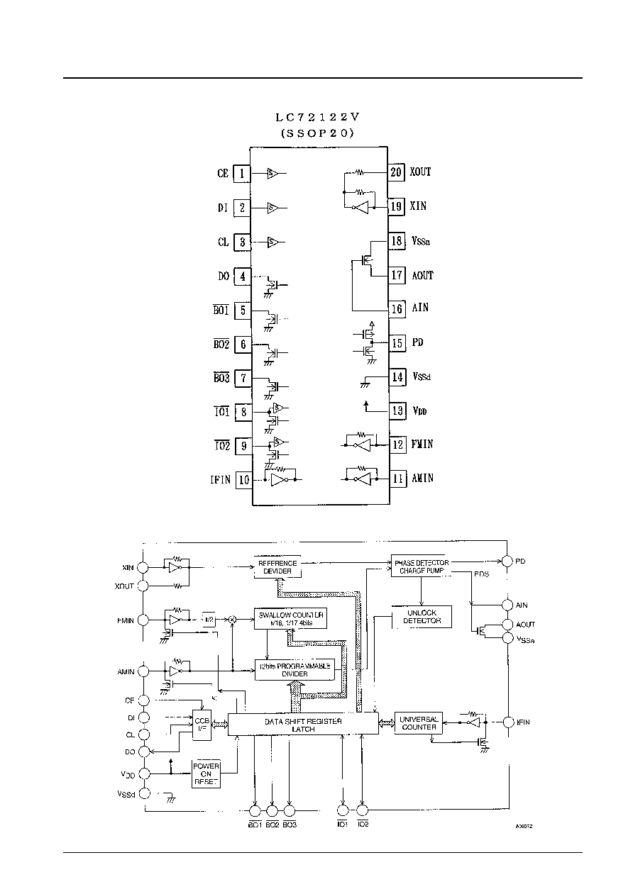
Pin Assignment
Top view
Block Diagram
No. 6113-5/22
LC72122V
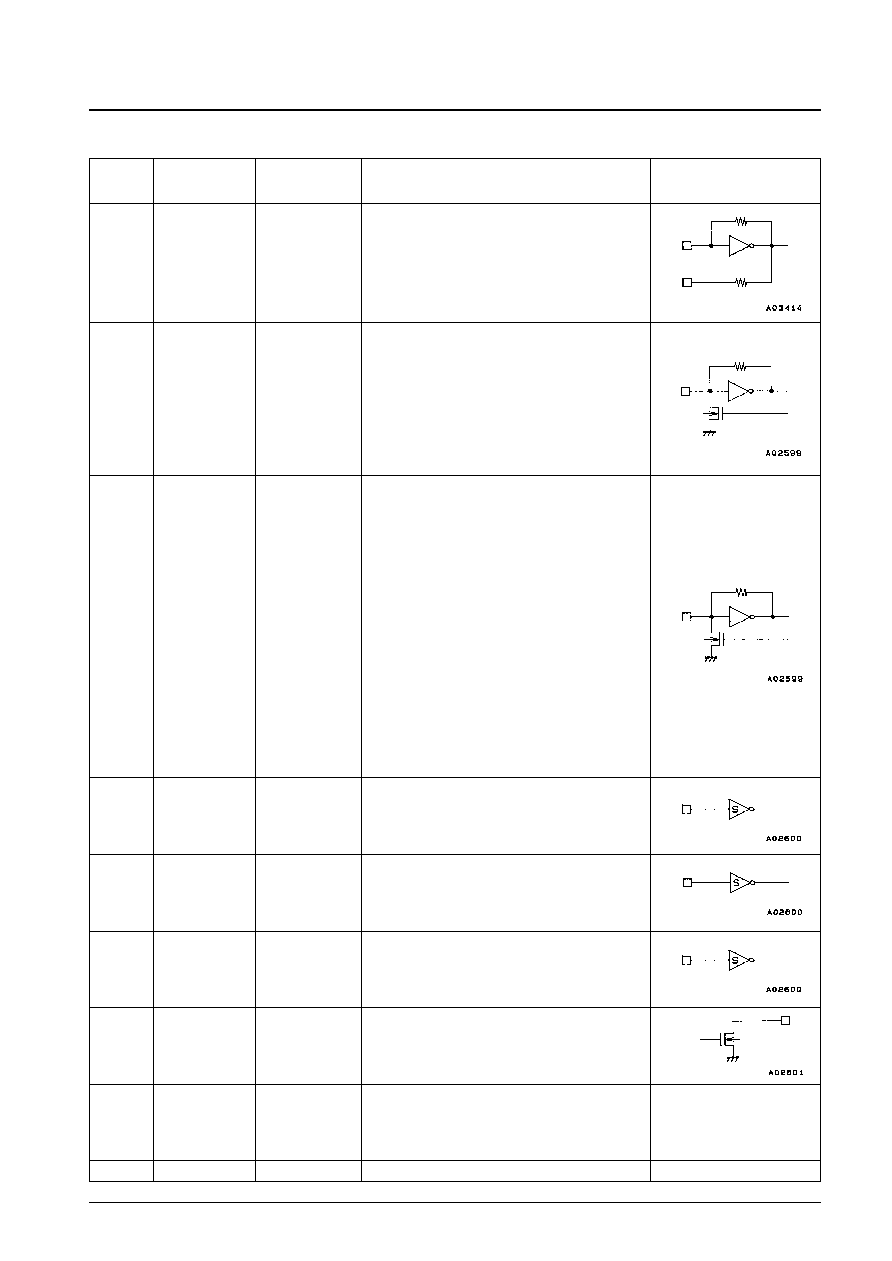
Pin Descriptions
Symbol
Pin No.
Type
Functions
Circuit configuration
19
20
12
11
1
3
2
4
13
14
XIN
XOUT
FMIN
AMIN
CE
CL
DI
DO
V
DD
V
SSd
Xtal
Local oscillator
signal input
Local oscillator
signal input
Chip enable
Clock
Input data
Output data
Power supply
Ground
∑ Crystal oscillator connections (75 kHz)
∑ FMIN is selected when the serial data input DVS bit is
set to 1.
∑ The input frequency range is from 10 to 250 MHz.
∑ The input signal passes through the internal divide-by-
two prescaler and is input to the swallow counter.
∑ The divisor can be in the range 272 to 65535. However,
since the signal has passed through the divide-by-two
prescaler, the actual divisor is twice the set value.
∑ AMIN is selected when the serial data input DVS bit is
set to 0.
∑ When the serial data input SNS bit is set to 1:
-- The input frequency range is 2 to 40 MHz.
-- The signal is directly input to the swallow counter.
-- The divisor can be in the range 272 to 65535, and
the divisor used will be the value set.
∑ When the serial data input SNS bit is set to 0:
-- The input frequency range is 0.5 to 10 MHz.
-- The signal is directly input to a 12-bit programmable
divider.
-- The divisor can be in the range 4 to 4095, and the
divisor used will be the value set.
∑ Set this pin high when inputting (DI) or outputting (DO)
serial data.
∑ Up to 6.5 V may be applied, regardless of the actual
supply voltage (VDD).
∑ Used as the synchronization clock when inputting (DI) or
outputting (DO) serial data.
∑ Up to 6.5 V may be applied, regardless of the actual
supply voltage (VDD).
∑ Inputs serial data transferred from the controller to the
LC72122V.
∑ Up to 6.5 V may be applied, regardless of the actual
supply voltage (VDD).
∑ Outputs serial data transferred from the LC72122V to
the controller. The data output is determined by the
DOC0 to DOC2 bits in the serial data.
∑ The LC72122V power supply pin. (V
DD
= 1.8 to 3.6 V)
∑ The power on reset circuit operates when power is first
applied.
∑ The LC72122V ground
Continued on next page.