 | –≠–ª–µ–∫—Ç—Ä–æ–Ω–Ω—ã–π –∫–æ–º–ø–æ–Ω–µ–Ω—Ç: LC72134M | –°–∫–∞—á–∞—Ç—å:  PDF PDF  ZIP ZIP |
Overview
The LC72134M is a dual PLL frequency synthesizer
product that integrates on a single chip both an AM/FM
audio broadcast reception PLL circuit (main PLL) and a
dedicated FM multiplex reception PLL circuit (sub PLL).
Since the main PLL circuit is equivalent to the
LC72135M, software developed for that product can be
used with this chip. The sub-PLL circuit can be controlled
independently.
Functions
∑ High-speed programmable divider
-- FMINa (main): 10 to 160 MHz ... Pulse swallower
technique (With built-in divide-by-2 prescaler)
-- FMINb (sub): 10 to 160 MHz ... Pulse swallower
technique (With built-in divide-by-2 prescaler)
-- AMIN (main): 0.5 to 40 MHz ... Pulse swallower
and direct division techniques
∑ IF counter
-- Two input pins provided: IFIN1 and IFIN2
-- IFIN1: 0.4 to 25 MHz ... For AM and FM IF
counting
-- IFIN2: 0.4 to 25 MHz ... For AM and FM IF
counting
∑ Reference frequency
-- One of 12 reference frequencies can be selected
(using a 4.5 or 7.2 MHz crystal element)
1, 3, 5, 9, 10, 3.125, 6.25, 12.5*, 15*, 25*, 50*, or
100 kHz
*: Sub PLL reference frequencies
∑ Phase comparator
-- Supports dead zone control.
-- Built-in unlocked state detection circuit
-- Built-in deadlock clear circuit
∑ An MOS transistor for an active low-pass filter is built
in.
∑ I/O ports
-- Output-only ports: 4 pins
-- I/O ports: 1 pin
-- Input-only ports: 1 pin (function shared with the
IFIN2 pin)
-- Supports the output of an 8-Hz clock time base
signal.
∑ CCB interface used for data I/O.
-- The main PLL is compatible with the LC72135M.
-- The sub PLL can be controlled at an independent
address.
∑ Operating ranges
-- Supply voltage: 4.5 to 5.5 V
-- Operating temperature: ≠40 to 85∞C
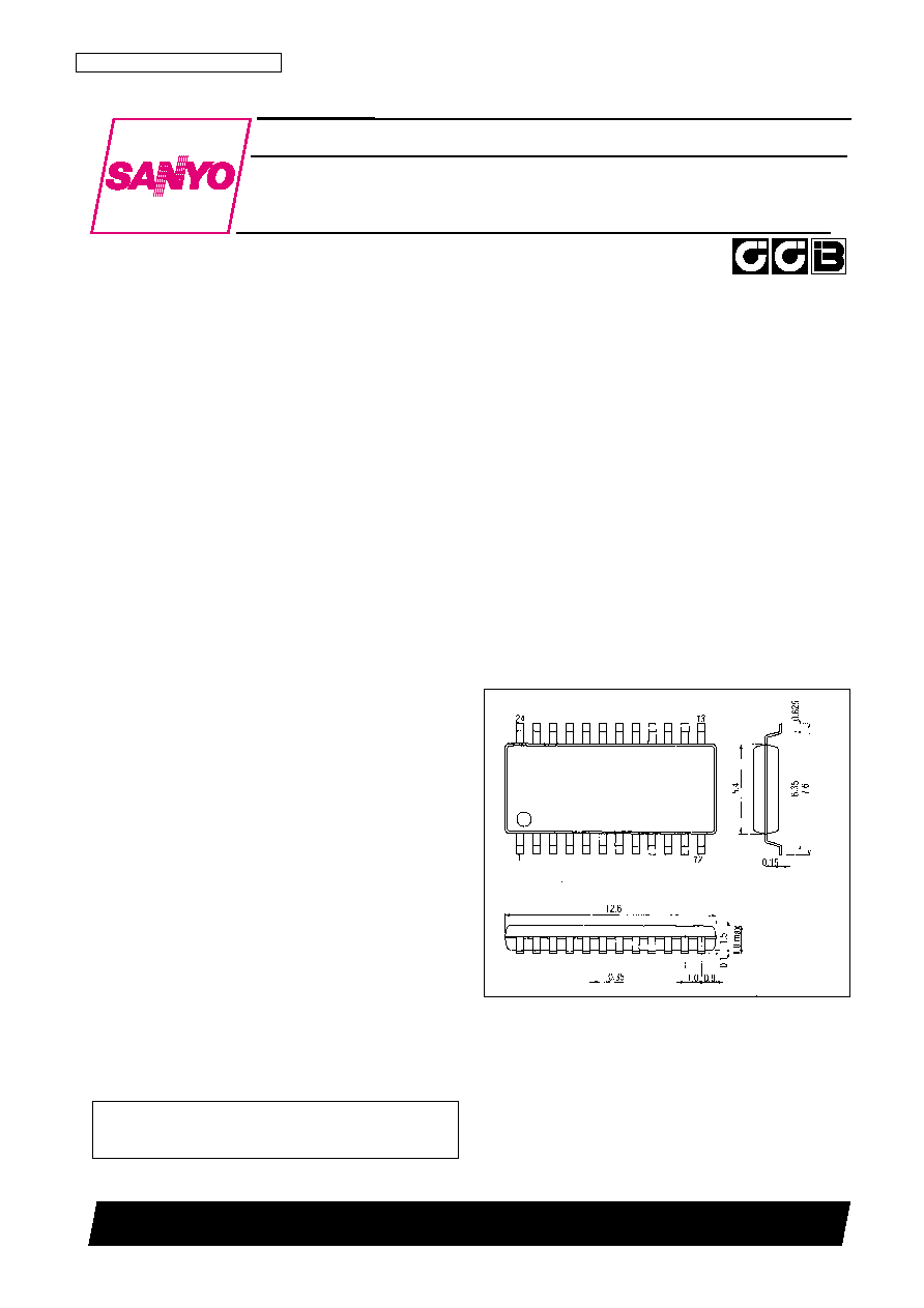
∑ Package: MFP24S
Package Dimensions
unit: mm
3112-MFP24S
CMOS IC
41098RM (OT) No. 5814-1/27
SANYO: MFP24S
[LC72134M]
SANYO Electric Co.,Ltd. Semiconductor Bussiness Headquarters
TOKYO OFFICE Tokyo Bldg., 1-10, 1 Chome, Ueno, Taito-ku, TOKYO, 110-8534 JAPAN
Dual PLL Frequency Synthesizer
for FM Tuner Systems
LC72134M
Ordering number : EN5814
∑ CCB is a trademark of SANYO ELECTRIC CO., LTD.
∑ CCB is SANYO's original bus format and all the bus
addresses are controlled by SANYO.
This product supports the Sanyo-original CCB bus format.
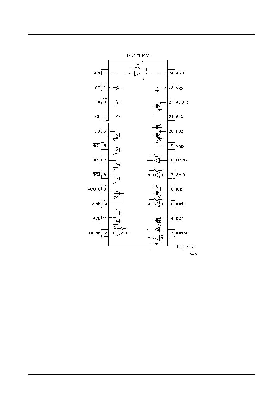
Pin Assignments
No. 5814-2/27
LC72134M
No. 5814-3/27
LC72134M
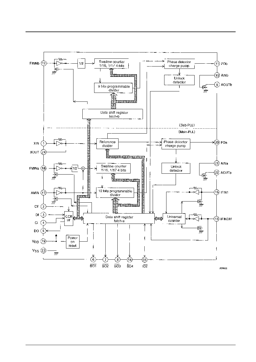
Block Diagram

No. 5814-4/27
LC72134M
Parameter
Symbol
Conditions
Ratings
Unit
Maximum supply voltage
V
DD
max
V
DD
≠0.3 to +7.0
V
V
IN
1 max
CE, DI, CL, AINa, AINb
≠0.3 to +7.0
V
Maximum input voltage
V
IN
2 max
XIN, FMINa, FMINb, AMIN, IFIN1, IFIN2/I1
≠0.3 to V
DD
+0.3
V
V
IN
3 max
IO2
≠0.3 to +15
V
V
O
1 max
DO
≠0.3 to +7.0
V
Maximum output voltage
V
O
2 max
XOUT, PDa, PDb
≠0.3 to V
DD
+0.3
V
V
O
3 max
BO1 to BO4, IO2, AOUTa, AOUTb
≠0.3 to +15
V
I
O
1 max
BO1
0 to +3.0
mA
Maximum output current
I
O
2 max
DO, AOUTa, AOUTb
0 to +6.0
mA
I
O
3 max
BO2 to BO4, IO2
0 to +10.0
mA
Allowable power dissipation
Pd max
Ta
85∞C
200
mW
Operating temperature
Topr
≠40 to +85
∞C
Storage temperature
Tstg
≠55 to +125
∞C
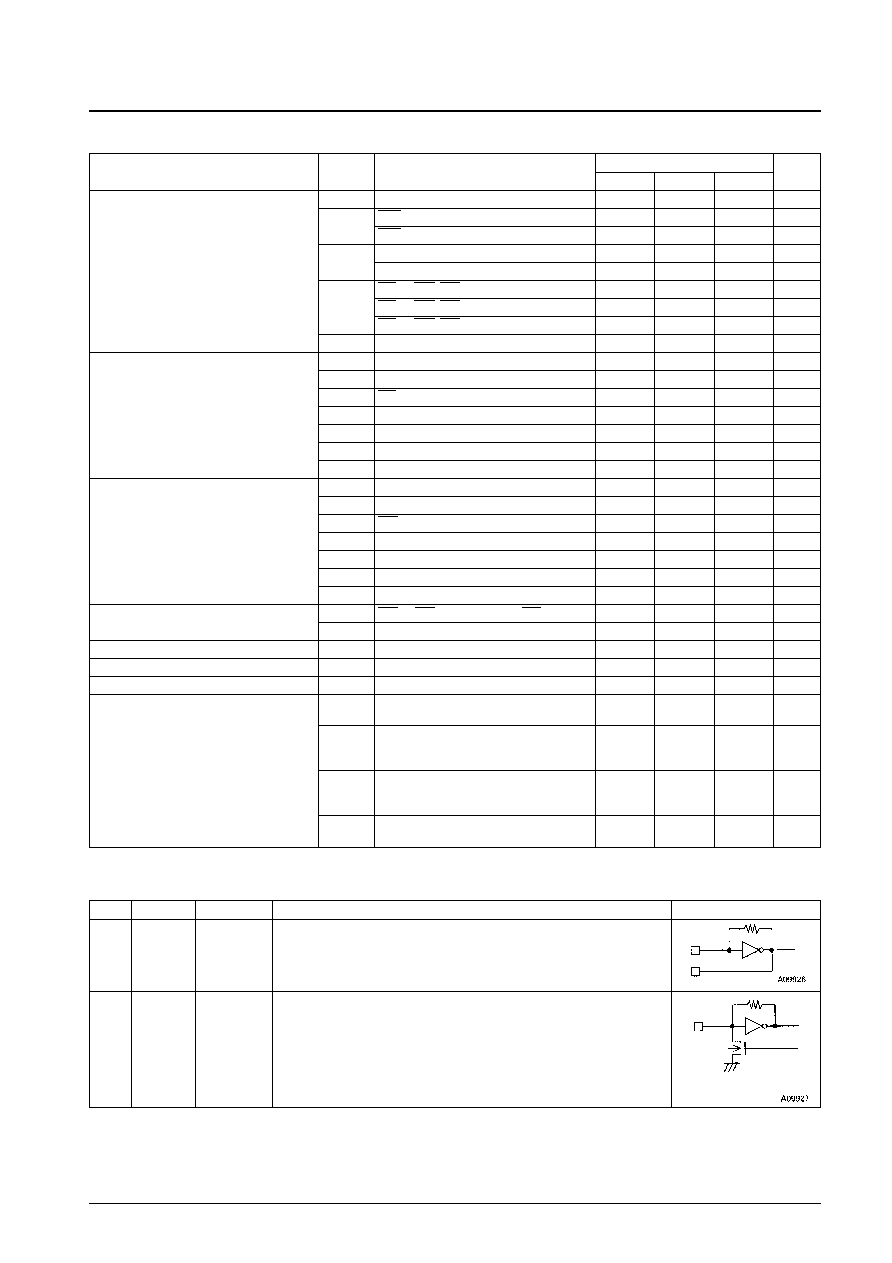
Specifications
Absolute Maximum Ratings
at Ta = 25∞C, V
SS
= 0 V
Parameter
Symbol
Conditions
Ratings
Unit
min
typ
max
Supply voltage
V
DD
V
DD
4.5
5.5
V
V
IH
1
CE, DI, CL
0.7 V
DD
6.5
V
Input high-level voltage
V
IH
2
IFIN2/I1
0.7 V
DD
V
DD
V
V
IH
3
IO2
0.7 V
DD
13
V
Input low-level voltage
V
IL
CE, DI, CL, IO2, IFIN2/I1
0
0.3 V
DD
V
Output voltage
V
O
1
DO
0
6.5
V
V
O
2
BO1 to BO4, IO2, AOUTa, AOUTb
0
13
V
f
IN
1
XIN: V
IN
1
1
8
MHz
f
IN
2
FMINa, FMINb: V
IN
2
10
160
MHz
Input frequency
f
IN
3
AMIN: V
IN
3, SNS = 1
2
40
MHz
f
IN
4
AMIN: V
IN
4, SNS = 0
0.5
10
MHz
f
IN
5
IFIN1, IFIN2/I1: V
IN
5
0.4
25
MHz
V
IN
1
XIN: f
IN
1
400
1500
mVrms
V
IN
2-1
FMINa, FMINb: f = 10 to 130 MHz
40
1500
mVrms
V
IN
2-2
FMINa, FMINb: f = 130 to 160 MHz
70
1500
mVrms
Input amplitude
V
IN
3
AMIN: f
IN
3, SNS = 1
40
1500
mVrms
V
IN
4
AMIN: f
IN
4, SNS = 0
40
1500
mVrms
V
IN
5
IFIN1, IFIN2/I1: f = 0.4 to 25 MHz, IFS = 1
70
1500
mVrms
V
IN
6
IFIN1, IFIN2/I1: f = 0.4 to 12 MHz, IFS = 0
100
1500
mVrms
Guaranteed crystal oscillator frequency
Xtal
XIN, XOUT:
*
1
4.0
8.0
MHz
Allowable Operating Ranges
at Ta = ≠40 to 85∞C, V
SS
= 0 V
Note: Recommended value for CI for the crystal oscillator element: CI
120
(4.5 MHz) or CI
70
(7.2 MHz)
However, since the oscillator circuit characteristics depend on the printed circuit board, circuit constants, and other factors, consult with the
manufacturer of the crystal element.
Parameter
Symbol
Conditions
Ratings
Unit
min
typ
max
Rf1
XIN
1.0
M
Internal feedback resistance
Rf2
FMINa, FMINb
500
k
Rf3
AMIN
500
k
Rf4
IFIN1, IFIN2/I1
250
k
Internal pull-down resistance
Rpd1
FMINa, FMINb
200
k
Rpd2
AMIN
200
k
Hysteresis
V
HIS
CE, DI, CL, IO2, IFIN2/II
0.1 V
DD
V
Output high-level voltage
V
OH
1
PDa, PDb: I
O
= ≠1 mA
V
DD
≠ 1.0
V
Electrical Characteristics
in the Allowable Operating Ranges
Continued on next page.
No. 5814-5/27
LC72134M
Parameter
Symbol
Conditions
Ratings
Unit
min
typ
max
V
OL
1
PDa, PDb: I
O
= 1 mA
1.0
V
V
OL
2
BO1: I
O
= 0.5 mA
0.5
V
BO1: I
O
= 1 mA
1.0
V
V
OL
3
DO: I
O
= 1 mA
0.2
V
Output low-level voltage
DO: I
O
= 5 mA
1.0
V
BO2 to BO4, IO2: I
O
= 1 mA
0.2
V
V
OL
4
BO2 to BO4, IO2: I
O
= 5 mA
1.0
V
BO2 to BO4, IO2: I
O
= 8 mA
1.6
V
V
OL
5
AOUTa, AOUTb: I
O
= 1 mA, AIN = 1.3 V
0.5
V
I
IH
1
CE, DI, CL: V
I
= 6.5 V
5.0
µA
I
IH
2
IFIN2/I1: V
I
= V
DD
, L/I1 = 0
5.0
µA
I
IH
3
IO2: V
I
= 13 V
5.0
µA
Input high-level current
I
IH
4
XIN: V
I
= V
DD
2.0
11
µA
I
IH
5
FMINa, FMINb, AMIN: V
I
= V
DD
4.0
22
µA
I
IH
6
IFIN1, IFIN2/I1: V
I
= V
DD
8.0
44
µA
I
IH
7
AINa, AINb: V
I
= 6.5 V
200
nA
I
IL
1
CE, DI, CL: V
I
= 0 V
5.0
µA
I
IL
2
IFIN2/I1: V
I
= 0 V, L/I1 = 0
5.0
µA
I
IL
3
IO2: V
I
= 0 V
5.0
µA
Input low-level current
I
IL
4
XIN: V
I
= 0 V
2.0
11
µA
I
IL
5
FMINa, FMINb, AMIN: V
I
= 0 V
4.0
22
µA
I
IL
6
IFIN1, IFIN2/I1: V
I
= 0 V
8.0
44
µA
I
IL
7
AINa, AINb: V
I
= 0 V
200
nA
Output off leakage current
I
OFF
1
BO1 to BO4, AOUTa, AOUTb, IO2: V
O
= 13 V
5.0
µA
I
OFF
2
DO: V
O
= 6.5 V
5.0
µA
High-level 3-state off leakage current
I
OFFH
PDa, PDb: V
O
= V
DD
0.01
200
nA
Low-level 3-state off leakage current
I
OFFL
PDa, PDb: V
O
= 0 V
0.01
200
nA
Input capacitance
C
IN
FMINa, FMINb
6
pF
I
DD
1
V
DD
: Crystal = 7.2 MHz, f
IN
2 = 130 MHz
5
10
mA
(FMINa operating), V
IN
2 = 40 mV rms
V
DD
: Crystal = 7.2 MHz, f
IN
2 = 130 MHz
I
DD
2
(FMINa and FMINb operating),
8
16
mA
Current drain
V
IN
2 = 40 mV rms
V
DD
: PLL block stopped (PLL INHIBIT mode)
I
DD
3
Crystal oscillator operating
0.5
mA
(crystal frequency: 7.2 MHz)
I
DD
4
V
DD
: PLL block stopped, crystal oscillator
10
µA
stopped
Continued from preceding page.
Pin Descriptions
Pin
Pin No.
Type
Function
Equivalent circuit
Xtal
∑ Crystal oscillator element connections (4.5 or 7.2 MHz)
XIN
XOUT
1
24
Main PLL
local oscillator
signal input
∑ FMINa is selected when DVS in the serial data is set to 1.
∑ Input frequency: 10 to 160 MHz
∑ The signal is passed through an internal divide-by-two prescaler and then input to
the swallow counter.
∑ The divisor can be set to a value in the range 272 to 65535. Since the internal
divide-by-two prescaler is used, the actual divisor will be twice the set value.
FMINa
18
Continued on next page.